A PCB layout maker is your gateway to turning circuit concepts into real, working boards. Every great electronic device starts with a well-planned PCB layout. It’s the foundation that determines performance, reliability, and manufacturability. This article walks you through selecting the right tools, avoiding common design pitfalls, and partnering with a manufacturer who ensures your design not only works but excels.
Are you facing these common struggles?
- Software Overwhelm: Too many PCB layout maker options, from free to professional, leaving you unsure which fits your project.
- Design-to-Production Gaps: Your file looks perfect on-screen but hits snags during manufacturing due to unclear specs or unsupported features.
- Costly Revisions: Small errors in layout lead to multiple prototype rounds, eating into time and budget.
- Tool Limitations: Free PCB layout maker software often lacks advanced features needed for complex or high-density designs.
- Supplier Miscommunication: Manufacturers struggle to interpret your design intent, resulting in delays or compromised quality.
At Best Technology, we bridge the gap between design and delivery. Here’s how we tackle these issues head-on:
- Tool-Agnostic Support: Whether you use KiCad, Altium, or an online PCB layout maker, we accept all major file formats and optimize them for production.
- DFM Integration: Our engineers pre-check your design for manufacturability, catching errors before they become costly.
- Rapid Prototyping: Streamlined processes turn your layout into a tangible PCB in days, not weeks.
- Advanced Capacity Support: From HDI to ceramic boards, we handle designs that free software can’t prepare for.
- Collaborative Engineering: We work with you to refine layouts for signal integrity, thermal management, and yield.
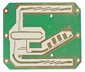
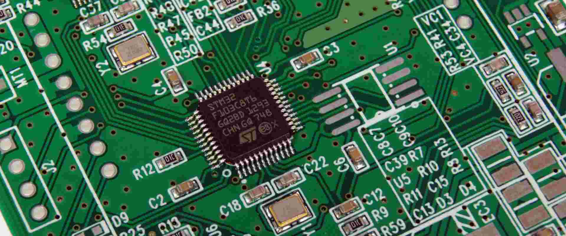
Think of a PCB layout as the blueprint of a building. It dictates where components sit, how they connect, and how signals flow. A clean layout means better performance; a messy one invites noise, heat, and failure. As a specialized PCB and assembly provider, Best Technology offers end-to-end support—from initial design review to box-build assembly. Do you have a project that need us to support? Just feel free to reach our team at sales@bestpcbs.com.
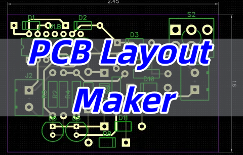
What Is a PCB Layout Maker?
A PCB layout maker is any software—free, online, or professional—that lets you arrange components and route traces on a virtual board. Popular examples include:
- KiCad: Open-source and powerful.
- EasyEDA: Browser-based for quick edits.
- Altium Designer: Industry favorite for complex projects.
These tools output Gerber or ODB++ files, which manufacturers use to produce physical boards. But a file alone isn’t enough. At Best Technology, we review your design for real-world constraints—like material choice and drill alignment—so your creation is not just viable but optimal.
Common Free and Professional PCB Layout Makers
Choosing the right PCB layout maker depends on your project’s needs. Here’s a quick comparison:
- KiCad – Best free PCB design software for enthusiasts and pros alike. No cost, no hidden limits.
- EasyEDA – Perfect for beginners. Its online PCB layout maker interface simplifies learning.
- Altium Designer – Top-tier for high-speed or multi-layer boards. Steep learning curve but unmatched depth.
- Fusion 360 – Integrates PCB layout with 3D modeling, great for mechanical fits.
We’ve seen files from all these platforms. Our job is to ensure your design—whether from a free PCB layout maker or a premium tool—translates flawlessly into production.
How to Select the Right PCB Layout Maker for Your Project?
Choosing a PCB layout maker can feel like standing in front of an open toolbox. They all look useful, but grabbing the wrong one can make your job much harder. The key isn’t to find the “best” tool overall, but the best one for you.
A great way to start is by asking three fundamental questions that will immediately narrow down your options.
1. What is the technical complexity of my board?
This is the most important factor. The needs of a hobbyist and a professional engineer are worlds apart.
- Simple & Low-Cost Projects: Are you creating a basic Arduino shield, a personal project, or a single-layer board for a simple circuit? For these, a free PCB layout maker like KiCad or an online tool like EasyEDA is a perfect starting point. They are more than capable of handling these tasks without the overhead of complex features.
- Medium Complexity & Professional Work: Is your design a 4 to 8-layer board with moderate component density, like a custom IoT device or an industrial controller? This is where tools like Fusion 360 (which includes ECAD and MCAD) or subscription-based versions of professional software shine. They offer advanced routing options and better library management.
- High Complexity & Advanced Applications: Are you designing a high-speed 16-layer motherboard, an RF communication module, or a board with HDI (High-Density Interconnect) technology? For these, industry-standard tools like Altium Designer or Cadence Allegro are necessary. Their powerful simulation engines for signal and power integrity are non-negotiable for getting the design right the first time.
2. What is my realistic budget, both now and later?
Be honest about what you can spend, not just on the software license, but on the entire project.
- Zero Budget (Free & Open Source): KiCad is the standout champion here. It’s completely free, with no restrictions on board size or layers. It’s a powerful statement that you can do professional work without a professional price tag.
- Low-Cost / Subscription Models: EasyEDA (free with premium features) and Fusion 360 (with a free startup/hobbyist license) offer a great balance. They lower the barrier to entry while providing a path to more advanced features.
- High Investment (Professional Licenses): Software like Altium Designer represents a significant investment (often thousands of dollars per year). However, for a company where design time is money, the efficiency, reliability, and advanced features can pay for themselves quickly by preventing costly respins.
3. How does my team need to collaborate?
Are you working alone, with a remote team, or with mechanical engineers in the next office?
- Individual Use: If you’re a solo inventor, any standalone software like KiCad or Altium will work. Your main concern is file compatibility with your manufacturer.
- Team-Based & Cloud-Collaborative: For teams spread across different locations, cloud-based PCB layout maker online platforms are a game-changer. EasyEDA and Altium 365 allow multiple people to work on the same design simultaneously, with version control and real-time commenting, eliminating the nightmare of managing different file versions.
You’ve chosen your tool and perfected your layout. But here’s a pro tip: the final, and perhaps most crucial, step happens before you even generate your Gerber files. Talk to your manufacturer as soon as you have a draft.
Why? Because we see designs every day that look perfect on screen but contain hidden manufacturing challenges. At Best Technology, we offer a free Design for Manufacturability (DFM) check at the early design stage.
When you involve us early, our engineers can provide proactive feedback on:
- Trace Widths and Clearances: Are they suitable for our advanced etching process, ensuring reliability?
- Drill Sizes and Pad Sizes: Are your holes drillable without causing reliability issues, especially in vias?
- Layer Stack-up: Is the material and thickness order optimal for signal integrity and cost-effectiveness?
- Solder Mask and Silkscreen: Is the text legible? Are there any mask slivers that could cause short circuits?
This collaborative approach transforms the PCB layout maker from a solitary design tool into the first step of a seamless production pipeline. By letting us provide input on your PCB layout design, we can often catch minor issues that would otherwise lead to a failed prototype, saving you time, money, and frustration. It’s the smartest way to ensure your digital creation becomes a flawless physical product.
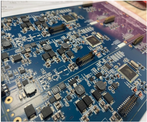
Turning Your PCB Layout into a Real Product
This is where vision meets reality. The journey has clear steps:
- File Submission: Send us your Gerbers, ODB++, or native design files.
- Engineering Review: We analyze DFM (Design for Manufacturability) and suggest refinements.
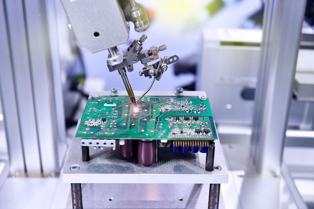
- Fabrication: Using laser drills and automated optical inspection, we build your board layer by layer.
- Assembly: Components are placed, soldered, and tested.
- Testing & Shipping: Every board undergoes electrical and functional checks.
Our capabilities include HDI, ceramic substrates, and lead-free finishes. With Best Technology, your design transitions into a product backed by predictable performance and yield.
How to Make a Printed Circuit Board?
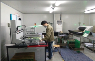
BEST Technology is a professional PCB manufacturer with extensive experience in producing high-quality printed circuit boards. We utilize advanced equipment and strict quality control processes to ensure every PCB meets our clients’ specifications.
1. Material Selection and Preparation
We begin with carefully selected materials based on your specific requirements:
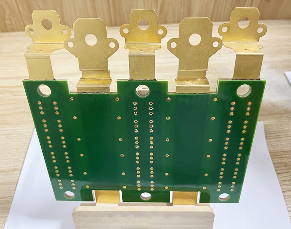
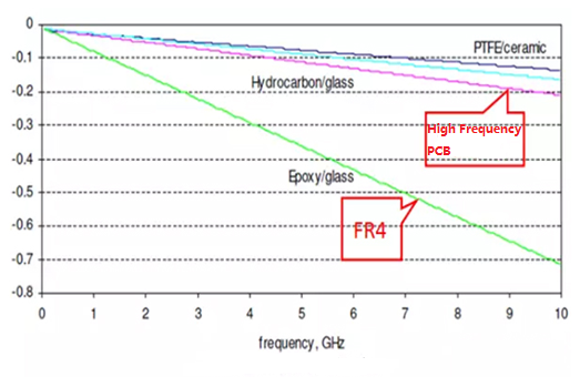
- Base Materials: FR-4 (various TG values), high-frequency materials (Rogers, Taconic), metal core substrates
- Copper Foil: Range from 1/2OZ to 30OZ thickness options
- Prepreg: Various types (1080, 2116, 7628) for interlayer bonding
2. Inner Layer Processing
- Board Cutting: Precisely cut large panels to required working dimensions
- Inner Layer Circuitry: Dry film application, exposure, development, and etching
- AOI Inspection: Automated optical inspection to ensure circuit quality
- Brown Oxidation: Surface treatment to enhance bonding capability
3. Multi-layer Lamination
- Layer Stack-up: Precise alignment of inner layers with prepreg
- Hot Pressing: High temperature (around 200°C) and pressure application
- Cooling Process: Controlled cooling to prevent warping and twisting
4. Drilling Process
- Mechanical Drilling: Capable of drilling holes from 0.15mm to 6.5mm diameter
- Laser Drilling: For micro-vias as small as 0.07mm
- Aspect Ratio: Up to 25:1 for through-holes
- Special Capabilities: Back drilling, controlled depth drilling, and slot machining
5. Plating and Metallization
- Electroless Copper Deposition: Creates conductive layer in hole walls (1-3μm)
- Panel Plating: Builds up copper thickness using advanced chemistry
- Pattern Plating: Selective copper and tin plating for circuit formation
6. Outer Layer Circuit Formation
- Dry Film Application: High-precision pattern transfer
- Exposure and Development: Using LDI technology capable of 2.5/2.5mil line width/spacing
- Etching: Precise copper removal to create circuit patterns
7. Solder Mask Application
- Ink Types: Various colors available (green, black, blue, red, white, yellow, purple)
- Application Methods: Both screen printing and coating processes
- Precision: Minimum solder mask bridge of 3-4mil depending on copper thickness
8. Surface Finishing
We offer comprehensive surface treatment options:
- Lead-free HASL: For general applications
- ENIG: Excellent for fine-pitch components
- Immersion Silver/Tin: Cost-effective alternatives
- Gold Finger Plating: For edge connectors
- ENEPIG: Advanced surface finish for demanding applications
9. Final Processing
- Legend Printing: Screen printing or inkjet printing of component markings
- Profile Routing: CNC machining for precise board outlines
- V-scoring: For panel separation with various angle options
- Electrical Testing: Flying probe or test fixture methods
BEST Technology’s Manufacturing Capabilities
Material Expertise
- Standard FR-4: TG130-TG180 options
- High-Frequency Materials: Rogers, Taconic, Arlon series
- High-Speed Materials: Various loss grades for different frequency requirements
- Metal Core PCBs: Aluminum and copper substrates for thermal management
Technical Specifications
- Layer Count: 1-50 layers standard, up to 100 layers with review
- Board Thickness: 0.4mm to 6mm standard, 0.15mm to 10mm extended range
- Copper Thickness: 0.5OZ to 28OZ (outer), 0.5OZ to 20OZ (inner)
- Minimum Line Width/Spacing: 3/3mil for standard applications
Quality Assurance
- IPC Standards: Compliance with IPC Class 2 and Class 3 requirements
- Testing Capabilities: Advanced equipment for comprehensive quality verification
- Process Control: Strict monitoring at every manufacturing step
Competitive Advantages
Technical Excellence
- Advanced Equipment: State-of-the-art manufacturing and inspection tools
- Engineering Expertise: Experienced team capable of handling complex designs
- Quality Focus: Commitment to delivering reliable, high-performance PCBs
Comprehensive Service
- Design Support: Assistance with stack-up design and DFM optimization
- Material Guidance: Expert recommendations based on application requirements
- Rapid Prototyping: Quick turnaround for design verification
Quality Commitment
- Stringent Inspection: Multiple checkpoints throughout manufacturing
- Performance Verification: Electrical testing and impedance control
- Reliability Assurance: Materials and processes selected for long-term performance
At BEST Technology, we combine advanced manufacturing capabilities with rigorous quality control to deliver PCBs that meet the most demanding specifications. Our comprehensive approach ensures that every board we produce meets the highest standards of quality and reliability.
Best Practices and PCB Layout Tips from PCB Experts at BEST Technology
After finalizing your schematic, the PCB layout stage is where theoretical design transforms into a physically viable product. A well-executed layout is paramount to the functionality, reliability, and manufacturability of your board. At BEST Technology, our engineers have identified key areas where strategic layout decisions prevent common pitfalls and significantly enhance performance.
1. Mastering Component Placement
Think of component placement as arranging the rooms in a house for optimal flow. Proper placement sets the stage for efficient routing and optimal performance.
- Group by Function: Place related components (e.g., a microcontroller and its decoupling capacitors and crystal) close together. This minimizes trace lengths and reduces noise.
- Consider Signal Flow: Arrange components to facilitate a logical, direct signal path from input to output, avoiding unnecessary backtracking or crossing of sensitive signals.
- Plan for Heat Dissipation: Identify high-power components early and position them to allow for adequate cooling. Avoid clustering heat-generating parts.
- Keep Connectors Accessible: Place connectors, especially those for user interfaces or external cables, along the board edges for easy access.
2. Power Distribution Network (PDN) Design
A robust PDN is the backbone of your board, preventing erratic behavior and ensuring all components receive clean, stable power.
- Use Power Planes Where Possible: Solid power planes offer low-impedance power distribution, which is superior to routing power with traces.
- Implement a Strategic Decoupling Scheme: Place small-value decoupling capacitors (e.g., 100nF) as close as possible to the power pins of each IC. Use larger bulk capacitors (e.g., 10uF) near the board’s power entry point to handle slower current demands.
- Mind Your Return Paths: Current must have a clear, low-impedance path back to its source. Avoid splitting ground planes underneath high-speed signal traces, as this can create large loop areas and act as an antenna.
3. Signal Integrity Fundamentals
How you route your traces directly impacts signal quality, especially in high-speed designs.
- Control Impedance: For high-speed signals (like USB, HDMI, DDR), the trace must have a consistent characteristic impedance (e.g., 50Ω single-ended, 100Ω differential). This is controlled by trace width, copper thickness, and the distance to the reference plane. Our team can provide you with the correct stack-up and trace width calculations.
- Route Differential Pairs Correctly: The two traces in a differential pair must be of equal length and closely spaced to maintain noise immunity. Route them together from start to finish.
- Minimize Via Use in High-Speed Paths: Each via introduces a small discontinuity in impedance. For critical signals, minimize the number of vias used.
4. The Critical Role of Grounding
A poor grounding strategy is a common source of noise and interference.
- Use a Continuous Ground Plane: A solid ground plane on an adjacent layer provides a stable reference for signals and a low-impedance return path.
- Separate Analog and Digital Grounds: If your board has both analog and digital sections, partition the ground plane to prevent noisy digital return currents from corrupting sensitive analog signals. Connect these grounds at a single point, typically under the ADC or at the power supply.
5. Design for Manufacturing (DFM)
A perfect design in software is useless if it can’t be reliably manufactured. Adhering to DFM rules saves time and cost.
- Respect Clearance Rules: Maintain adequate spacing between traces, pads, and copper pours. Our standard capability is 3/3mil (line/space), but designing with larger clearances where possible improves yield.
- Thermal Relief for Pads: Use thermal relief connections (spoked connections) for pads connected to large copper pours or power planes. This prevents heat from sinking away during soldering, which can lead to cold solder joints.
- Solder Mask and Silkscreen: Ensure solder mask dams between fine-pitch component pins are sufficient to prevent bridging. Keep silkscreen legible and away from solderable areas.
Even with the best practices, simulation is key to predicting real-world behavior. Before you commit to a prototype, our engineering team can provide an added layer of confidence through advanced analysis:
- Signal Integrity Simulation: We analyze your high-speed paths for reflections, crosstalk, and timing issues.
- Power Integrity Simulation: We verify that your PDN will deliver stable voltage to all components, even under peak current demands.
- Thermal Analysis: We can identify potential hot spots and suggest layout improvements for better heat dissipation.
By partnering with BEST Technology from the layout stage, you leverage years of manufacturing expertise. We help you create a design that not only works on paper but is also optimized for performance, reliability, and efficient production.
It is clear that a PCB layout maker gives you the power to create. But the right partner simplifies the path from prototype to production. From design to delivery, Best Technology ensures your ideas become robust, market-ready products.
We offer PCB layout design support, prototyping in as little as 24 hours, fabrication and full turnkey assembly. Pls feel free to send your files to sales@bestpcbs.com for a fast, free quote.
FAQs
Q1: What is the difference between IPC Class 2 and IPC Class 3 standards for PCBs?
- A: IPC Class 2 is designed for standard consumer electronics, where high reliability is not critical and a longer product life is expected. IPC Class 3 is for high-reliability or harsh-environment applications, such as industrial, automotive, aerospace, and medical equipment, where continuous performance and extended life are essential. The difference lies in stricter acceptance criteria for Class 3, requiring more precise manufacturing control over parameters like drilling accuracy, copper plating thickness in holes, and solder mask thickness.
Q2: Are you capable of manufacturing PCBs to the IPC Class 3 standard, and is the price difference significant?
- A: Yes, we are fully capable of producing PCBs that meet the stringent IPC Class 3 standard. The price premium for Class 3 is typically 10%-15% higher than for Class 2, reflecting the enhanced process controls, materials, and inspection required.
Q3: Can you assist with the stack-up design for our PCB?
- A: Absolutely. We can design the PCB stack-up according to your requirements. Please provide us with the necessary details, such as the number of layers, copper weight (oz), and the desired final board thickness.
Q4: What payment methods do you accept, and are credit terms (e.g., monthly credit) available?
- A: We accept payments via PayPal, T/T (Bank Wire Transfer), and Western Union. For new customers, we require 100% payment in advance. Upon establishing a stable cooperation history and reaching a certain order volume, we can discuss other payment arrangements, such as net monthly terms.