The 365nm 35*35 LED PCB is gaining significant traction in various industries, especially for applications requiring efficient UV light. From curing to disinfection, this compact and high-performance PCB is setting new standards. In this blog, we’ll explore what makes the 365nm 35*35 LED PCB so effective and how it’s different from traditional LED PCBs. We’ll also discuss its benefits, industries that rely on it, and how to integrate it into existing systems.
What Is PCB in LED?
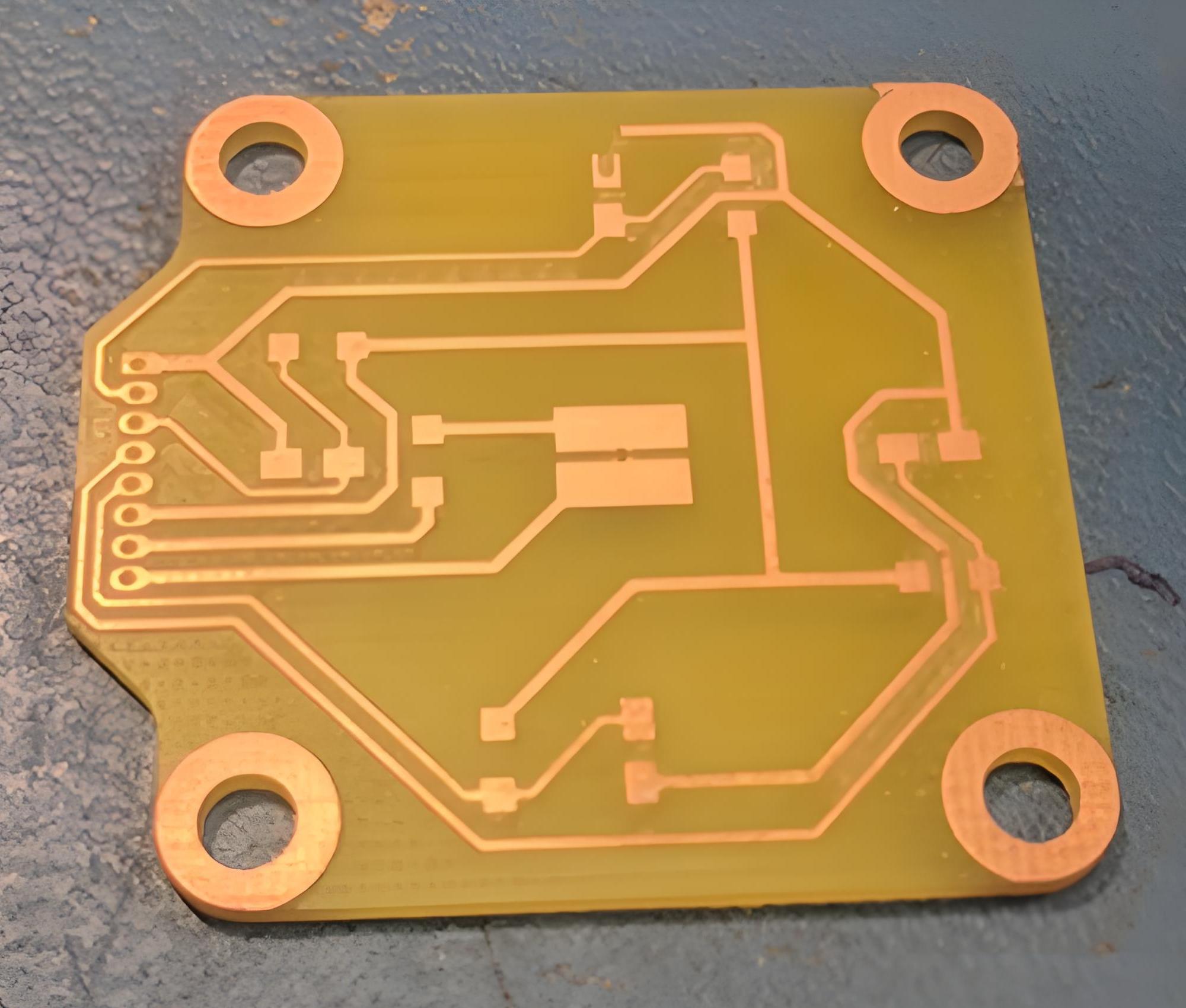
Before diving into the specifics of the 365nm 35*35 LED PCB, let’s first understand what PCB means in the context of LED technology. A PCB, or printed circuit board, serves as the foundation for electronic components. In LED applications, it provides the electrical connections that power the LED diodes. This allows the LED to perform efficiently while managing heat and ensuring a stable operation over time.
PCBs are vital in supporting various LED applications. They come in many shapes and sizes, designed to optimize the performance of LEDs in various systems. The 365nm 35*35 LED PCB is no exception, providing the ideal platform for a compact and efficient UV LED source.
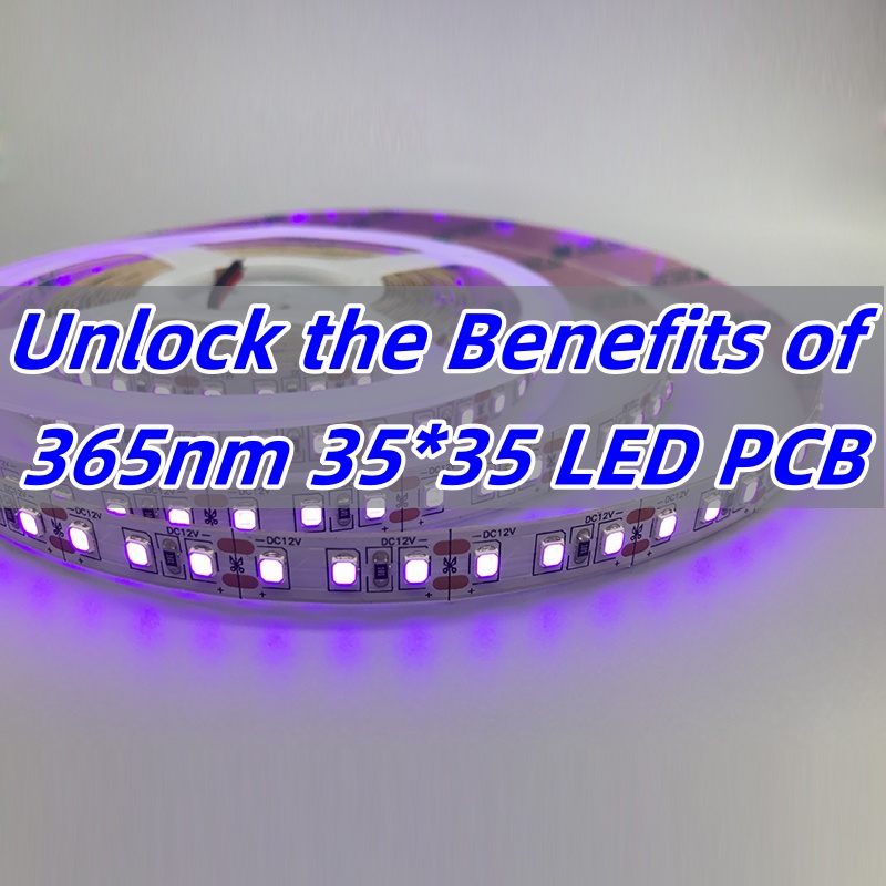
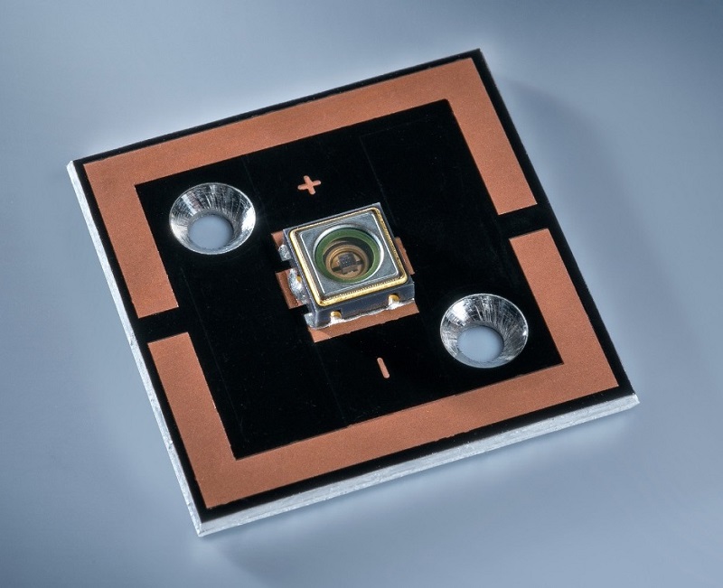
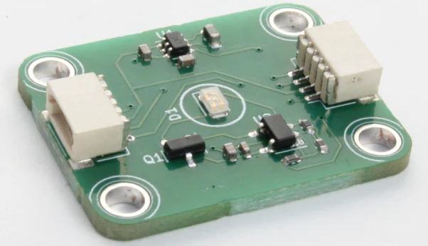
What Is a 365nm 35*35 LED PCB?
A 365nm 35*35 LED PCB features a UV LED with a wavelength of 365 nanometers, which is particularly effective for a range of UV-related applications. The “35*35” usually refers to the size of the LED lamp beads, with the unit being millimeters (mm). The 35*35 size refers to the compact nature of the PCB, providing a high-density array of LEDs on a small surface area. This compact design makes the PCB ideal for applications where space is limited but power and efficiency are still required.
The 365nm wavelength is commonly used for tasks like curing inks, coatings, and adhesives. It’s also crucial in sterilization, medical devices, and various types of sensors. This type of PCB offers precise, reliable UV light output, ensuring that the applications benefit from high energy efficiency and performance.
What Are the Differences Between 365nm 35*35 LED PCB and Traditional LED PCBs?
The 365nm 35*35 LED PCB differs significantly from traditional LED PCBs, mainly due to its specialized UV wavelength and compact design. Traditional LED PCBs often emit light in the visible spectrum, ranging from red to blue. However, the 365nm LED emits ultraviolet light, which is essential for specialized tasks like curing and disinfection.
Additionally, traditional LED PCBs are typically larger, whereas the 365nm 35*35 LED PCB is designed to fit into tight spaces. This makes it especially useful in compact devices or systems that require high-performance LED technology but don’t have room for larger PCBs. This size and the targeted UV wavelength make the 365nm 35*35 LED PCB a versatile solution for industries requiring precision and efficiency.
What Industries Use 365nm 35*35 LED PCBs?
The 365nm 35*35 LED PCB finds applications across many industries, particularly those that rely on UV light for specific functions. Some of the key industries include:
Medical Industry: For sterilization and disinfection of medical tools and surfaces.
Electronics Manufacturing: In the curing of adhesives used in the assembly of electronic devices.
Printing and Packaging: Used in curing inks and coatings quickly and efficiently.
Laboratory Research: For UV detection and analysis in various research settings.
These industries benefit from the 365nm wavelength, as it is highly effective in promoting chemical reactions, curing, and sterilization, among other tasks. The compact size of the PCB also allows for easy integration into existing systems, making it a popular choice for applications that need both precision and space-saving design.
How Does 365nm 35*35 LED PCB Benefit UV Curing?
One of the primary benefits of the 365nm 35*35 LED PCB is its ability to enhance UV curing processes. UV curing is a process that uses ultraviolet light to quickly dry or harden materials such as inks, paints, and coatings. The 365nm wavelength is particularly effective in activating photoinitiators in these materials, allowing for faster curing times and more durable results.
The compact design of the 35*35 PCB makes it ideal for use in curing systems, where space is often at a premium. This PCB provides uniform light distribution and consistent power, ensuring that materials are cured evenly and efficiently. Whether in large industrial curing systems or small desktop devices, the 365nm 35*35 LED PCB offers a reliable, energy-efficient solution.
How Does 365nm 35*35 LED PCB Improve Energy Efficiency?
Energy efficiency is a critical factor in modern LED technology, and the 365nm 35*35 LED PCB is designed with this in mind. Unlike traditional light sources, which waste a significant amount of energy in the form of heat, LED PCBs are much more efficient. The 365nm 35*35 LED PCB uses less power to generate high-intensity UV light, reducing overall energy consumption.
This efficiency translates into lower operating costs and a smaller environmental footprint. For industries relying on UV light, the 365nm 35*35 LED PCB offers a significant advantage by providing more light with less power, making it an excellent choice for businesses looking to reduce energy costs while maintaining high performance.
Why Use a 365nm 35*35 LED PCB for Disinfection?
The 365nm 35*35 LED PCB is an excellent choice for disinfection due to the effectiveness of UV light at this specific wavelength. UV-C light, which is typically in the range of 200-280 nm, is known for its ability to kill bacteria, viruses, and other pathogens. The 365nm wavelength falls just outside this range but is still highly effective in disinfecting surfaces and air.
In addition to its effectiveness, the compact size of the 365nm 35*35 LED PCB allows it to be integrated into a wide range of disinfection systems, from handheld devices to larger industrial units. It provides a powerful, efficient solution for sanitation in medical, commercial, and residential environments.
How to Integrate 365nm 35*35 LED PCBs into Existing Systems?
Integrating the 365nm 35*35 LED PCB into existing systems is straightforward, especially given its compact size and compatibility with standard UV systems. The PCB can be installed in existing UV curing or sterilization units with minimal modification. Its small form factor makes it ideal for retrofitting into systems where space is limited.
In addition to the physical integration, the 365nm 35*35 LED PCB is designed to be energy-efficient and long-lasting, which can help extend the lifespan of the system it’s added to. Whether you’re upgrading an existing system or designing a new one, this PCB provides a reliable and cost-effective way to enhance UV applications without the need for major changes.
The 365nm 35*35 LED PCB is a powerful and versatile solution for UV applications. Whether used in curing, disinfection, or other specialized tasks, it offers numerous advantages over traditional LED PCBs. Its compact design, energy efficiency, and effectiveness in UV light generation make it a must-have for industries looking to improve performance while saving space and energy.
With the ability to integrate seamlessly into existing systems, the 365nm 35*35 LED PCB is poised to revolutionize how businesses approach UV technology. By incorporating this advanced PCB into your systems, you can ensure greater efficiency, reliability, and sustainability. If you’re looking for a supplier who can provide high-quality 365nm 35*35 LED PCBs, Best Technology is your trusted partner. Just feel free to reach out to us to us at sales@bestpcbs.com.