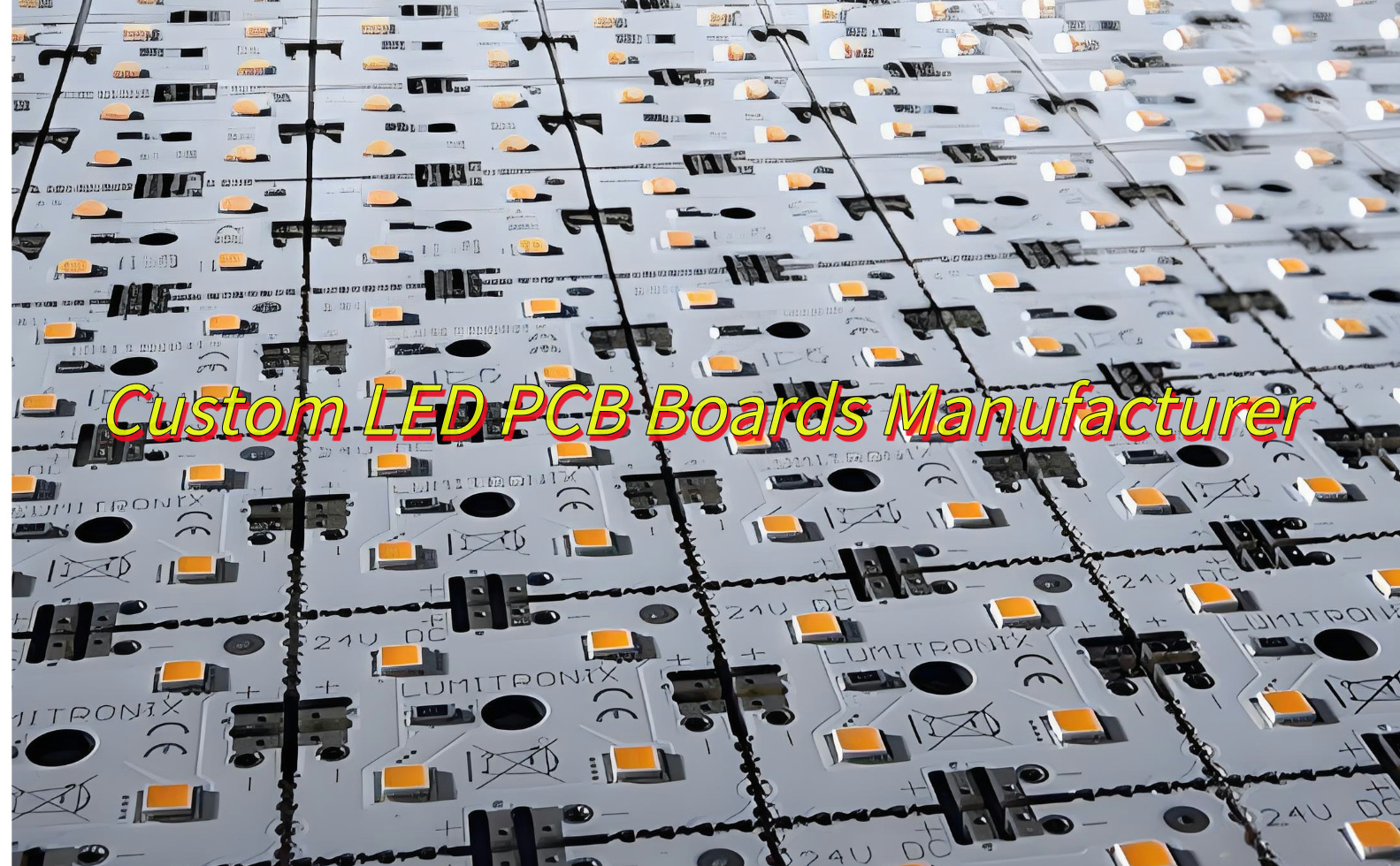
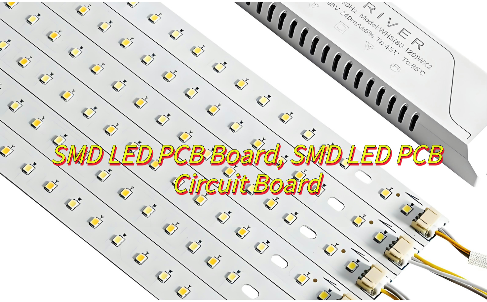
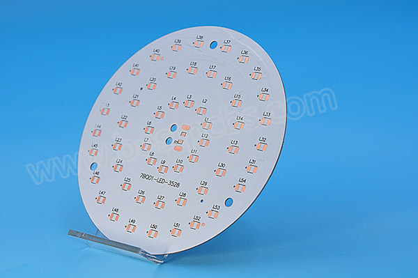
The Importance of Printed Circuit Boards
Nowadays, printed circuit boards (PCBs) are the backbone of modern electronics. They provide a structured way to connect electronic components, so that devices can function efficiently. Whether in household gadgets, medical equipment, industrial machines, or communication systems, PCBs are everywhere.
However, like any other electronic component, PCBs can develop faults over time. When a PCB fails, the entire device may stop working. Instead of replacing the whole unit, repairing the PCB can be a cost-effective solution. Not only does this save money, but it also reduces electronic waste, which is beneficial for the environment. At Best Technology, we not only fabricate PCB, but also offer circuit board repair service. Our repair guys have 10 years experiences in this industry, you just need to send back your failed PCB to us, then our guys can troubleshoot it very quickly.
Why Do Printed Circuit Boards Fail?
PCB can be failed due to several factors, component damage, short circuits, overheating and so on. Here we listing some common failures in our daily life:
1. Physical Damage
Dropping, bending, or mishandling a device can crack the PCB or damage solder joints. Even minor stress on the board can cause fractures in the copper traces, leading to connectivity issues.
2. Moisture and Contamination
PCBs and components on PCBs are sensitive to moisture. Exposure to humidity or water can lead to corrosion, which can destroy metal contacts and traces. Contaminants like dust, dirt, and chemical residues can also cause shorts and malfunctions.
3. Overheating and Poor Heat Dissipation
Electronic components generate heat during operation. If a PCB lacks proper heat management, components can overheat, causing them to degrade or fail. Poor ventilation, blocked cooling fans, or excessive current loads can worsen this issue.
4. Electrical Overload and Power Surges
Power fluctuations can damage a PCB. Sudden voltage spikes from lightning, faulty power supplies, or unstable electrical systems can cause components to burn out. Using surge protectors and voltage regulators helps prevent these problems.
5. Manufacturing Defects
Some PCB failures originate from the manufacturing process. Defective soldering, poor-quality components, or design flaws can lead to malfunctions. So, choosing a reliable PCB and PCBA manufacturer is necessary to ensure the high performance of PCB.
Can Circuit Boards Be Repaired?
Yes, many PCB failures can be fixed with the right expertise and tools. A damaged PCB doesn’t always mean the entire device is beyond repair. Skilled technicians can diagnose issues, replace faulty components, and restore connections to bring the board back to life. But not all failures can be repaired, only in such conditions:
- If the damage is limited to a few burnt or broken components.
- If the circuit traces are slightly damaged but can be restored.
- If the failure is due to poor soldering or loose connections.
So, when is replacement necessary?
- If the PCB has multiple layers with extensive damage.
- If the cost of repair exceeds the cost of a new board.
- If proprietary components are damaged beyond replacement.
For most cases, a professional circuit board repair service can determine whether fixing the board is practical.
How Much Does It Cost to Repair a Circuit Board?
The cost of repairing a circuit board depends on several factors, including the complexity of the board, the extent of damage, the type of components involved, and whether the repair is done professionally or as a DIY project. Below, we’ll break down the cost considerations in detail.
1. Factors Affecting Circuit Board Repair Costs
a) Type and Complexity of the Circuit Board
- Simple single-layer PCBs (used in basic electronics) are easier and cheaper to repair.
- Multilayer PCBs (found in advanced devices like medical equipment, industrial machines, and automotive electronics) require specialized tools and expertise, increasing costs.
b) Type of Damage
- Minor issues (e.g., loose connections, broken traces, or burnt resistors) are inexpensive to fix.
- Major failures (e.g., damaged ICs, burned PCB layers, or extensive corrosion) require expensive replacements or rework.
c) Labor and Service Costs
- Professional repair services charge based on time, complexity, and technician expertise.
- DIY repairs save on labor costs but require proper tools and skills.
d) Tools and Equipment
- Basic tools like a soldering iron, multimeter, and flux are affordable.
- Advanced tools like an oscilloscope, reflow station, or thermal imaging camera increase costs.
e) Component Replacement Costs
- Common components (resistors, capacitors, and diodes) cost a few cents to a few dollars.
- Specialized components (microcontrollers, power modules, or custom ICs) can cost $50 or more.
2. Estimated Cost Breakdown for PCB Repair
| Repair Type | Professional Repair Cost ($) | If PCB Made in Best Technology |
| Solder joint rework | 20 – 50 | Free |
| Broken trace repair | 30 – 100 | Free |
| Resistor/capacitor replacement | 20 – 50 | Free |
| IC/microcontroller replacement | 50 – 300 | Free |
| Severe burn damage repair | 200 – 600 | Free |
| Full PCB rework | 300 – 1000+ | Free |
Circuit Board Repair Tools
If you want to do circuit board repair by yourself, then prepare these tools first:
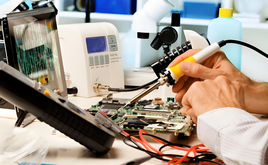
1. Soldering Iron and Solder
You will use them when reattaching loose connections and replacing components. During the repairing, a temperature-controlled soldering iron can make sure precision without overheating components.
2. Solder Wick
Removing excess solder is necessary when replacing components. A desoldering pump and wick help clean connections properly.
3. Multimeter
This is used to test PCB function after repairing. It can be used to measure voltage, resistance, capacitance and trace continuity (make sure no circuit short or open circuit), helping to identify broken traces or faulty components.
4. Magnification Tools
Some tiny failures can’t be checked by our naked eyes, so a magnifying glass is necessary to inspect small solder joints and identify small cracks or defects on a PCB.
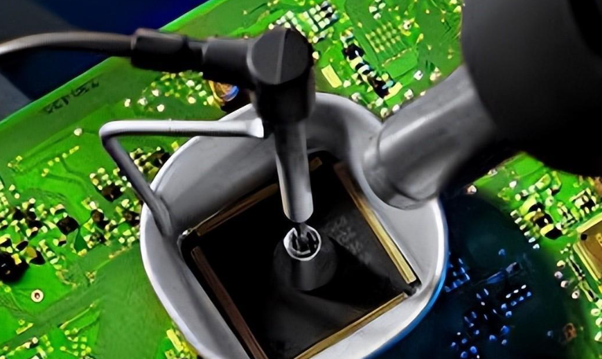
How to Repair a Circuit Board?
Repairing a circuit board requires a systematic approach to diagnose and fix faults. Whether you’re dealing with broken traces, damaged components, or burnt areas, the right tools and techniques ensure a successful repair. Let’s try to repair a failed PCB step by step:
1. Gather circuit board repair tools
Prepare the tools that I mentioned as above. Of course, it is better if you have some other tools like tweezers and a heat gun. A tweezer can help to move the small components and heat gun is used to rework SMD components.
2. Identify the problem (troubleshooting)
Located the issue through visual inspection, where you check for broken traces, burnt areas, or loose components. A continuity test with a multimeter helps identify broken circuits, while component testing ensures resistors, capacitors, and ICs are functioning correctly. If the board is not physically damaged, power it on at safe condition and measure voltage at key points. Here are some 4 common failures and troubleshooting steps:
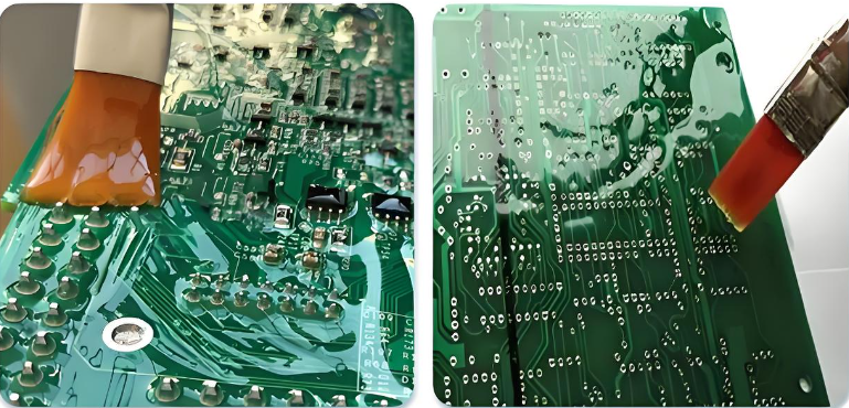
a) For repairing broken traces, clean the damaged area and scrape off the solder mask around the break firstly. Then use a solder bridge, jumper wire, or copper wire to reconnect the circuit. After soldering, apply a protective solder mask to prevent further damage.
b) When dealing with loose or cold solder joints, reheat the existing solder with a soldering iron and apply fresh solder for a stronger bond. Flux can help achieve a smooth and reliable connection. Inspecting with a magnifying glass ensures there are no solder bridges or weak connections.
c) If a damaged component is found, carefully desolder it using a pump or wick to remove excess solder. Once removed, insert the new component, make sure solder it with correct polarity and alignment. Solder it in place, trim any excess leads, and check for proper connection with a multimeter.
d) For burnt PCB repairs, cut out the charred section if necessary, then reconstruct missing traces using copper tape or jumper wires. Applying epoxy or solder mask reinforces the repair, preventing further deterioration.
3. Testing after repairing
After completing repairs, conduct a final test by visually inspecting the board, checking continuity with a multimeter, and powering it on under normal conditions. Monitor voltage levels and ensure the repaired components function correctly. If the board operates as expected, the repair is successful.
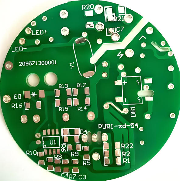
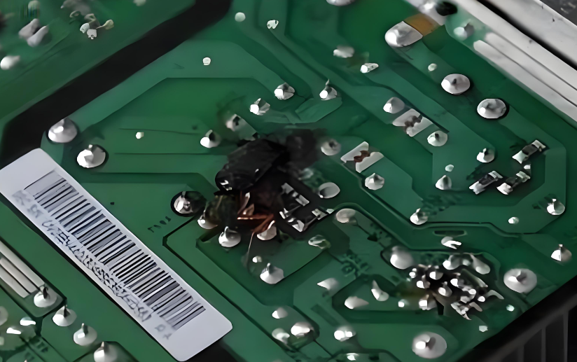
How to Tell If a Circuit Board Is Fried?
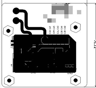
It is very easy to check whether my PCB is fried. We can see it by our eyes, because the fried PCB always have a black color in the burnt area. Other abnormal situation also shows your PCB is fried, like traces cracked or broken means short circuit, and the swollen or leaking capacitors is a sign of electrical failure. Carefully check your PCBs if it is out of work suddenly. Here are some functional signs that means your PCB is fired:
- Device doesn’t power on – Could be a blown fuse or damaged trace.
- Intermittent operation – Loose connections or weak solder joints.
- Unusual smell – A burnt smell suggests overheating damage.
Where Can I Get a Circuit Board Repaired?
If you’re searching for circuit board repair near me, working with Best Technology is the best option. We are a 18 years experienced PCB & PCBA manufacturer, we offer one-stop service from PCB layout, schematics, PCB manufacturing, components souring, PCB assembly, box building assembly, IC programming, and circuit board repairing.
We have professional repair guys that specialized to repair and rework PCBAs. We provide fast turnaround service, it means we can minimize downtime with quick repairs and save much money compared to full replacements. If you need repair circuit boards services, Best Technology is your trusted partner.