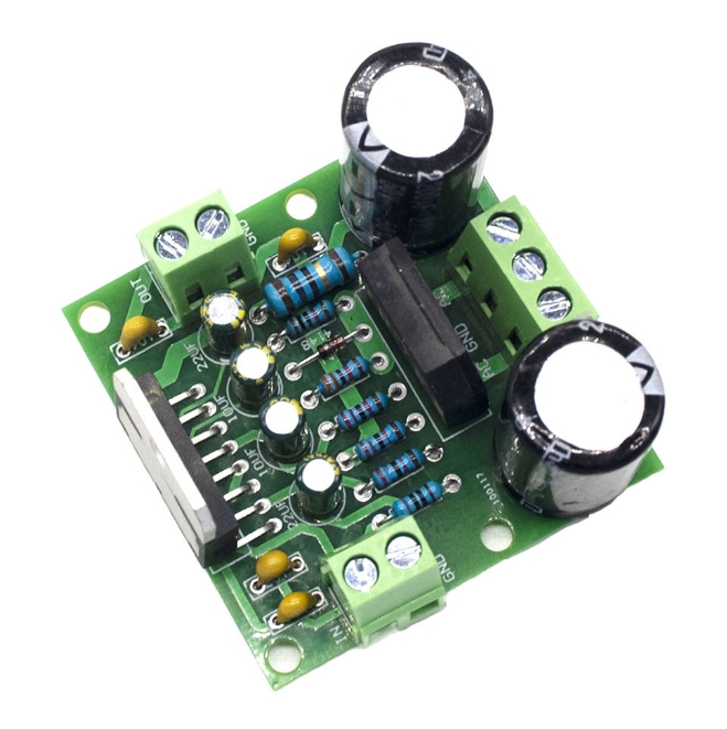
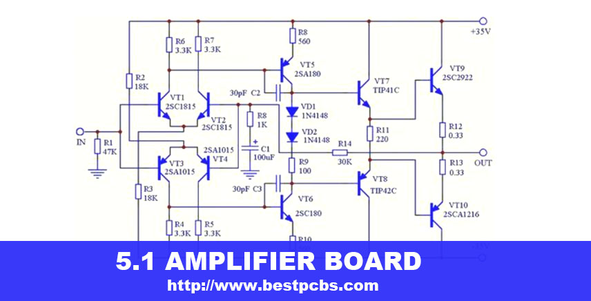
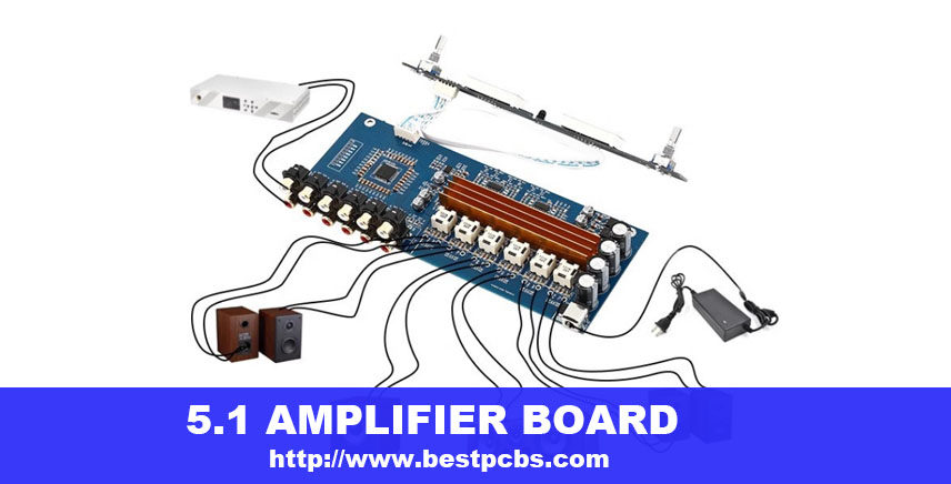
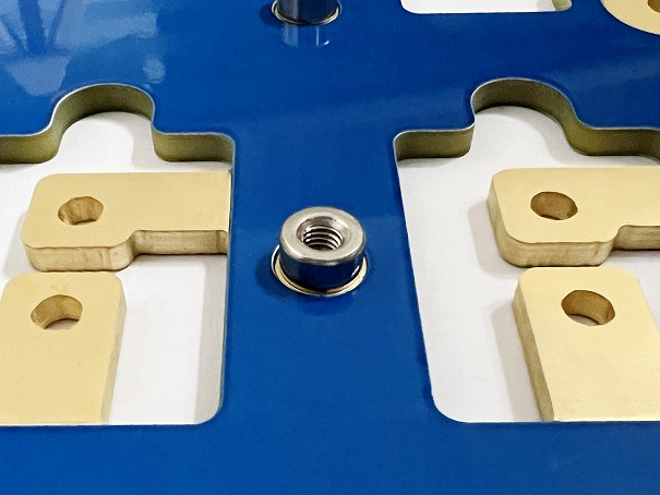
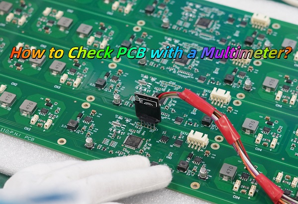
pcb support metallic are mainly used to support and fix circuit boards to ensure their stability and reliability. The following is a summary of the materials and types, functions and uses of PCB metal support columns, as well as their market supply.
Materials and types:
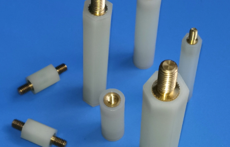
1.The materials are mainly brass, stainless steel and other metals, which have good conductivity and corrosion resistance.
2.Types include hexagonal double-pass copper columns, single-head isolation copper columns, external hexagonal PCB metal external thread spacing screw columns, etc.
Functions and uses:
1.Support and fix circuit boards to prevent them from moving or deforming during use.
2.Provide circuit connection points to achieve electrical connection between circuit boards.
Market supply:
1.There are many suppliers in the market that provide PCB metal support columns of different specifications and materials.
2.Suppliers usually provide customized services to meet the specific needs of customers.
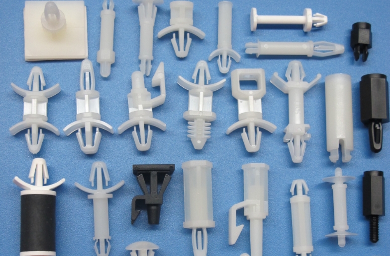
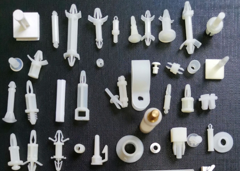
What is a PCB support column
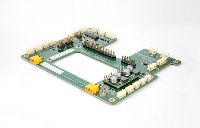
PCB support columns, also known as circuit board support columns, are mainly used to support and connect circuit boards and are widely used in computer connectors, various PCB assemblies, and electronics. These support columns are usually made of insulating materials such as plastic and nylon, and have good insulation properties and mechanical strength. They have various designs, including aircraft type, flat bottom type, hexagonal type, and other shapes to meet different installation and usage requirements.
Function of PCB support column
PCB support columns play an important role in multiple application scenarios.
To ensure the stability and reliability of PCB in various application scenarios, the support columns are used to support and position the sub-board, ensure that the sub-board is placed flat on the carrier, and thus improve the welding effect between the sub-board and the carrier. In the injection mold, the support column supports the B plate to prevent it from being deformed by pressure during injection molding. In the design of large-load electric cylinders, the support column plays a role in enhancing structural strength, improving pressure resistance, optimizing load capacity, maintaining accuracy and stability, and extending service life.
In addition, in the communication engineering PCB welding and docking support device, the support column is used to clamp and fix the docking plug to ensure that the communication engineering PCB can be stably docked and welded.
In summary, the main function of the PCB support column is to provide stable support and positioning to ensure the stability and reliability of the PCB in various application scenarios.
How to choose PCB support columns?
Choosing a suitable PCB support column requires comprehensive consideration of multiple factors such as performance, material, size, and cost
1.Performance requirements: Determine the performance required by the support column according to the application scenario, such as load-bearing capacity, corrosion resistance, and high temperature resistance.
2.Material selection: Common materials include metal, plastic, etc. Metal support columns are strong and durable, but may be susceptible to corrosion; plastic support columns are light and have good insulation, but may not be strong enough.
3.Size and shape: The size and shape of the support column should match the specifications and installation requirements of the PCB to ensure stable support and connection.
4.Cost and budget: Under the premise of meeting performance requirements, consider the cost and budget of the support column and choose a cost-effective product
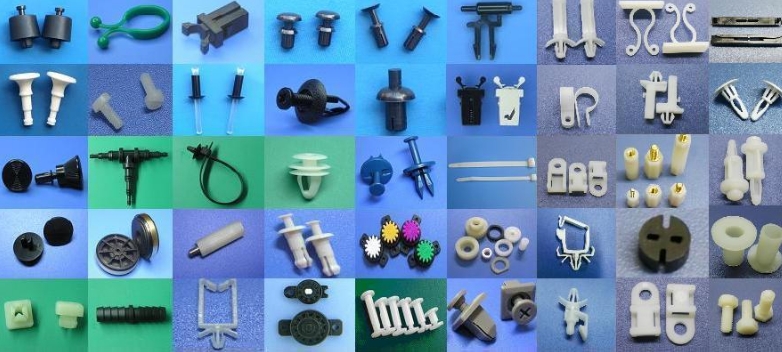
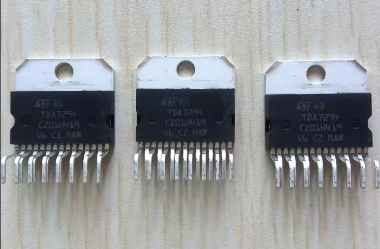
PCB support column material?
PCB support columns are widely used in the electronics field. They are mainly used to support and connect circuit boards. Common PCB support column materials include nylon, plastic, metal (such as brass, stainless steel, aluminum) and resin, etc. Nylon and plastic are the most commonly used materials due to their good insulation performance, easy processing and low cost. Metal materials such as brass and stainless steel are selected in certain specific applications due to their good mechanical strength and conductivity. Resin materials are also used in the production of some PCB support columns due to their insulation and processing properties.