pcb
Home > Blog

What is Thermal-Electric Separation Copper Substrate with Flexible PCB?

August 3rd, 2024

As electronic devices become increasingly miniaturized and high-performance, traditional circuit boards are no longer sufficient for certain high-demand applications. To address these challenges, the Thermal-Electric Separation Copper Substrate with Flexible PCB has emerged. This innovative composite circuit board combines the efficient heat dissipation characteristics of thermal-electric separation copper substrates with the flexibility of flexible PCBs (FPC). It is widely use for high-performance electronic products, which requires efficient heat dissipation and complex circuit.

What is Thermal-Electric Separation Copper Substrate with Flexible PCB?

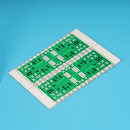
The Thermal-Electric Separation Copper Substrate with Flexible PCB is a composite material that combines a rigid thermal-electric separation copper substrate with a flexible circuit board. It integrates the advantages of both, providing superior performance in high-power and high-density applications.

What is Thermal-Electric Separation Copper Substrate with Flexible PCB?

1. Thermal-Electric Separation Copper Substrate

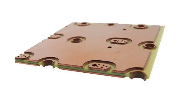
The thermal-electric separation copper substrate is designed for high-power electronic devices, providing an efficient heat dissipation solution. It separates the paths of heat and electrical signals to avoid thermal interference with electrical performance. Its structure typically includes:

  • Single-sided design: Electronic components are placed on one side of the copper substrate, while the other side is used for heat dissipation.
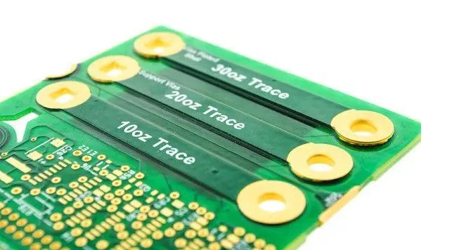
  • High thermal conductivity materials: Such as copper or aluminum, which can quickly conduct heat, like copper is 400W/m.k, aluminum is 237W/m.k.
  • Thermal vias: Vertical heat conduction paths that rapidly transfer heat to the dissipation layer.

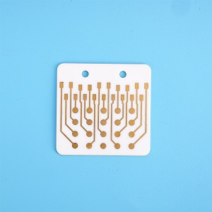
2. Flexible PCB (FPC)

Flexible PCBs (Flexible Printed Circuits, FPC) use flexible materials like polyimide (PI) or polyester (PET) that can bend and fold to adapt to complex three-dimensional structures and dynamic application scenarios. Their advantages include:

  • Lightweight: Reducing the overall weight of the device.
  • High-density wiring: Achieving complex circuit designs in limited space.
  • Flexibility: Meeting diverse design needs.

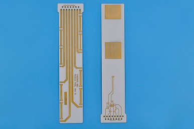
Structure and Characteristics

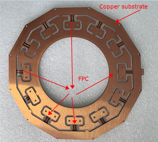
The structure of the Thermal-Electric Separation Copper Substrate with Flexible PCB includes rigid and flexible parts, connected together using conductive adhesives or other bonding materials to form a unified whole.

1. Rigid Part

The rigid part uses the thermal-electric separation copper substrate, responsible for efficient heat dissipation and mechanical support. This part usually carries high-power components to ensure rapid heat transfer and dissipation.

2. Flexible Part

The flexible part uses the flexible PCB, which can bend and fold to fit the complex internal structure of devices. This part is typically used to connect the rigid part with other modules that require flexible connections.

3. Bonding Method

The flexible and rigid parts are bonded together using conductive adhesives, welding, or mechanical connections. The design of the bonding area ensures stable electrical connections and reliability during bending and dynamic use.

Thermal-Electric Separation Copper Substrate with Flexible PCB Advantages

1. Efficient Heat Dissipation

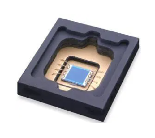
The thermal-electric separation copper substrate provides excellent heat dissipation, effectively conducting away the heat generated by high-power components to maintain a reasonable operating temperature range. This is especially important for applications like high-power LEDs and power semiconductor devices.

2. Flexibility

The use of the flexible PCB offers great design freedom, allowing adaptation to the complex three-dimensional structures and dynamic application needs within devices. This enables designers to achieve more complex circuit designs in limited spaces, increasing device integration and functionality.

3. Reliability

The thermal-electric separation design and high thermal conductivity materials enhance the reliability of the circuit board, reducing the impact of heat on electrical performance. The flexible part reduces the number of connection points, lowering the risk of failure.

4. Space Saving

Combining the advantages of rigid and flexible circuit boards allows for efficient heat dissipation and complex circuit in limited space. This is crucial for modern miniaturized and high-density electronic product designs.

Where Thermal-Electric Separation Copper Substrate with Flexible PCB used?

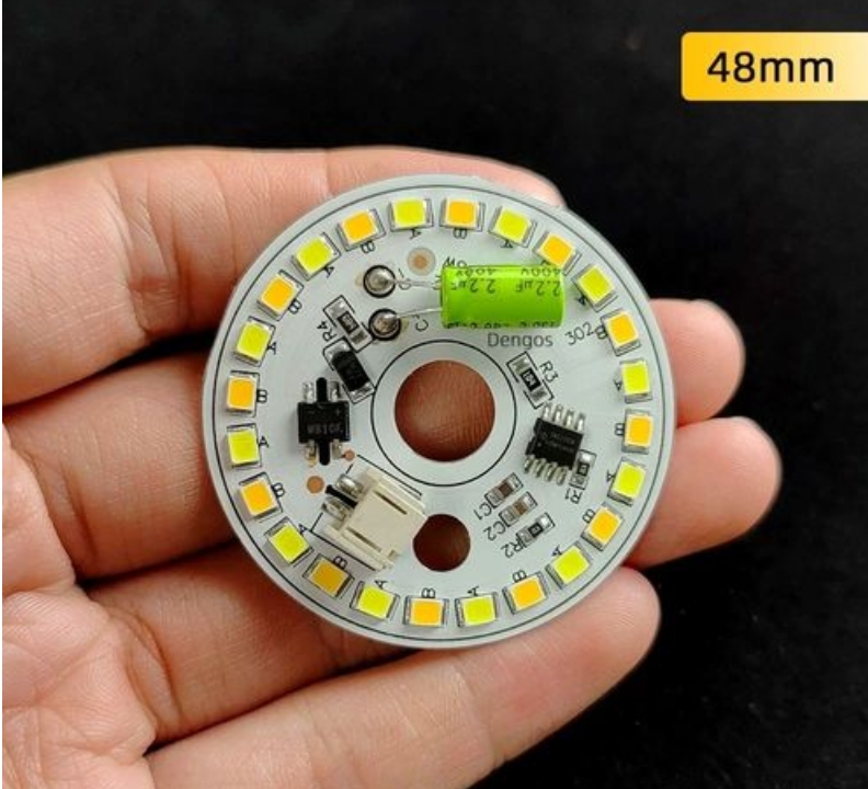
1. High-Power LED Lighting

High-power LEDs generate a significant amount of heat during operation. The thermal-electric separation copper substrate provides an efficient heat dissipation solution, ensuring the stable operation and long lifespan of LEDs. The flexible part is used to connect different LED modules, accommodating diverse design requirements.

2. Automotive Electronics

In automotive electronics, such as in-vehicle cameras and sensor modules, efficient heat dissipation and compact design are required. The thermal-electric separation copper substrate with flexible PCB can meet these demands, enhancing device reliability and performance.

What is Thermal-Electric Separation Copper Substrate with Flexible PCB?

3. Consumer Electronics

Devices like smartphones and tablets require lightweight and miniaturized designs. The thermal-electric separation copper substrate with flexible PCB offers efficient heat dissipation and flexible circuit, optimizing device performance and user experience.

4. Medical Devices

In applications that require flexibility and reliability, such as portable diagnostic equipment and implantable medical devices, the thermal-electric separation copper substrate with flexible PCB can help to enhancing device performance and reliability.

How does Thermal-Electric Separation Copper Substrate with Flexible PCB manufactured?

The manufacturing process for the thermal-electric separation copper substrate with flexible PCB is complex, typically including the following steps:

  1. Material Preparation: Selecting appropriate rigid and flexible materials and performing pre-treatment.
  2. Circuit Printing: Printing circuit patterns on both rigid and flexible materials.
  3. Lamination and Bonding: Combining the flexible circuit board with the thermal-electric separation copper substrate, usually using conductive adhesives or other bonding materials.
  4. Drilling and Plating: Drilling holes and electroplating to form conductive paths on the combined board.
  5. Surface Treatment: Performing surface treatments such as pad coating on the circuit board.
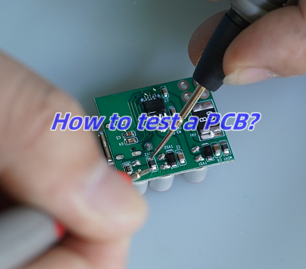
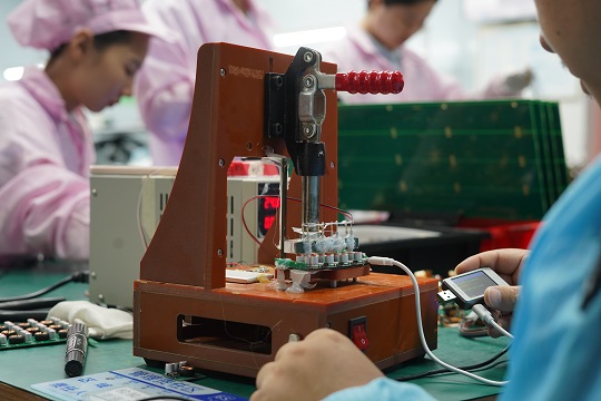
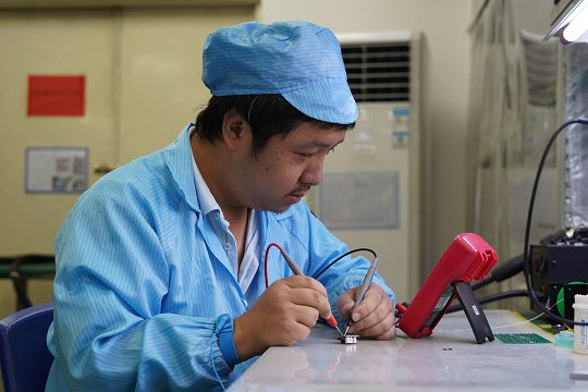
  6. Testing and Inspection: Conducting electrical and mechanical performance tests to ensure the quality and reliability of the board.

The thermal-electric separation copper substrate with flexible PCB, as an innovative composite circuit board, combines the advantages of efficient heat dissipation and flexible wiring. It is widely used in high-performance and complex design electronic products. With continuous technological advancements and growing market demand, this composite circuit board will play an important role in more fields, driving the ongoing innovation of electronic manufacturing technology. Want know more about it, just feel your free to contact us.

hs code electronic,What is the HS code for circuit boards?

August 2nd, 2024

hs code electronic (HS codes) for electronic products involve multiple categories and specific commodities, including but not limited to laptops, tablets, portable devices, phones, electronic watches, smartphones, electronic game consoles, electric toys, electronic cigarettes, etc. The HS codes for these commodities are as follows:

The HS code for laptops and tablets is 8471301000.
The HS code for portable devices is 8471309000.
The HS code for phones is 8517129000.
The HS code for electronic watches is 9102190000.
The HS code for smartphones is 8517130000.
The HS code for electronic game consoles is 9504901000.
The HS code for electric toys is 8501101000.
The HS code for electronic cigarettes is 8516799000. ‌
The HS code for PCB (printed circuit board) is 8534001000.
PCBs made of FR-4 material (i.e. silicon tetrachloride fiberglass board) are classified under HS code 8534.00.00
HS code for integrated circuit and microelectronic component parts is 8542900000
Electronic circuit boards: HS code is 8534.00.00
Capacitors: HS code is 8532.10.00
Resistors: HS code is 8533.10.00
Transistors: HS code is 8541.10.00
Integrated circuits: HS code is 8542.31.00
Connectors: HS code is 8536.69.00

These HS codes are the standards used by customs to classify and count goods in international trade. Each commodity has a specific HS code to facilitate customs management and statistics of imported and exported goods. ‌Knowing these codes is very important for companies and individuals engaged in international trade, as it can help them declare goods correctly and avoid mistakes in tariffs or customs declarations.

How do I find an HS code?

You’ll often find HS codes on invoices and shipping documents around the world. HTS codes are like Schedule B numbers, but for importing goods into the United States instead. They’re also made up of 10 digits, and they help the US government to track imports and apply the right tariffs to different products.

How do I find an HS code?

HS code is a coding system consisting of six digits, each of which represents specific information in order to accurately define and classify goods. The following is the basic structure of HS code:

The first digit (chapter): represents the major category of goods, usually describing the general nature of the goods, such as raw materials, machinery and equipment, electronic products, etc.

The second digit (section): further subdivides the major category of the first digit to provide more specific information.

The third digit (subsection): continues to refine the classification of goods, usually including the materials and uses of goods.

The fourth digit (group): describes the specific characteristics and attributes of the goods.

The fifth digit (subgroup): provides more specific information related to the characteristics of the goods.

The sixth digit (item): the most specific code, used to identify specific goods.

What is the HS code for circuit boards?

he HS code for circuit boards is a standard international commodity code, the full name of which is “HS code for printed circuit boards”, which is part of the customs coding system. The coding system was formulated by the World Customs Organization (WCO) to uniformly identify the classification and classification of international goods.

The role of the HS code for circuit boards

The HS code for circuit boards is an important voucher in international trade, which can help customs to quickly and accurately count and classify imported or exported goods. At the same time, it is also an important basis for customs to determine tariff rates, levy import tariffs, supervise trade measures, and implement regional protectionist policies.

Classification of HS codes for circuit boards

According to WCO regulations, the HS code for circuit boards is divided into 16 chapters, Chapters 1 to 5 are industrial product codes, Chapters 6 to 14 are agricultural product codes, Chapter 15 is unlisted commodity codes, and Chapter 16 is supplementary codes for machinery and equipment. Among them, the HS code classification of circuit boards is in Chapter 85, which belongs to machinery and electrical equipment.

Application of HS code of circuit boards


HS code of circuit boards is one of the key points in international trade. Reasonable coding will have an important impact on trade costs and trade efficiency. When conducting import and export trade activities of circuit boards, relevant HS codes must be correctly declared, otherwise they may face customs control, return, fines and other consequences. Therefore, the correct understanding and application of HS code of circuit boards is of great significance to the commercial success of enterprises.

As a basic work in international trade, HS code of circuit boards not only plays an important role in facilitating and smooth trade, saving costs and improving efficiency, but also is a key link in the import and export trade of circuit boards. Therefore, enterprises should attach great importance to the correct understanding and application of HS code of circuit boards, making it a powerful tool to promote the development of enterprises.

What Is led ring light pcb

August 2nd, 2024

led ring light pcb leads the development of lighting industry with its innovative design, high efficiency and flexibility, bringing more intelligent and comfortable lighting experience to our life.

It is not only an integrated platform of electronic components, but also a perfect combination of modern technology and aesthetics, and is the focus of future lighting trends.

led ring light pcb, like a magic wand on the electronic stage, uses precise SMT technology to lightly attach LED components to it. Whether it is a warm small lamp for home decoration, efficient lighting in commercial space, or smart display inside the car, it is indispensable.

Its core structure includes efficient LED lamp beads, power cords that provide electricity, and intelligent controllers that adjust light effects, which together build an excellent lighting solution.

What Is led ring light pcb

Why use mcpcb for led ring light pcb

With the continuous development of LED technology, the heat generated by LEDs has gradually increased. The traditional FR4 printed circuit board (PCB) has been unable to meet the heat dissipation requirements due to its low thermal conductivity (only 0.36W/m.K). In order to solve this problem, the metal core printed circuit board (MCPCB) was proposed. It attaches the original printed circuit board to a metal with better thermal conductivity (such as aluminum and copper) to enhance the heat dissipation effect. The thermal conductivity efficiency of MCPCB is higher than that of traditional FR4 PCB, reaching 1W/m.K to 2.2W/m.K, which effectively improves the heat dissipation performance of LED PCB.

In addition, the use of MCPCB can also reduce the number of LEDs required to generate lighting, making it an ideal choice for street lights, automotive LED applications, and backlight unit applications. The use of metal substrates has practical advantages in heat dissipation, thermal conductivity, reliability, and electrical insulation, especially in harsh environments, and can also achieve reliable operation of LEDs. For example, using a metal substrate can reduce the LED junction temperature by 20-30°C, improve light output and enhance the overall performance of the product, ensure consistent UV light generation, and expand the possibilities of UV applications in various industries.

Unveiling the Components of LED PCBs

  • LED Chips: The heart of the LED PCB, these semiconductor chips emit light when current passes through them.
  • Substrate Material: The base layer of the PCB provides mechanical support and thermal conductivity.
  • Copper Traces: These conductive pathways connect the LEDs and other components, allowing current to flow through the circuit.
  • Solder Mask: A protective layer that covers the copper traces, safeguarding them from external factors and preventing short circuits.
  • Silkscreen: This layer contains markings and labels, providing important information about the PCB’s components and assembly.

Advantages of led ring light pcb?

Thermal performance advantages of metal substrate PCB

High thermal conductivity:
The thermal conductivity of metal substrate PCB is much better than that of traditional plastic substrates such as FR4. It can effectively conduct the heat generated by components, reduce the operating temperature of components, and improve the reliability and life of circuit boards.

Good thermal stability:
Metal substrate PCB can maintain good dimensional stability and electrical performance in high temperature environment, and is suitable for high temperature working environment.

Mechanical performance advantages of metal substrate PCB

High strength: Metal substrate PCB has high mechanical strength and rigidity, is not easy to deform and break, and can withstand large external forces and vibrations.

Good processability: Metal substrate PCB can be processed by conventional mechanical processing methods such as drilling and cutting, which is convenient for the production of circuit boards with complex shapes and sizes.

Electrical performance advantages of metal substrate PCB
Excellent electrical insulation performance: Metal substrate PCB has a special insulation layer design to ensure good electrical insulation performance and avoid electrical short circuits between components.

Low impedance: The conductive layer of metal substrate PCB is made of metal material, which has low impedance, which is conducive to signal transmission and processing.

How does led ring light pcb dissipate heat?

The power device is mounted on the circuit layer. The heat generated by the device during operation is quickly transferred to the metal base layer through the insulating layer, and then the metal base layer transfers the heat to achieve heat dissipation of the device.

Compared with the traditional FR-4, the aluminum substrate can reduce the thermal resistance to the minimum, making the aluminum substrate have excellent thermal conductivity; compared with the thick film ceramic circuit, its mechanical properties are extremely good.

In the circuit design scheme, the heat diffusion is handled very effectively, thereby reducing the module operating temperature, extending the service life, and improving the power density and reliability; reducing the assembly of the heat sink and other hardware (including thermal interface materials), reducing the product volume, and reducing the hardware and assembly costs; combining the power circuit and the control circuit

How to make a LED light circuit board?

Step 1: Design Your LED PCB:
Using PCB design software, create a schematic for your LED circuit and design the PCB layout, considering component placement and signal flow.

Step 2: Choose the Materials:
Select a suitable substrate material and copper-clad board based on your project requirements.

Step 3: Transfer the Design:
Print your PCB layout onto a special transfer paper and transfer it onto the copper-clad board using a heat press.

Step 4: Etch the Board:
Immerse the board in an etching solution to remove the excess copper and reveal the copper traces.

Step 5: Drill Holes:
Drill holes on the board to accommodate the LED chips and other components.

Step 6: Solder the Components:
Carefully solder the LED chips and other components onto the board, ensuring secure connections.

Step 7: Test Your LED PCB:
Connect your LED PCB to a power source and test the LEDs to ensure they light up correctly.

How to make a LED light circuit board?

Capabilities of led ring light pcb?

ItemCapabilities
Layer Count1 – 10 Layers
Max Board Dimension24*64″(610*1625mm)
Min Board Thickness0.6mm
Max Board Thickness4.0mm
Conductor Thickness0.5oz – 10oz
Min Line Width/Line Space4/4mil (0.10/0.10mm)
Min Hole Diameter10mil (0.25mm)
Min Punch Hole Dia0.12″ (3.0mm)
Min Hole Spacing16mil (0.4mm)
Min PAD Ring(Single)3mil (0.075mm)
PTH Wall ThicknessNormal: 0.59mil (15um); HDI: 0.48mil (12um)
Min Solder PAD Dia14mil (0.35mm)
Min Soldermask Bridge8mil (0.20mm)
Min BAG PAD Margin5mil (0.125mm)
PTH/NPTH Dia TolerancePTH: ±3 mil (0.075mm); NPTH: ±2mil (0.05mm)
Hole Position Deviation±3mil (0.075mm)
Outline ToleranceCNC: ±6 mil (0.15mm); Die Punch: ±6 mil (0.1mm)
Max Aspect Ratio10:01
Surface TreatmentENIG, Flash Gold, Hard Gold Finger, Gold Plating(50mil), Gold finger,
Selected Gold Plating, ENEPIG, ENIPIG, HAL, HASL(LF), OSP, Silver Imm., Tin Imm
Capabilities

Applications of led ring light pcb?

  1. Application in medical equipment
    The rapid progress of medicine is closely related to the rapid development of the electronics industry. Many medical devices are made of basic PCBs alone, such as pH meters, heart rate sensors, temperature measurements, electrocardiographs, electroencephalographs, MRIs, X-ray machines, CT scanners, blood pressure machines, blood sugar level measuring equipment, etc.
  2. Application in industrial equipment
    PCBs are widely used in manufacturing, especially in industries with high-power mechanical equipment; these devices run on high power and require high current circuit drive. Such as arc welding, large servo motor drives, lead-acid battery chargers, clothing cotton machines, etc.
  3. Application in lighting
    LED lights and high-intensity LEDs are mounted on PCBs based on aluminum substrates; aluminum has the property of absorbing heat and dissipating it in the air.
  4. Application in the automotive and aerospace industries
    Flexible PCBs are lightweight but can withstand high vibrations. Because of their light weight, they can reduce the total weight of spacecraft; flexible PCBs can be adjusted even in narrow spaces. These flexible PCBs are used as connectors, interfaces, and can be assembled even in compact spaces

FAQs About led ring light pcb

What is the thermal conductivities and withstanding voltages of BT/FR4 layer and Dielectric layer?
The SinkPAD conducts heat primarily through the copper base (400W/m.K), the withstanding voltages of Dielectric layer is around 4KV.

What is the placement accuracy for the SMT components?
+/-0.05mm is our SMT accuracy tolerance. You are welcome to come to our SMT factory in Shenzhen China and Vietnam.

Can the aluminum be made as the base of sinkpad MCPCB?

Actually, the sinkpad can only use copper as the base.
As you can see the below manufacturing steps, the SinkPad will etch the copper base into convex platform with Copper Etching Solution, then hollow out the Double Layer FR4 PCB, and do lamination with the convex platform.
However, regarding of current technical conditions, since aluminum or aluminum alloy cannot directly react with acid, the reaction process is too complex and difficult to control, which will increase the difficulty of etching the LED pad platform. Considering the scrap rate, the process of etching LED pad platform with aluminum is more complex and the overall cost is higher.

Can I plated copper in mcpcb via holes?
Generally speaking, copper plating through holes requires hole rings, otherwise the copper in the hole wall will easily fall off.

In addition, if it is a copper substrate, through the hole first to resin plug before copper plating. 

Otherwise there’s no chemical reaction between copper and copper. And if the copper layer is connected to each copper layer, it is easy to short circuit.

Are you UL certified led pcb manufacturer?

Yes, we are UL certified manufacturer, our UL is E475635. We have already passed UL certificated. Meanwhile, we are passed ISO9001, ISO13485 and IATF16949 certifications. 

Our LED pcbs are manufactured under highly monitored by these quality system controls.

How does the conveity of sinkpad manufactured?

Actually the sinkpad can only use copper as the base.

As you can see the below manufacturing steps, the SinkPad will etch the copper base into convex platform with Copper Etching Solution, then hollow out the Double Layer FR4 PCB, and do lamination with the convex platform.However, regarding of current technical conditions, since aluminum or aluminum alloy cannot directly react with acid, the reaction process is too complex and difficult to control, which will increase the difficulty of etching.

What Is led light pcb?

August 2nd, 2024

led light pcb , or printed circuit board, is a stable carrier of electronic components. It not only realizes electrical connection but also plays a supporting role. As the core component of electronic products, it is widely used in various electronic devices. In the field of LED lighting, PCB light board provides support and power for LED lamp beads, ensuring their stable operation in scenes such as home, commercial and automotive lighting. PCB with LED is often used to manufacture electronic products such as indicator lights, lighting equipment and display screens. The LED lamp beads on these PCBs are usually precisely soldered by SMT (surface mount technology).

What Is led light pcb?

led light pcb

LED PCB light board leads the development of the lighting industry with its innovative design, high efficiency and flexibility, bringing a more intelligent and comfortable lighting experience to our lives. It is not only an integrated platform for electronic components, but also a perfect combination of modern technology and aesthetics, and is the focus of future lighting trends.

Why use mcpcb for led light pcb

With the continuous development of LED technology, the heat generated by LEDs has gradually increased. The traditional FR4 printed circuit board (PCB) has been unable to meet the heat dissipation requirements due to its low thermal conductivity (only 0.36W/m.K). In order to solve this problem, the metal core printed circuit board (MCPCB) was proposed. It attaches the original printed circuit board to a metal with better thermal conductivity (such as aluminum and copper) to enhance the heat dissipation effect. The thermal conductivity efficiency of MCPCB is higher than that of traditional FR4 PCB, reaching 1W/m.K to 2.2W/m.K, which effectively improves the heat dissipation performance of LED PCB.

In addition, the use of MCPCB can also reduce the number of LEDs required to generate lighting, making it an ideal choice for street lights, automotive LED applications, and backlight unit applications. The use of metal substrates has practical advantages in heat dissipation, thermal conductivity, reliability, and electrical insulation, especially in harsh environments, and can also achieve reliable operation of LEDs. For example, using a metal substrate can reduce the LED junction temperature by 20-30°C, improve light output and enhance the overall performance of the product, ensure consistent UV light generation, and expand the possibilities of UV applications in various industries.

Why use mcpcb for led light pcb

Why use mcpcb for led light pcb

Advantages of led light pcb?

High thermal conductivity: LED PCB, especially aluminum substrate, uses aluminum alloy material with high thermal conductivity, which can effectively conduct away the heat generated by LED, maintain the stability of LED operation and extend the service life. This high thermal conductivity is essential to prevent heat accumulation and keep LED working at high brightness for a long time.

High efficiency: Compared with traditional incandescent lamps and energy-saving lamps, LED lamps have higher luminous efficiency and can provide better lighting effects while reducing energy consumption. This makes LED PCB have significant advantages in energy saving and environmental protection.

Long life: The service life of LED PCB far exceeds that of traditional lighting products, and it can provide longer continuous lighting, reducing the trouble of frequent bulb replacement and reducing maintenance costs.

Low energy consumption: LED PCB requires much less electricity than traditional lighting equipment while providing the same brightness, which is very important for energy saving, emission reduction and sustainable development

How does led light pcb dissipate heat?

The power device is mounted on the circuit layer. The heat generated by the device during operation is quickly transferred to the metal base layer through the insulating layer, and then the metal base layer transfers the heat to achieve heat dissipation of the device. Compared with the traditional FR-4, the aluminum substrate can reduce the thermal resistance to the minimum, making the aluminum substrate have excellent thermal conductivity; compared with the thick film ceramic circuit, its mechanical properties are extremely good. In the circuit design scheme, the heat diffusion is handled very effectively, thereby reducing the module operating temperature, extending the service life, and improving the power density and reliability; reducing the assembly of the heat sink and other hardware (including thermal interface materials), reducing the product volume, and reducing the hardware and assembly costs; combining the power circuit and the control circuit

How to make a LED light circuit board?

  1. Cutting
  2. Cutting process Picking materials – cutting
  3. The purpose of cutting
    Cut the large-sized incoming materials into the size required for production
  4. Precautions for cutting
    ① Check the size of the first piece of material
    ② Pay attention to the scratches on the aluminum surface and the copper surface
    ③ Pay attention to the delamination and flash of the board edge
  5. Drilling
  6. Drilling process
    Pinning – drilling – board inspection
  7. The purpose of drilling
    Positioning and drilling holes in the board to assist the subsequent production process and customer assembly
  8. Precautions for drilling
    ① Check the number of holes and the size of the holes
    ② Avoid scratches on the board
    ③ Check the flash of the aluminum surface and the hole position deviation
    ④ Check and replace the drill bit in time
    ⑤ Drilling is divided into two stages, one drilling: drilling holes after cutting for peripheral tool holes
    Second drilling: tool holes in the unit after solder mask
  9. Dry/wet film imaging
  10. Dry/wet film imaging process
    Grinding board – film pasting – exposure – development
  11. Purpose of dry/wet film imaging
    To present the part required for making circuits on the board
  12. Precautions for dry/wet film imaging
    ① Check whether the circuit is open after development
    ② Whether the development alignment is biased to prevent the generation of dry film fragments
    ③ Pay attention to the circuit defects caused by scratches on the board
    ④ No air should remain during exposure to prevent poor exposure
    ⑤ After exposure, it should be still for more than 15 minutes before development
    IV. Acid/alkaline etching
  13. Acid/alkaline etching process
    Etching-film stripping-drying-board inspection
  14. Purpose of acid/alkaline etching
    After imaging the dry/wet film, keep the required circuit part and remove the excess part outside the circuit. During acid etching, attention should be paid to the corrosion of the etching solution to the aluminum substrate;
  15. Precautions for acid/alkaline etching
    ① Pay attention to incomplete etching and excessive etching
    ② Pay attention to line width and line thickness
    ③ Oxidation and scratches are not allowed on the copper surface
    ④ The dry film should be removed cleanly
    V. Silk screen solder mask and characters
  16. Silk screen solder mask and character process
    Silk screen-pre-bake-exposure-development-characters
  17. Purpose of silk screen solder mask and characters
    ① Anti-soldering: protect circuits that do not need soldering and prevent tin from entering and causing short circuits
    ② Characters: serve as markings
  18. Precautions for silk screen solder mask and characters
    ① Check whether there is garbage or foreign matter on the board
    ② Check the cleanliness of the stencil ③ Pre-bake for more than 30 minutes after silk screen printing to avoid bubbles in the circuit
    ④ Pay attention to the thickness and uniformity of the silk screen
    ⑤ After pre-bake, the board should be completely cooled to avoid film contamination or damage to the glossiness of the ink surface
    ⑥ Place the ink side down during development
    VI. V-CUT, gong board
  19. V-CUT, gong board process
    V-CUT——gong board——tear protective film——remove burrs
  20. Purpose of V-CUT, gong board
    ① V-CUT: Cut the single PCS circuit and the entire PNL board to leave a small part connected for easy packaging and removal
    ② Gong board: remove the excess part of the circuit board
  21. Precautions for V-CUT, gong board
    ① During the V-CUT process, pay attention to the size of the V, the incompleteness and burrs of the edges
    ② Pay attention to the burrs caused by the gong board, the gong knife is tilted, and the gong knife is checked and replaced in time
    ③ Finally, avoid scratches on the board when removing the burr
    VII. Testing, OSP
  22. Testing, OSP process
    Circuit test-voltage resistance test-OSP
  23. Testing, the purpose of OSP
    ① Circuit test: Check whether the completed circuit is working normally
    ② Voltage resistance test: Check whether the completed circuit can withstand the specified voltage environment
    ③ OSP: Allow the circuit to be soldered better
  24. Testing, OSP precautions
    ① How to distinguish and store qualified and unqualified products after testing
    ② Placement after OSP
    ③ Avoid damage to the circuit
    VIII. FQC, FQA, packaging, shipment
  25. Process
    FQC-FQA-packaging-shipping
  26. Purpose
    ① FQC conducts full inspection and confirmation of the product
    ② FQA spot check and verification
    ③ Pack and ship to customers as required
  27. Note
    ① FQC should pay attention to the appearance confirmation during the visual inspection and make reasonable distinctions
    ② FQA should conduct random inspections to verify the inspection standards of FQC
    ③ Confirm the packaging quantity to avoid mixed boards, wrong boards and packaging damage

Capabilities of led light pcb?

ItemCapabilities
Layer Count1 – 10 Layers
Max Board Dimension24*64″(610*1625mm)
Min Board Thickness0.6mm
Max Board Thickness4.0mm
Conductor Thickness0.5oz – 10oz
Min Line Width/Line Space4/4mil (0.10/0.10mm)
Min Hole Diameter10mil (0.25mm)
Min Punch Hole Dia0.12″ (3.0mm)
Min Hole Spacing16mil (0.4mm)
Min PAD Ring(Single)3mil (0.075mm)
PTH Wall ThicknessNormal: 0.59mil (15um); HDI: 0.48mil (12um)
Min Solder PAD Dia14mil (0.35mm)
Min Soldermask Bridge8mil (0.20mm)
Min BAG PAD Margin5mil (0.125mm)
PTH/NPTH Dia TolerancePTH: ±3 mil (0.075mm); NPTH: ±2mil (0.05mm)
Hole Position Deviation±3mil (0.075mm)
Outline ToleranceCNC: ±6 mil (0.15mm); Die Punch: ±6 mil (0.1mm)
Max Aspect Ratio10:01
Surface TreatmentENIG, Flash Gold, Hard Gold Finger, Gold Plating(50mil), Gold finger,
Selected Gold Plating, ENEPIG, ENIPIG, HAL, HASL(LF), OSP, Silver Imm., Tin Imm

Applications of led light pcb?

  1. Application in medical equipment
    The rapid progress of medicine is closely related to the rapid development of the electronics industry. Many medical devices are made of basic PCBs alone, such as pH meters, heart rate sensors, temperature measurements, electrocardiographs, electroencephalographs, MRIs, X-ray machines, CT scanners, blood pressure machines, blood sugar level measuring equipment, etc.
  2. Application in industrial equipment
    PCBs are widely used in manufacturing, especially in industries with high-power mechanical equipment; these devices run on high power and require high current circuit drive. Such as arc welding, large servo motor drives, lead-acid battery chargers, clothing cotton machines, etc.
  3. Application in lighting
    LED lights and high-intensity LEDs are mounted on PCBs based on aluminum substrates; aluminum has the property of absorbing heat and dissipating it in the air.
  4. Application in the automotive and aerospace industries
    Flexible PCBs are lightweight but can withstand high vibrations. Because of their light weight, they can reduce the total weight of spacecraft; flexible PCBs can be adjusted even in narrow spaces. These flexible PCBs are used as connectors, interfaces, and can be assembled even in compact spaces

How to Test a PCB Board? – Best Technology

August 2nd, 2024

Nowadays, PCBs became more and more important and you can see it in every electronic device. The PCB plays a critical role in our daily life. With circuit board, the device can power on and help to transmit signals, manage heat and perform electricity. A good PCB can help to improve the overall of your device. However, not all the PCBs are work good and within your expectable, you must know how to test it and ensure it enables a good performance. As an experienced PCB manufacturers in Asia, today we want to share with you how we test a PCB, and we try to use simple words to make you sense.

How to Test a PCB? - Best Technology

What is a printed circuit board?

Before knowing the methods of testing circuit board, let’s understand the definition of PCB. A PCB is a flat board made from insulating materials like fiber glasses with conductive pathways etched onto its surface. The pathways we called circuit or traces. These pathways connect different electronic components, so that they can communicate and function together. PCBs come in various materials, shapes and sizes, which always is customized to meet specific applications and performance requirements.

PCBs can be divided into different types according to substrate material used. They are – normal FR4 PCB, polyimide flexible PCB, metal core PCB, ceramic PCB, rogers PCB. Different has its own properties and advantages. The choice of materials and the design of the PCB significantly impact the performance and reliability of the final product. Understanding the materials used in PCBs is crucial for anyone involved in electronics, from hobbyists to professional engineers/designers.

How to Test a PCB? - Best Technology

Common PCB Circuit Board Issues

Though PCB has a strong construction, they are easy to be broken or failure since they always encounter a range of issues. These problems can stem from manufacturing defects, wear and tear, or improper handling. Identifying and diagnosing these issues promptly is crucial for maintaining the reliability and performance of electronic devices. Common issues we faced are including:

  • Open Circuits: These occur when a break in the circuits prevents current flow normally. Open circuits can result from physical damage or manufacturing errors.
  • Short Circuits: Due to improper soldering, unreasonable circuit design and other reasons, resulting in a short circuit between two or more points in the circuit that should not be connected. This can cause excessive current flow, potentially damaging components.
  • Grounding: The unreasonable design of ground area leads to interference signals on the grounding, which affects the normal operation of the circuit.
  • Signal: The signal circuit design is not reasonable, resulting in interference signals on the signal.
  • Component Failures: Individual components on a PCB can fail due to aging, overheating, or electrical stress breakdown. And incorrect orientation will lead to the failure of PCB.
  • Soldering Issues: Poor soldering can lead to weak connections, causing intermittent faults or complete circuit failure. This including the dents in the solder joints, this also can make the PCB failure.
  • Corrosion: PCB exposure to moisture and contaminants for a long time can cause corrosion, degrading the conductive pathways and component leads.

How to check a PCB?

In generally, there are four common ways to check whether if your PCB are good or failure.

1. Visual inspection

The easiest way is visual inspection. Through naked eye observation, check whether the solder joint on the PCB circuit board is firm, whether there is short circuit, open circuit and other phenomena. And look for burnt components, discolored areas, or broken traces, such as somewhere became black or be burned obviously. These are clear indicators of damage.

2. Use a multimeter

Multimeter is a common tool used for measuring PCB. Multimeter is versatility and it has multiplied modes. Select the appropriate mode on the multimeter, such as continuity, voltage, or resistance mode, depending on what you are testing. Before testing, make sure probes are in good condition and properly connected to the multimeter, with the red probe typically being positive and the black probe negative or ground. Click here to read What is the PCB flying probe test?

3. E-tester

E-tester is a good way to test short or open circuit when it is a mass production. If you just want to test one piece PCB, multimeter is much better.

How to Test a PCB? - Best Technology

4. Use oscilloscope

An oscilloscope is a powerful diagnostic tool used to observe the waveform of electrical signals in a circuit. Connect the oscilloscope probes to the test points on the PCB, it can capture the waveform. By observing the waveform, determine whether the circuit is working normally.

5. Use a thermal imager

A thermal imager also is a effective way to check the condition of PCB. It can capture the temperature distribution on the PCB. It helps identify areas with excessive heat, which can indicate potential issues.

How to Test a Circuit Board with a Multimeter Effectively?

Testing a circuit board with a multimeter is essential for diagnosing and fixing electronic issues. A multimeter can measure voltage, current, and resistance, helping you identify problems with the PCB. The main way to test a PCB with a multimeter is to measure voltage, ‌ resistance, and ground. ‌

  • Measuring voltage

By measuring the voltage on the circuit board, ‌ can quickly test whether the circuit is working properly. Use the voltage gear of the multimeter, ‌ select the appropriate range, ‌ then measure the input and output of the power supply on the circuit board respectively, ‌ to check whether the voltage is within the normal range. If the voltage is abnormal, ‌ may indicate that the circuit is open or short. ‌

  • Measuring resistance value

By measuring the resistance value on the circuit board, can detect whether the circuit is smooth. Use the resistance level of the multimeter, select the appropriate range, then measure the key nodes on the circuit board, check whether the resistance value is within the normal range. If the resistance value is abnormal, may indicate that the circuit is open or short. ‌

How to Test a PCB? - Best Technology
  • Check the grounding

Grounding is critical to the proper operation of the circuit board. Use the multimeter’s ground test function, to check that key points on the board are properly grounded, ‌ this helps to spot potential electrical connection problems. ‌

In addition, for industrial-grade PCB measurement, the use of higher-precision multimeters and special pens can improve the accuracy and efficiency of the measurement. ‌ For example, the ‌ Fluke 17B Max multimeter is equipped with an extra-pointed stylus, enables more accurate measurement of patch components and pins, and ‌ improves measurement fineness and accuracy.

Generally speaking, using a multimeter to test the PCB board needs to master the correct measurement methods and skills. At the same time according to the complexity of the circuit board to choose the appropriate measurement tools, to ensure the accuracy and efficiency of the test.

How to Tell if a Circuit Board is Bad?

Identifying a bad circuit board requires a combination of visual inspection and multimeter testing. Here are some signs and methods to determine if a PCB is faulty:

  • Visual Signs

Look for burnt components, discolored areas, or broken traces, such as somewhere became black or be burned obviously. These are clear indicators of damage.

  • Component Testing

Use the multimeter to test individual components. A component that doesn’t show the expected resistance or voltage is likely faulty.

  • Continuity Testin

Check for open circuits. Lack of continuity in a path indicates a broken trace or solder joint.

  • Short Circuit Detection

Identify any unintended connections between different paths. This can be done by checking for continuity where there should be none.

  • Functionality Testing

Test the circuit board in its intended application. If the device does not function correctly, there may be an issue with the PCB.

Why Choose Best Technology?

By reading this post, you may know how to test a PCB by multimeter already and other methods to identify them. Best Technology has engaging in the PCB manufacturing for more than 18 years, we have served over 2000+ customers all around the world. We have strong R&D team and equipped with advanced equipment to improve the yield and product quality.

At Best Technology, we provide various PCB manufacturing, including metal core PCBs, ceramic PCBs, rigid-flex PCBs and some other special PCBs like HDI PCB, busbar PCB, heavy copper PCB. If you have similiar projects, you are welcome to contact us.

What are thick and thin film ceramic circuit boards used for?

August 1st, 2024

Thick film and thin film technologies for ceramic circuit boards each have their specific uses. The application of thick film technology is mainly concentrated in areas that require high reliability and high performance, such as the automotive field, consumer electronics, communications engineering, medical equipment, aerospace, etc.

The application of thin film technology focuses on products that require specific optical, electrical, chemical and thermal properties, such as reflective coatings, optical recording media, insulating films, anti-oxidation, sensors, optoelectronic device heat sinks, etc. The following will introduce the uses and differences of thick film and thin film one by one.

What is a thick film ceramic circuit board used for?

Thick film ceramic circuit board is a kind of circuit board made by thick film technology, which is widely used, mainly for electrical connection, component mounting and surface modification.

What are thick and thin film ceramic circuit boards used for?
  • Electrical connection

Thick film circuit board can effectively connect all parts of the circuit to ensure the smooth transmission of current.

  • Component mounting

It can bear and fix electronic components, and ensure the correct position and stable operation of components in the circuit.

  • Surface modification

Through thick film technology, the surface of the circuit board can be modified to improve its electrical performance and durability. ‌

In addition, the thick film ceramic circuit board has some specific advantages, such as its manufacturing method allows it to be manufactured independently without using a substrate, and its thickness is usually between 10 and 25 μ m. This technology can be manufactured independently without using a substrate, which provides greater design flexibility. However, there may be some limitations in the accuracy of thick-film ceramic circuit boards. For example, in the process of using screen printing technology, the line width and accuracy may be insufficient due to the problems of screen printing, which may gradually lose the accuracy advantage for heat sinks with smaller and smaller size requirements in the future.

What is a thin film ceramic circuit board used for?

Thin film ceramic circuit boards are mainly used in module components of microwave circuits, including thin film load, thin film equalizer, thin film power divider, thin film attenuator, thin film coupler and thin film bridge. ‌

What are thick and thin film ceramic circuit boards used for?

1. Thin film load is often used to match the terminals of module components of microwave circuits to absorb redundant incident power. It is designed with alumina ceramic substrate, which has the advantage of high precision machining.

2. Thin-film equalizer is used to adjust the broadband power flatness of microwave circuits. By changing the square resistance of the integrated tantalum nitride film and designing different resistance values, the output waveform of the device is adjusted to achieve the balance of power signals.

3. Thin film power divider is used in multi-channel communication network system, which distributes power according to a certain proportion, and one input can be multi-output, thus avoiding the problem of unstable patch resistance welding of microstrip power divider.

4. Thin film attenuator is used for large signal attenuation or multi-gear adjustment attenuation value in microwave RF module, which realizes high attenuation value flatness of ultra-wideband and stable performance.

5. Thin-film couplers are used for power detection or signal separation, and can be designed as couplers with any weak coupling degree. tantalum nitride design is used to integrate isolated loads, which is suitable for broadband applications.

6. As a part of microwave module, thin film bridge is used for specific circuit connection and signal processing. ‌

According to these applications, we can better understand the wide application and advantages of thin-film ceramic circuit boards in the fields of high frequency, high power and high integration.

What are the advantages of thick film over thin film ceramic PCB?

Thick film ceramic circuit boards have higher mechanical strength and thermal conductivity than thin film ceramic circuit boards, and are more suitable for power electronics, automotive electronics and other occasions that require higher thermal management and mechanical strength. ‌

The main difference between thick-film ceramic circuit board and thin-film ceramic circuit board lies in their film thickness and manufacturing process. The thickness of thick film circuit board is generally greater than 10μm, while that of thin film circuit board is mostly less than 1μ m.. Thick film circuit board usually adopts screen printing process, while thin film circuit board adopts vacuum evaporation, magnetron sputtering and other process methods.

This difference in technology leads to their differences in performance and application fields. Specifically, the advantages of thick film ceramic circuit boards are mainly reflected in the following aspects:

Reliable performance

Thick film circuits are flexible in design, low in investment and cost, and are mostly used in high voltage, high current and high power occasions.

High mechanical strength

Due to the use of thick film materials, thick film ceramic circuit boards have high mechanical strength and can withstand greater physical pressure and impact.

Good thermal conductivity

Thick-film ceramic circuit boards have good thermal conductivity, which is conducive to rapid heat dissipation, and is particularly important for electronic equipment that needs good thermal management. ‌

Therefore, thick film ceramic circuit boards are more suitable for applications that require high mechanical strength and good thermal conductivity, such as power electronics, automotive electronics and other fields.

What is the difference between thick film and ceramic resistors?

There are some differences between film resistance and ceramic resistance in materials, manufacturing technology, size and shape, electrical properties and application scenarios. ‌

1. Materials and manufacturing process: Thick film resistors are usually made by screen printing process and spraying or sputtering on the circuit substrate. The commonly used substrate materials are ceramics, glass and so on. The ceramic resistor is a resistance device made of ceramic material, which is fired in a ceramic kiln. ‌

What are thick and thin film ceramic circuit boards used for?

2. Size and shape: Thick film resistors are usually flat, can be made into various sizes and shapes, and are suitable for assembly on circuit boards. Ceramic resistors are usually cylindrical and have a fixed size and shape. ‌

3. Electrical performance: Thick film resistor has high resistance accuracy and stability, and small temperature coefficient. Ceramic resistors have larger power carrying capacity and higher withstand voltage. ‌

4. Application scenario: Thick film resistor is suitable for high-precision circuits because of its large resistance range and good temperature stability. Ceramic resistors are suitable for general circuits and small electronic devices because of their small size and general electrical properties. ‌

From this, we can know that thick film resistors and ceramic resistors are different in materials, manufacturing processes, sizes and shapes, electrical properties and application scenarios, which make them suitable for different electronic equipment and circuit design requirements.

‌‌Thick film technology and thin film technology have certain substitutability in some fields, but thick film technology has irreplaceable role in the manufacturing and related processes of many products due to its advantages in cost, reliability, high temperature performance, etc., especially in multi-layer co-sintering processes such as LTCC and HTCC, where thin film technology cannot be applied. As a professional ceramic substrate manufacturer, Best Technology is committed to providing customers with high-quality thick film and thin film ceramic substrates to meet the needs of different applications.‌‌

What is a heavy copper PCB?

July 31st, 2024

Heavy Copper Board does not have a set of definition per IPC. According to PCB industry, however, peopel generally use this name to identify a printed circuit board with copper conductors 3 oz/ft2 – 10 oz/ft2 in inner and/or outer layers. And Extreme heavy copper PCB refers to 20 oz/ft2 to 200 oz/ft2 printed circuit board.

What is a heavy copper PCB?

Heavy copper normally used for a various products but not limited to: high power distribution, heat dissipation, planar transformers, power convertors, and so on.

Generally, the thick copper plate is about 3oz, and the larger current is 3oz~6oz. To achieve 15 ounces, the requirements for process and manufacturers are more stringent. Best provides 3-15oz 1-99 layers of PCB. It is a professional PCB manufacturer with 18 years of experience, providing one-stop PCB and PCBA services from design, manufacturing to after-sales.

Common copper foil thicknesses have the following options:

  1. 1 oz (35 μm): This is the most common and standard copper foil thickness, widely used in general electronic product manufacturing. It has good electrical and thermal conductivity.
  2. 2 oz (70 μm): This thickness of copper foil is usually used in circuits that require higher current carrying capacity, such as power amplifiers, high-power LEDs, etc.
  3. 0.5 oz (18 μm): This thinner copper foil thickness is suitable for some light and small electronic products, such as electronic watches, mobile phones, etc.
  4. Other thicknesses: According to special needs, you can also choose copper foil of other thicknesses, such as 3 oz, 4 oz, etc.

What is copper foil

Copper foil is a cathodic electrolytic material, a thin, continuous metal foil deposited on the substrate layer of the circuit board, which serves as the conductor of the PCB. It is easy to adhere to the insulating layer, accept the printed protective layer, and form a circuit pattern after corrosion. The copper mirror test is a flux corrosion test, using a vacuum precipitation film on a glass plate. Copper foil is made of copper and a certain proportion of other metals. Copper foil generally has two types: 90 foil and 88 foil, that is, the copper content is 90% and 88%, and the size is 16*16cm.

How thick is the PCB copper foil

The commonly used international PCB copper foil thicknesses are: 35um, 50um, and 70um.
Generally, the thickness of copper foil (copper cladding) of single-sided and double-sided PCB boards is about 35um (1.4mil), and the other specifications are 50um and 70um.
The surface thickness of multilayer boards is generally 35um=1oz (1.4mil), and the inner layer is 17.5um (0.7mil). 70% of circuit boards use a copper foil thickness of 35um, which mainly depends on the purpose of the PCB and the voltage and current of the signal; in addition, for PCBs that need to pass large currents, some will use 70um copper thickness, 105um copper thickness, and rarely 140um, etc. The copper foil thickness is usually expressed in oz (ounces). 1oz refers to the thickness of 1oz of copper evenly covering an area of ​​1 square foot, which is about 1.4mil. It uses the weight per unit area to express the average thickness of the copper foil.
Expressed in formula, that is, 1oz=28.35g/ FT2 (FT2 is square feet, 1 square foot = 0.09290304 square meters).

What is a heavy copper PCB?

Different uses have different copper foil thicknesses,

  1. Ordinary 0.5oz, 1oz
  2. 2oz, mostly used in consumer and communication products.
    Thick copper products above
  3. 3oz are mostly used for large currents, such as high-voltage products and power boards!

Copper foil thickness (track width) affects the current size. Although there is a formula that can directly calculate the current load capacity of copper foil, it is not so simple when actually designing the circuit. Therefore, safety should be fully considered when designing.

How thick is 2 oz of copper for PCB?

In the PCB industry, 1OZ means the thickness of 1OZ of copper evenly laid on an area of ​​1 square foot (FT2). It uses the weight per unit area to express the average thickness of the copper foil. Expressed in formula, 1OZ=28.35g/FT2 (FT2 is square feet, 1 square foot=0.09290304 square meters).
First, we know that the density constant of copper and the conversion formula of related units are as follows:
1 cm = 10 mm; 1 mm = 1000 um
1 FT2≈929.0304cm2
According to the mass calculation formula m=ρ×V(volume)=ρ×S(area)×t(thickness), we know that the weight of copper foil divided by the density and area of ​​copper is the thickness of copper foil!
So, t=28.35÷929.0304÷8.9cm≈0.0034287cm=34.287um≈34.287÷25.4mil≈1.35mil
Copper thickness 1.OZ(0.035mm) Copper thickness 1.5OZ(0.05mm) Copper thickness 2.OZ (0.07mm)

What are the materials of PCB board

FR-1——phenolic cotton paper, this base material is commonly known as bakelite (more economical than FR-2)
FR-2——phenolic cotton paper
FR-3——cotton paper, epoxy resin
FR-4——glass cloth, epoxy resin
FR-5——glass cloth, epoxy resin
FR-6——matte glass, polyester
G-10——glass cloth, epoxy resin
CEM-1——cotton paper, epoxy resin (flame retardant)
CEM-2——cotton paper, epoxy resin (non-flame retardant)
CEM-3——glass cloth, epoxy resin
CEM-4——glass cloth, epoxy resin
CEM-5——glass cloth, polyester
AIN——aluminum nitride
SIC——silicon carbide

How to Clean Flux Off PCB? – Best Technology

July 31st, 2024

Flux is usually a mixture of rosin as the main component and is an auxiliary material to ensure the smooth progress of the PCB soldering process. Soldering is the main process of PCB assembly, flux is the auxiliary material used in soldering. The main function of flux is to remove the oxide of the solder and the base metal surface to be welded, so that the metal surface to achieve the necessary cleanliness.

Flux prevents the reoxidation of the surface during welding, reduces the surface tension of the solder, and improves the welding performance. The performance of flux directly affects the quality of electronic products. There are different types of solder paste flux, including rosin-based, water-soluble, and no-clean flux. Each has its specific applications and cleaning methods.

Types of Flux

  • Rosin Flux

This is one of the most commonly used fluxes in soldering. It includes activated rosin flux (RMA), which contains additional chemicals for enhanced cleaning of oxides, and non-activated rosin flux (RA), which offers basic cleaning for general purposes. Rosin flux is effective at preventing oxidation and improving solder flow, making it suitable for a wide range of electronic soldering applications.

  • Water-Soluble Flux

This type of flux uses water-soluble chemicals to provide strong cleaning action. It is easily removed with water, making it ideal for applications where thorough residue removal is necessary. Water-soluble flux is often used in automated soldering processes where post-soldering cleanup is a key concern.

  • No-Clean Flux

Designed to leave minimal, non-corrosive residue, no-clean flux does not require cleaning after soldering. This type of flux is beneficial in situations where cleaning is difficult or impractical, as it reduces post-soldering processing time while ensuring that the residue does not affect the performance of the PCB.

  • Organic Acid Flux

Contains organic acids like citric or formic acid, providing effective cleaning and fluxing. While it offers strong fluxing action, it is more corrosive compared to rosin fluxes. Organic acid flux is used in applications requiring robust cleaning, with careful consideration of the corrosion risk.

  • Solder Paste Flux

This flux is a combination of flux and solder powder, used in reflow soldering processes. It is commonly employed in surface-mount technology (SMT), where the paste is applied to PCB pads before component placement and reflow. Solder paste flux streamlines the soldering process by integrating fluxing and soldering into one step.

Is it Bad to Leave Flux on PCB?

There is obvious that leaving flux residue on a PCB surface can lead to several issues. Flux residues can attract moisture, resulting in corrosion of metal traces and component leads, which can compromise the integrity of the PCB over time. Some flux residues are conductive, potentially causing short circuits and affecting signal integrity, especially in high-frequency applications. Even no-clean flux can leave residues that impact sensitive components. Cleaning flux off the PCB can make sure the optimal performance and reliability of the overall product.

How to Remove Flux After Soldering?

We know leaving the flux on the PCBA surface is not a good thing, so how to remove it? Here we listing some common methods that manufacturers will used after soldering. Hope this information is helpful for you!

  • Isopropyl Alcohol (IPA)

Use high-purity IPA (90% or higher). Apply it to the flux residue with a brush or cotton swab, gently scrubbing the area to dissolve the flux. IPA evaporates quickly and is effective for most flux types.

  • Water Washing

Water washing is a common and straightforward cleaning method. It uses pure or deionized water to remove flux residues. This technique is simple, cost-effective, and easy to implement. However, water washing can potentially harm some PCBs and components if moisture accumulates on pads and pins, leading to short circuits or corrosion.

  • Solvent Cleaning

Solvent cleaning is an efficient method that dissolves flux residues using chemical solvents. The solvent is then rinsed or sprayed off to clear the flux. While this method provides rapid and effective cleaning, solvents can be costly and require careful handling due to their chemical properties and safety considerations.

  • Ion Cleaning

Ion cleaning is a high-tech approach that uses ion beams to clean the surface of PCBs. The high-energy and high-speed ion beams effectively remove contaminants and flux residues without damaging the PCB or components. However, ion cleaning equipment is expensive and requires specialized technology and support.

  • Oxidation Cleaning

Oxidation cleaning is a physical cleaning method where oxidizing agents convert flux residues into easily removable substances. This technique is suitable for PCBs and components that are not compatible with water or solvent cleaning. The cost of oxidizing agents can be high, and safety precautions are necessary due to their reactive nature.

  • Dry Ice Cleaning

Dry ice cleaning uses CO2 dry ice pellets as the cleaning medium. This method is efficient, environmentally friendly, and does not produce secondary pollution. During cleaning, high-speed CO2 dry ice pellets impact the flux residues on the PCB surface. The extremely low temperature of the dry ice causes the flux residues to become brittle, allowing them to be easily removed without damaging the PCB. This method offers a thorough cleaning solution while preserving the integrity of the circuit board.

FAQs

1. Can I use vinegar to clean flux off a PCB?

Vinegar can be used to clean certain types of flux, but it’s not as effective as IPA or specialized flux removers. It’s best to use a solvent designed for flux removal.

2. How often should I clean my PCB?

Clean your PCB after every soldering session to prevent residue buildup and ensure optimal performance.

3. Is it safe to use a hairdryer to dry a PCB after cleaning?

Yes, but use the lowest heat setting to avoid damaging sensitive components. Ensure the PCB is completely dry before powering it on.

4. Can I use a toothbrush for cleaning flux?

A toothbrush can be used, but a brush with anti-static properties is recommended to prevent static damage to the PCB.

5. Is no-clean flux really safe to leave on a PCB?

While designed to be left on, no-clean flux can still leave residues that may affect sensitive components. It’s best to clean it off for maximum reliability.

All in all, cleaning flux off your PCB is a crucial step to keep the reliability of your product. Remember, a clean PCB is a reliable PCB. Choose the right solvent, follow proper cleaning techniques, and your electronics will thank you with years of flawless performance.

For high-quality PCB & PCBA solutions and expert advice, choose Best Technology. We have more than 18 years in this field. Our commitment to excellence ensures your projects are in good hands. Contact us today to learn more about our products and services.

Design and Application of PVD in DPC Manufacturing Process

July 29th, 2024

With the increasing demand of electronic devices working in high temperature environment, DPC (Direct-Plated Copper) ceramic PCB has been widely used as a heat dissipation material with strong high temperature stability and high thermal conductivity. This paper discusses the design and application of DPC ceramic substrate from the aspects of material, structure and technology.

Material Selection of DPC Ceramic PCB

It is very important to select ceramic substrate with good high temperature stability and high thermal conductivity. Commonly used ceramic materials are Al2O3, AlN, Si3N4 and so on. Taking Al2O3 as an example, its thermal conductivity is as high as 24~30W/(m·K), and the coefficient of thermal expansion is about 8.2×10^-6/℃, which is similar to the coefficient of thermal expansion of most chips. The ceramic layer on the surface of the substrate should be smooth and uniform, and have good adhesion, oxidation resistance, wear resistance and corrosion resistance.

Design and Application of PVD in DPC Manufacturing Process

The heat dissipation performance of DPC ceramic substrate is one of the key factors affecting its work in high temperature environment. In order to test the heat dissipation performance of DPC ceramic substrate, thermocouple temperature measurement, infrared temperature measurement, thermal imager and other testing methods can be used. The experimental results show that the DPC ceramic substrate has good heat dissipation performance and can effectively heat dissipation and reduce the influence of temperature on electronic devices.

DPC Ceramic PCB Structure Design

The structure design of DPC ceramic substrate includes the thickness of copper foil, the size of aperture, the layout of copper foil and the thickness of ceramic substrate. The choice of copper foil thickness should be determined according to heat dissipation requirements and chip power density and other parameters.

There are two layout methods of copper foil, one is fully plated surface; The other is local copper, that is, only the copper foil is laid in the area around the chip. The local copper laying method can reduce the copper foil area and reduce the cost, but the adhesion between the copper foil and the substrate needs to be higher. The thickness of the ceramic substrate also needs to be selected according to the specific application requirements.

PVD Process of DPC Ceramic PCB

Direct Plating Copper (DPC) is a ceramic circuit processing technology developed on the basis of ceramic film processing. In this process, the copper metal composite layer is sputtered on the ceramic substrate by vacuum coating, and then the circuit is made by re-exposure, development, etching and film removal with the photoresistance of yellow light microshadow. Finally, the thickness of the circuit is increased by electroplating/electroless deposition, and the metallized circuit is made after the photoresistance is removed.

The process is the process of vaporizing metal materials (titanium and copper) into molecules and then forming a metal film on the surface of a ceramic substrate. The main process includes cleaning the surface of the substrate, heat treatment of the ceramic substrate, preparation of the target of metal materials, DPC of the target, measurement of film thickness and surface treatment. Among them, heat treatment can improve the thermal stability and adhesion of the ceramic substrate, and ensure that the covered copper foil will not peel off in high temperature environment.

DPC ceramic substrate small size, precision structure, high reliability requirements, complex process flow, fine production process, belongs to technology-intensive industries, with high technical barriers. Its production process mainly involves drilling, magnetron sputtering, chemical copper deposition, copper plating, solder resistance printing, chemical silver/chemical gold deposition and other main processes

Application of DPC Ceramic PCB

a. VCSEL package

    The power density of VCSEL is very high, and the DPC ceramic circuit board has a high thermal expansion coefficient matching with VCSEL, so as to solve the stress problem caused by the mismatch of thermal expansion between chip and substrate. The DPC ceramic circuit board makes the metal edge closely combined with the ceramic substrate, avoiding the additional paste process, coordination accuracy and other problems in the later assembly process, as well as the reliability problems caused by the aging of the glue. The ceramic circuit board of DPC film technology almost meets the packaging requirements of VCSEL.

    Design and Application of PVD in DPC Manufacturing Process

    b. IGBT package

    The insulated gate bipolar transistor has become the mainstream of the development of power semiconductor devices due to its high input impedance, fast switching speed, low on-state current and high blocking voltage. Its applications are as small as frequency conversion air conditioning, silent refrigerator, washing machine, induction cooker, microwave oven and other household appliances, and as large as electric locomotive traction system. Due to the high output power and high heat output of IGBT, heat dissipation is the key for IGBT packaging. At present, the DPC ceramic substrate is mainly used for IGBT packaging, because the DPC ceramic substrate has the characteristics of large metal layer thickness, high bonding strength (good thermal impact) and so on.

    c. LED package

    Throughout the development of LED technology, the power density continues to improve, and the requirements for bracket heat dissipation are becoming higher and higher. DPC ceramic substrate has high insulation, high thermal conductivity and heat resistance, low expansion and other characteristics, especially the use of through hole interconnection technology, well meet the LED flip, eutectic, COB (chip on board), CSP (chip scale package), WLP (wafer package) packaging needs, suitable for medium and high power LED packaging.

    In conclusion, the design and application of DPC copper-coated ceramic substrate need to consider many factors, and a lot of experiments and data analysis are required. The performance and reliability of DPC ceramic substrate at high temperature can be improved by selecting suitable materials and designing reasonable structure and process, and the high temperature application of microelectronic devices can be guaranteed.

    The advent of DPC ceramic substrate products opens the development of heat dissipation application industry. Due to the heat dissipation characteristics of the ceramic substrate, it has the advantages of high heat dissipation, low thermal resistance, long life and voltage resistance. With the improvement of production technology and equipment, the rationalization of product prices is accelerated, and the application field of LED industry is expanded.

    led light circuit board

    July 26th, 2024

    The led light circuit board, also called the LED circuit board, is actually the abbreviation of the printed circuit board (PCB). PCB is a stable carrier of electronic components, which not only realizes electrical connection, but also plays a supporting role. In LED lamps, the PCB board integrates LED components, and through this integrated PCB board, the LED lamp can realize its function. The driving circuit of the LED lamp, such as constant voltage drive, constant current drive, PWM drive, etc., are all integrated on this small circuit board, which is necessary to light up the LED lamp beads. Therefore, it can be said that the circuit board of the LED lamp is the printed circuit board inside it, which is responsible for converting electrical energy into visible light, and controlling the brightness and performance of the LED through different driving methods.

    Customized process of led light circuit board

    1. Support small and medium batch orders of 1-14 layers, consult customer service for more layers;
    2. Can do HDI blind buried hole process;
    3. The board uses Jiantao A-grade board (KB-6164), which can be made into halogen-free board;
    4. The maximum size can be one meter;
    5. Various ink colors such as pink, transparent, purple, etc.;
    6. Support copper thickness of 10oz, hole copper 35μm;
    7. Multi-layer board can be customized with pressing structure;
    8. Support multi-level impedance matching;
    9. Board edge copper package, two-color ink, plug hole, countersunk hole, square groove, stepped hole, stepped groove, nickel palladium gold and other special processes;
    10. PCBA can be pasted in one set, single and double sides can be pasted;
    led light circuit board

    led light circuit board

    What fields can led light circuit board be applied in?

    PCB LED lamp has excellent energy efficiency, low cost and maximum design flexibility, so it can be incorporated into many lighting applications.

    Telecommunications: LED indicators and displays are always used in telecommunications equipment due to the surrounding machinery, and they have great heat transfer capabilities. Therefore, aluminum-based LED PCBs play an important role in their applications.
    Automotive: Aluminum PCB LEDs are also used in the indicator lights, brake lights, and headlights of automobiles, among other applications. There are factors that make aluminum PCBs ideal in the automotive industry, such as durability and competitive pricing.
    Computers: LED displays and indicator lights are becoming increasingly popular in computer applications. Aluminum PCB LEDs are an ideal solution due to the heat sensitivity of computer machinery. In addition to LED applications, aluminum PCBs are also used in computer components such as power supply units and CPU boards due to their ability to dissipate and transfer heat.
    Medical: Lighting tools used in surgical procedures and medical examinations often use high-power LED lights, which often use aluminum PCBs, mainly because of the durability and heat transfer capabilities of aluminum PCB LEDs – this ensures that medical equipment operates properly, regardless of the number of patients that are cycled through the medical office. In addition to lighting tools, medical scanning technology also often uses aluminum PCBs.

    led light circuit board

    What fields can LED PCB be applied in?

    Advantages of led light circuit board

    Lower power consumption: Replacing incandescent lamps with LED lamps can reduce power consumption by more than 80%.

    Longer life: The service life of LEDs can generally exceed 20,000 hours, and they can be used around the clock for 3 years, which is 25 times longer than incandescent lamps. Not only can it save costs, but it also reduces the frequency of replacement.

    Higher efficiency: Incandescent lamps release more heat. LED lamps can reduce it by up to 20%. This means that while using more powerful LED lamps, unnecessary heating can be reduced.

    Smaller size: Due to their small size, LED lamps can have various sizes and can be used in different places. Manufacturers can add LEDs to anything, whether it is electronic equipment or cars, and even traffic lights and signs on the road.

    Environmental protection: Compared with other bulbs, LED lamps do not contain mercury. Therefore, LEDs have less impact on the environment and are easier to handle.

    LED is the abbreviation of light-emitting diode, which is a semiconductor diode. LEDs are soldered to a printed circuit board and equipped with a chip that generates light through electrical connections. A heat sink and a ceramic base are used to connect the chip. Undoubtedly, LED PCB is the core of LED lighting. An LED PCB tends to generate a lot of heat, but it is difficult to cool it by traditional methods. Metal core PCB is widely used in LED applications due to its strong heat dissipation ability, especially aluminum is often used in the production of PCB for LED lamps. Usually, aluminum PCB contains a thin layer of thermal conductive medium material, which can transfer and dissipate heat much more efficiently than traditional rigid PCB.

    Why led light circuit board use mcpcb

    Aluminum substrate is a metal-based copper-clad board with good heat dissipation function. Generally, a single-sided board consists of three layers, namely circuit layer (copper foil), insulation layer and metal base layer. There are also designs for high-end use as double-sided boards, with the structure of circuit layer, insulation layer, aluminum base, insulation layer and circuit layer. Very few applications are multi-layer boards, which can be made of ordinary multi-layer boards with insulation layer and aluminum base.
    LED aluminum substrate is PCB, which also means printed circuit board, but the material of the circuit board is aluminum alloy. In the past, our general circuit board material was glass fiber, but because LED generates more heat, the circuit board used for LED lamps is generally aluminum substrate, which can conduct heat quickly. The circuit boards used for other equipment or electrical appliances are still glass fiber boards!

    How are LED patches installed on PCB boards?

    Use double-sided PCB board, patch LED on the front, and drive power circuit on the back. LED can be designed into a circle shape, through metallized holes to the back, there are plenty of places to handle these leads
    On the corresponding pads of PCB board, brush tin, use patch machine to apply it, and then reflow soldering, it is on, but in actual operation, you need to pay attention to many problems, anti-static, equipment quality, etc.