pcb
Home > Blog

Enhancing UV LED Performance with MCPCB: Advantages and Innovative Applications

August 10th, 2023

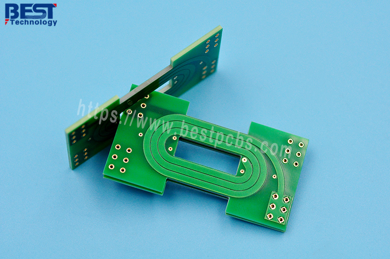
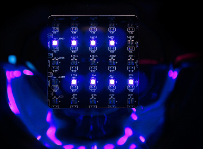
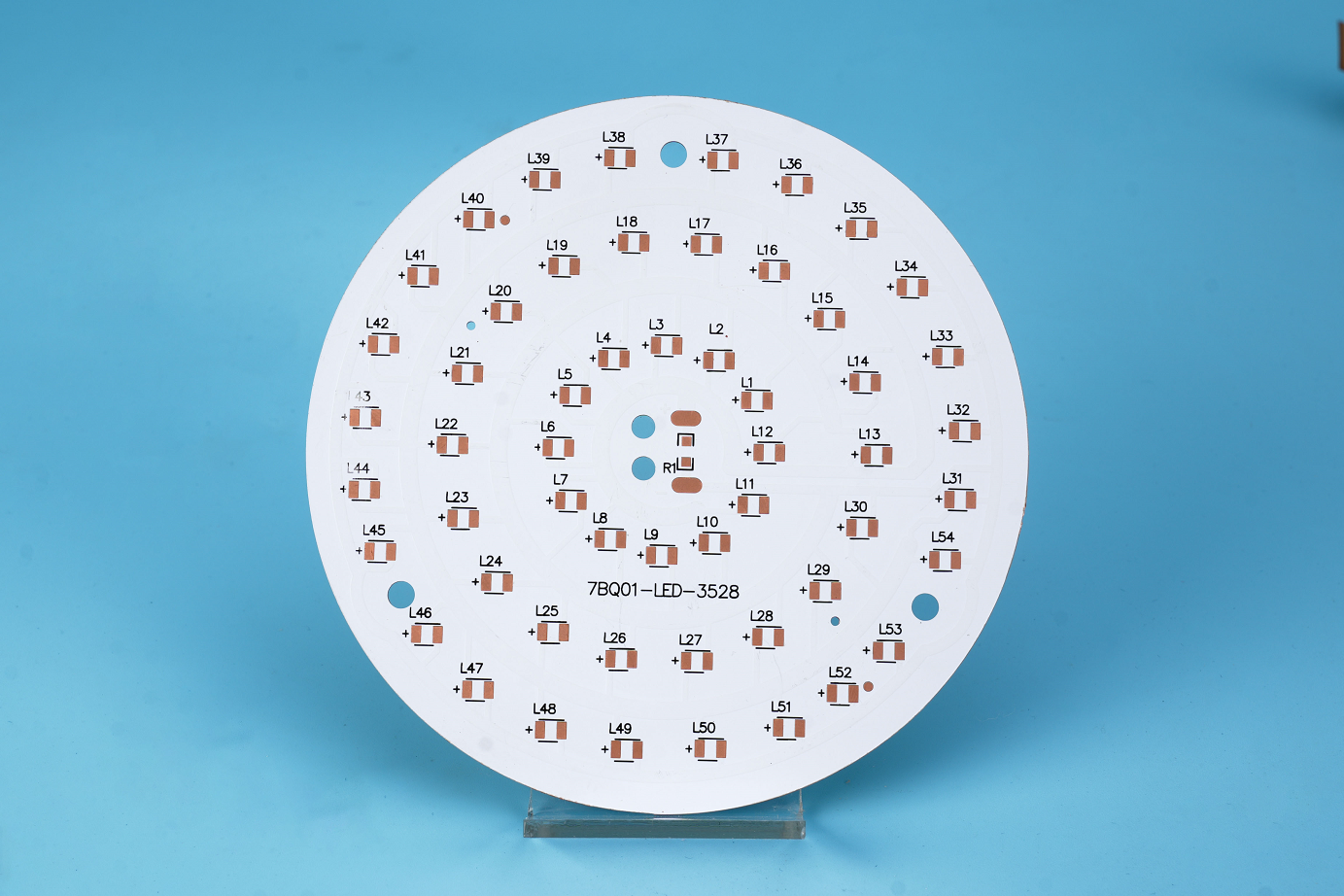
In the field of ultraviolet light-emitting diodes (UV LED), the integration of Metal Core Printed Circuit Boards (MCPCB) plays a significant role in improving UV LED performance, thermal management, and overall reliability. In this blog post, we will explore the importance of MCPCB in UV LED applications, highlighting its advantages with concrete data to demonstrate its practicality.

  1. Efficient Heat Dissipation:

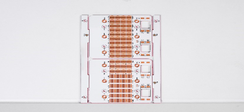
MCPCBs excel in efficient heat dissipation, ensuring optimal UV LED performance and longevity. With a metal core typically made of aluminum or copper, MCPCBs possess high thermal conductivity. For instance, MCPCBs have a thermal conductivity coefficient of normally 1.0-3.0 W/mK, it needs to be customized if the thermal conductivity exceeds 3.0W/mk. this exceptional thermal conductivity allows for rapid dissipation of generated heat, preventing heat accumulation and ensuring UV LEDs operate within their optimal temperature range.

2. Enhanced Thermal Conductivity:

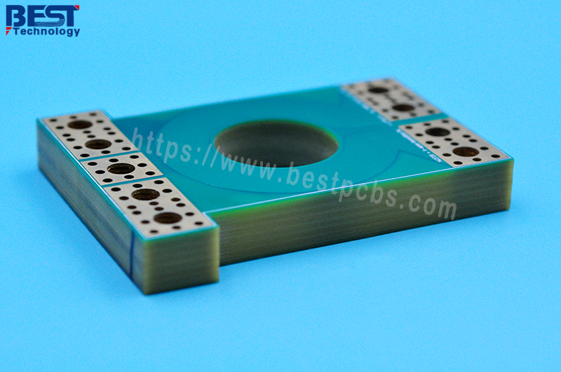
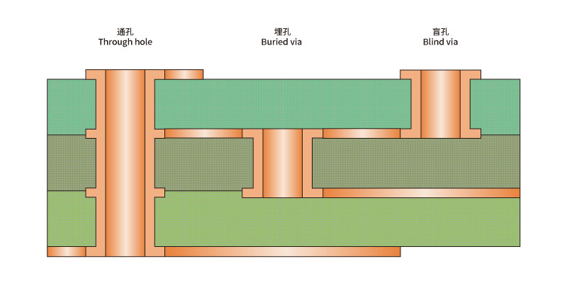
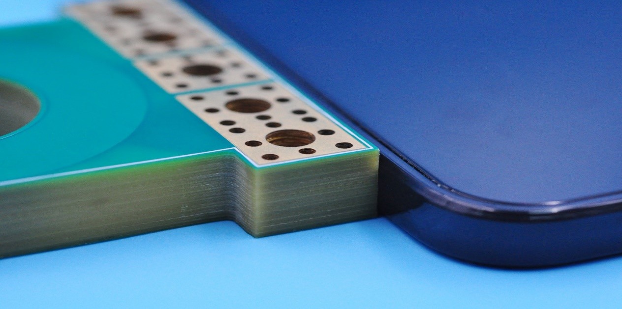
MCPCBs contribute to effective heat dissipation through improved thermal conductivity. Studies indicate that MCPCBs can enhance thermal conductivity up to ten times higher than standard FR4 PCBs. Because the stack up of MCPCB is different with PCB, please see below stack up. This enhanced thermal conductivity aids in achieving a uniform temperature distribution across the entire MCPCB, reducing the risks of hotspots and thermal stress on UV LEDs. Consequently, UV LEDs can maintain their performance and reliability even during extended operation.
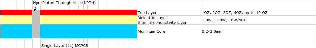
(MCPCB_stack_up)
1ozCopper layer
1.5mm without copperCore base
(FR4PCB_stack_up)

3. Reliability in Harsh Environments:

MCPCBs are designed to withstand harsh environments, ensuring reliability in UV LED applications. The metal core of MCPCBs provides higher mechanical strength and resistance to thermal stress. For example, the coefficient of thermal expansion (CTE) of an MCPCB can be matched with UV LEDs, minimizing the risk of mechanical failures caused by thermal mismatch. These features enable MCPCBs to operate reliably even in high-temperature environments or under exposure to ultraviolet radiation, thereby extending the lifespan of UV LED devices.

4. Electrical Isolation:

MCPCBs offer electrical isolation between the metal core and circuit layers, ensuring safe and reliable operation of UV LEDs. The dielectric layer, typically made of materials such as epoxy resin or thermally conductive dielectric (TCF), exhibits high breakdown voltage and insulation resistance. This electrical isolation minimizes the risk of short circuits or electrical interference, protecting UV LEDs and the entire system from potential damage.

5. Performance Optimization:

By incorporating MCPCBs into UV LED technology, manufacturers can optimize the performance of their UV LED devices. The improved heat dissipation and thermal conductivity of MCPCBs enable UV LEDs to operate at maximum efficiency. Research shows that using MCPCBs can reduce LED junction temperatures by up to 20-30°C, improving light output and enhancing overall performance. This optimal performance ensures consistent UV light generation, making MCPCBs an ideal choice for various UV LED applications, including curing, sterilization, and phototherapy.

Conclusion:

The use of MCPCBs in UV LED technology offers practical benefits in heat dissipation, thermal conductivity, reliability, and electrical isolation. Concrete data and research support the effectiveness of MCPCBs in efficient heat management, even in harsh environments, enabling reliable operation of UV LEDs. With enhanced performance provided by MCPCBs, UV LED systems can deliver consistent, efficient, and durable UV light output, expanding the possibilities of UV applications in various industries. The utilization of MCPCBs further solidifies their critical role as a key supporting technology in the UV LED field.

If you are designing a metal core PCB and seeking for a reliable manufacturer, welcome to leave you message or contact us directly.

Do You Know What Is HDI Board?

August 10th, 2023

HDI boards are a type of printed circuit board (PCB) technology that enables higher circuit density and smaller form factors compared to traditional PCBs. HDI boards are commonly used in applications where space is limited, such as mobile devices, wearables, and aerospace systems.

Best Technology has rich experience in HDI rigid flex pcb manufacturing, below is one of our 7 layers HDI rigid flex pcb.

In Best Technology, our HDI board usually has the blind holes or buried holes, and the minimum hole size usually is 0.1mm. This board has the blind and buried holes, and the minimum hole size is 0.1mm. 100 ohm differential impedance control with 50 single ended impedance control. It’s surface finish is ENIG, 1oz copper for outer layers, 1/2oz copper for inner layers, green solder mask with white silkscreen. total thickness is 1.4mm.

Here are some key features and aspects of HDI boards:

  1. High Density: HDI boards are designed to accommodate a large number of densely packed components and interconnections. They typically have multiple layers with high routing density, allowing for more complex circuitry in a smaller footprint.
  • Microvias: HDI boards extensively use microvias, which are very small holes drilled into the board to create electrical connections between different layers. Microvias are smaller in size compared to traditional vias, allowing for increased routing density.
  • Staggered and Stacked Microvias: HDI boards employ different types of microvias, including staggered and stacked microvias. Staggered microvias connect adjacent layers, while stacked microvias connect non-adjacent layers, providing even higher routing density.

Blind and Buried Vias: HDI boards often utilize blind and buried vias, which are vias that do not extend through the entire board. Blind vias connect an outer layer with one or more inner layers, while buried vias connect inner layers only. These vias help optimize space and increase routing capabilities.

  • Fine Pitch Components: HDI boards support the use of fine pitch components, such as microcontrollers, ball grid array (BGA) packages, and small surface-mount devices (SMDs). The high routing density and smaller features of HDI boards make them suitable for accommodating these tiny components.
  • Increased Signal Integrity: HDI boards can provide improved signal integrity due to shorter trace lengths and reduced noise interference. The compact design minimizes signal loss and impedance mismatches, allowing for better performance in high-frequency applications.
  • Design Considerations: Designing HDI boards requires expertise in factors such as layer stacking, via types, trace widths, and clearances. Advanced design software and manufacturing techniques are often employed to ensure precise alignment and reliability of the intricate interconnections.
  • Manufacturing Challenges: HDI boards can be more challenging to manufacture compared to standard PCBs. The use of smaller features and complex layer structures requires specialized fabrication techniques, such as laser drilling, sequential lamination, and precise registration control.

HDI technology has become increasingly prevalent in the electronics industry, enabling the development of smaller, lighter, and more sophisticated devices. It offers enhanced electrical performance, improved reliability, and greater design flexibility. If you have any comments about the HDI board, please feel free to contact Best Technology Team e-mail: sales@bestfpc.com.

Heavy Copper PCB for Industrial Power Supply

July 29th, 2023

All of us know the printed circuit board, but do you know what is the heavy copper PCB? Best Tech is a very experienced heavy copper PCB fabricator since year 2006. Heavy Copper PCB is a type of printed circuit board that features with thicker copper layers than standard FR4 PCBs. While conventional PCBs typically have copper thicknesses ranging from 1 to 3 ounces (per square foot), heavy copper PCBs have copper thicknesses exceeding 3 ounces and can go up to 20 or more ounces. These copper layers are typically found in the inner and outer layers of the PCB, heavy copper providing enhanced current-carrying capacity and improved heat dissipation capabilities.

The increased copper thickness in heavy copper PCBs allows them to handle higher currents without experiencing excessive heat buildup or voltage drops. This makes them well-suited for applications that require high power handling, such as industrial power supplies, power converters, motor drives, and automotive electronics. Heavy copper PCBs are designed to withstand harsh operating conditions and provide robust performance and reliability.

Today, we would like to talk about the heavy copper PCB used in Industrial Power Supply. In this blog post, we will explore the realm of Industrial Power Supply, delving into the design considerations, material selection, production challenges, exceptional heat dissipation, and unrivaled conductivity of Heavy Copper PCBs. Join us on this enthralling journey as we uncover the secrets behind their application in Industrial Power Supply scenarios, including the testing of inductance, capacitance, and resistance. Get ready to witness the power of Heavy Copper PCBs in the realm of Industrial Power Supply!

Firstly, before you are moving start for the design, it need to get to understand the Design guideline rules of heavy copper PCB.

From the guidelines of heavy copper PCB, it could get to know it encompass considerations such as trace width, trace spacing, and thermal relief patterns. The increased copper thickness necessitates wider traces to accommodate higher currents, while proper spacing is crucial to avoid thermal hotspots and ensure reliable operation. Additionally, selecting suitable materials with excellent mechanical strength and thermal properties is vital to ensure the robustness and longevity of Heavy Copper PCBs. Hope this will bring some ideas to you during your design.

Secondly, as a heavy cooper PCB manufacturing vendor, Best Tech would like to advise the Production Challenges for the heavy copper PCB.

During producing Heavy Copper PCBs presents manufacturers with a set of intricate challenges. Achieving uniform copper thickness across the board’s surface demands advanced plating techniques and precise control over process parameters. Careful attention must be given to the etching process to prevent over-etching, which can compromise the integrity of the copper layers. Moreover, the additional weight of copper requires a sturdy substrate to support the board’s structure. Manufacturers must navigate these challenges with expertise and precision to deliver high-quality Heavy Copper PCBs.

You may have a question in mind, why we need to use the heavy copper PCB for the Industrial Power Supply, because the heavy copper PCB have Exceptional Heat Dissipation and Conductivity: One of the standout features of Heavy Copper PCBs is their unrivaled heat dissipation capabilities. The increased copper thickness acts as a robust conductor, efficiently channeling heat away from power components. This exceptional heat dissipation prevents thermal stress and ensures the longevity and reliability of Industrial Power Supply systems. Additionally, the high conductivity of Heavy Copper PCBs enables efficient power transmission, reducing losses and improving overall system efficiency.

Furthermore, Heavy Copper PCBs undergo rigorous testing to ensure optimal performance in Industrial Power Supply applications. Inductance testing verifies the effectiveness of copper layers in reducing magnetic interference. Capacitance testing evaluates the ability of the PCB to store electrical energy, while resistance testing determines the conductivity and resistance of copper traces. These tests play a crucial role in validating the quality and performance of Heavy Copper PCBs in demanding power supply scenarios.

Heavy Copper PCBs find widespread applications in the field of Industrial Power Supply, particularly in the production of robust and efficient power control products. They are integral components in industrial power converters, motor drives, uninterruptible power supplies (UPS), and various automation systems. The exceptional heat dissipation and high current-carrying capacity of Heavy Copper PCBs make them ideal for handling the power demands of these applications, ensuring reliable and efficient power delivery.

Finally, in the world of Industrial Power Supply, Heavy Copper PCBs emerge as true powerhouses, combining meticulous design, advanced manufacturing processes, and exceptional heat dissipation capabilities. By adhering to design guidelines, overcoming production challenges, and conducting thorough testing, Heavy Copper PCBs prove their mettle in demanding power supply scenarios. As they continue to evolve, these powerhouses will shape the future of Industrial Power Supply, empowering systems with reliability, efficiency, and unrivaled performance. Prepare to witness the electrifying impact of Heavy Copper PCBs in the realm of Industrial Power Supply!

If you have more question heavy copper PCB for Industrial Power Supply, warmly welcomed to contact Best Tech for more get more information of heavy copper PCB which used in Industrial Power Supply. You can visit www.bestpcbs.com to know more about us.

Understanding Counterbore and Countersunk Holes in PCB Design

July 8th, 2023

When we talking about the holes in PCBs (Printed Circuit Boards), may somebody always curious about two special holes: Counterbore hole and Countersunk hole. They are easy to be confused and easy to misunderstanding if you are a layman of PCB. Today, we will introduce the differences between counterbore and countersunk for details, let’s keep reading!

What is a Counterbore Hole?

A counterbore hole is a cylindrical recess on a PCB that has a larger diameter at the top surface and a smaller diameter at the bottom. The purpose of a counterbore hole is to create space for a screw head or a bolt’s flange, allowing it to sit flush with or slightly below the PCB surface. The larger diameter at the top accommodates the head or flange, while the smaller diameter ensures that the fastener’s shaft or body fits snugly.

What is a Countersunk Hole?

On the other hand, a countersunk hole is a conical recess on a PCB that allows the head of a screw or bolt to sit flush with the PCB surface. The shape of a countersunk hole matches the profile of the fastener’s head, creating a seamless and level surface when the screw or bolt is fully inserted. Countersunk holes typically have an angled side, often 82 or 90 degrees, which determines the shape and size of the fastener head that will fit into the recess.

Counterbore VS Countersunk: Geometry

While both counterbore and countersunk holes serve the purpose of accommodating fasteners, their main difference lies in their geometry and the types of fasteners they accommodate.

Counterbore holes have a cylindrical recess with two different diameters, while countersunk holes have a conical recess with a single diameter.

Counterbore holes create a stepped or raised region on the PCB surface, whereas countersunk holes result in a flush or recessed surface.

Counterbore VS Countersunk: Fastener Types

Counterbore holes are primarily used for fasteners with a head or flange, such as bolts or screws that require a solid mounting surface.

Countersunk holes are designed for fasteners with a conical head, such as flathead screws or countersunk bolts, to achieve a flush surface.

Counterbore VS Countersunk: Drill angles

Different sizes and drilling angles of drill bits are offered for producing countersinks, depending on the intended use. These angles can include 120°, 110°, 100°, 90°, 82°, and 60°. However, the most frequently employed drilling angles for countersinking are 82° and 90°. For optimal outcomes, it is essential to align the countersink angle with the tapered angle on the underside of the fastener head. On the other hand, counterbore holes feature parallel sides and do not necessitate tapering.

Counterbore VS Countersunk: Applications

The choice between counterbore and countersunk holes depends on the specific requirements of the PCB design and the components being used.

Counterbore holes find applications in situations where a secure and flush fastening of components or mounting plates is necessary. They are commonly used to fasten connectors, brackets, or PCBs to an enclosure or chassis.

Countersunk holes are often employed when aesthetic considerations are important, as they provide a sleek and level surface. They are frequently used for mounting PCBs to surfaces where a flush finish is desired, such as in consumer electronics or decorative applications.

Counterbore and countersunk holes are important features in PCB design, enabling efficient component mounting and secure fastening. Understanding the differences between these two types of holes allows designers to select the appropriate option based on the specific requirements of their circuit board applications. Whether it’s ensuring a secure connection or achieving a visually pleasing finish, the choice between counterbore and countersunk holes plays a crucial role in the overall functionality and aesthetics of a PCB assembly.

Do You Know How Many Types of Holes in PCB

July 4th, 2023

In the vast realm of engineering and manufacturing, there exists a hidden world of holes, each with its own distinct purpose and position. These holes play a crucial role in facilitating various functions within mechanical and electronic systems. In this blog, we will embark on a journey to explore different types of holes in printed circuit board. So, fasten your seatbelts and let’s delve into the fascinating world of these essential engineering features.

Common Types of Holes in PCB

Upon examining a circuit board, one will discover an array of holes serving specific purposes. These include Via holes, PTH, NPTH, Blind holes, Buried holes, Counterbore holes, Countersunk holes, Location holes, and Fiducial holes. Each hole type fulfills a distinct role and function within the PCB, making it crucial to familiarize oneself with their characteristics to facilitate optimal PCB design.

1. Via holes

Via holes are small openings that connect different layers of a printed circuit board (PCB). They facilitate the seamless flow of signals and power between the layers, enabling efficient circuit design and transmission. Vias can be classified into two types: Plated Through-Holes (PTH) and Non-Plated Through-Holes (NPTH), each serving different functions.

2. PTH (Plated Through-Hole)

Plated Through-Holes (PTH) are vias with conductive material coating the inner walls. PTHs establish electrical connections between different layers of a PCB, allowing the passage of signals and power. They play a crucial role in interconnecting components, facilitating the flow of electrical current, and ensuring the functionality of the circuit.

3. NPTH (Non-Plated Through-Hole)

Non-Plated Through-Holes (NPTH) lack the conductive coating on their inner walls, making them suitable for mechanical purposes only. These holes are used for mechanical support, alignment, or as positioning guides, without establishing any electrical connections. NPTHs provide stability and precision, ensuring proper alignment of components within the circuit board. The mainly different between PTH and NPTH is the copper foil will be plated in the hole wall while NPTH no need to do plate.

4. Blind Holes

Blind holes are partially drilled holes that penetrate only one side of a circuit board. They are primarily employed to connect the outer layer of the board with the inner layer, enabling component mounting on one side while remaining hidden from the other. Blind holes offer versatility and help maximize space in complex circuit board designs.

5. Buried Holes

Buried holes are entirely enclosed within a circuit board, connecting inner layers without extending to the outer layers. These holes are hidden from both sides of the board and serve to establish connections and routes between inner layers. Buried holes allow for denser circuit board designs, reducing the complexity of routing traces and enhancing the overall functionality of the board. They provide a seamless and compact solution without any surface exposure.

6. Counterbore Holes

Counterbore holes are cylindrical recesses created to accommodate the heads of bolts, nuts, or screws. They provide a flat-bottomed cavity that allows the fasteners to sit flush or slightly below the surface of the material. The primary function of counterbore holes is to enhance the aesthetics and functionality of a design by providing a smooth and even appearance. These holes are commonly found in woodworking, metalworking, and engineering applications where a concealed or larger bearing surface is desired.

7. Countersunk Holes

Countersunk holes are conical recesses designed to house the angled heads of screws or fasteners. They are employed to ensure that the screw heads lie flush or slightly below the material surface. Countersunk holes serve both aesthetic and practical purposes, providing a sleek and flawless finish while reducing the risk of snags or protrusions. Their versatility makes them suitable for various applications, from furniture manufacturing to aerospace engineering.

8. Location Holes

Location Holes, also known as Reference Holes or Tooling Holes, serve as key reference points for aligning and positioning components, parts, or fixtures during manufacturing or assembly processes. These holes are strategically placed in a design to ensure precise and consistent alignment, enabling efficient assembly and reducing errors.

9. Fiducial Holes

Fiducial Holes, also referred to as Fiducial Marks or Alignment Marks, are small precision holes or markings placed on a surface or PCB (Printed Circuit Board). These holes serve as visual reference points for vision systems, automated processes, or machine vision cameras.

As we conclude our journey through the fascinating world of holes in engineering, we have gained a deeper understanding of the functions and positions of counterbore holes, countersunk holes, via holes, PTH, NPTH, blind holes, and buried holes. These holes are essential elements in various industries, contributing to the aesthetics, functionality, and efficiency of designs.

After introducing each of them, you should have gained a deeper understanding of their functions, hope this is helpful for you the design holes on your PCB project!!

Exploring the Possibilities of UV LED & Importance of MCPCB

June 12th, 2023

UV LED technology has opened up a world of possibilities in various industries, revolutionizing applications that require ultraviolet light. From curing adhesives to sterilizing water, UV LEDs have become indispensable in many fields. In this article, we will explore the possibilities of UV LED and discuss the crucial role that Metal Core Printed Circuit Boards (MCPCBs) play in enhancing its performance and reliability.

Introduction to UV LED

UV LED refers to light-emitting diodes that emit ultraviolet light in the range of 100 to 400 nanometers. Unlike traditional UV lamps, UV LEDs offer numerous advantages, including energy efficiency, compact size, and precise control over the emitted wavelength. These characteristics make UV LED technology highly versatile and suitable for a wide range of applications.

Where we can use UV LED?

UV LED lights are finding extensive applications in our daily life, below are some popular fields that it can be apply in.

  • Healthcare and Medicine

One promising area where UV LED lights are making a significant impact is in the field of disinfection and sterilization. UV-C radiation, emitted by UV LEDs, has been proven to effectively kill or inactivate microorganisms such as bacteria, viruses, and fungi. Unlike traditional disinfection methods, UV LED technology is safe, energy-efficient, and chemical-free. It finds applications in healthcare facilities, food processing, water purification, and air sterilization systems, ensuring a cleaner and healthier environment. Metal core PCB plays a crucial role in UV-C radiation since MCPCB has good durability and excellent corrosion resistance compared to traditional FR4 PCB. It makes the UV-C radiation performs high performances and long-time lifespan.

  • Industrial and Manufacturing

Another exciting application of UV LED lights is in advanced manufacturing processes, such as 3D printing and lithography. UV-curable resins and photopolymers can be rapidly cured using UV LED exposure, enabling faster production speeds and higher precision. Additionally, UV LED technology allows for the precise control of light wavelengths, which is crucial in fields like electronics, where specific wavelengths are required for the fabrication of microchips and displays.

  • Agriculture

UV LED lights are finding their way into horticulture and agriculture. UV-B radiation, emitted by UV LEDs, has been shown to stimulate plant growth, increase yields, and enhance crop quality. By tailoring the light spectrum using UV LEDs, growers can optimize plant development, promote flowering, and even modulate specific plant traits. The efficient heat dissipation of the metal core circuit board in UV-B radiation ensures prolonged functionality without concerns of excessive heat generated during extended operation. This technology has the potential to revolutionize indoor farming and enable year-round crop production in controlled environments.

  • Environmental Sustainability

UV LED lights play a vital role in environmental sustainability efforts. They are increasingly used for water and air purification systems. UV LED water purifiers effectively deactivate or destroy harmful microorganisms in water, providing safe drinking water without the use of chemicals. Additionally, UV LED air purifiers can eliminate airborne pathogens and allergens, improving indoor air quality. Metal core is a relatively environmentally friendly and healthy material, not only the material itself does not contain volatile substances such as benzene, but also through the solidification of ultraviolet light will form a dense curing film, which can reduce the release of harmful gases in the substrate. So metal core PCB as the substrate for UV LED is a good choice for demand of industry sustainable development.

Importance of MCPCB in UV LED Technology

With the big possibilities of the UV LED, the importance of MCPCB in UV LED technology cannot be overlooked. Thermal management is crucial for UV LEDs, as they generate a significant amount of heat during operation. Without proper heat dissipation, the performance and lifespan of UV LEDs can be compromised.

1. MCPCBs effectively address the thermal management challenges associated with UV LED technology. By efficiently dissipating heat, MCPCBs help prevent overheating, which can lead to reduced lifespan, color shifting, or even LED failure. The use of MCPCBs ensures that UV LEDs operate at their optimal temperature, maximizing their performance, and extending their lifespan.

2. Additionally, MCPCBs contribute to the overall efficiency of UV LED systems. By maintaining lower operating temperatures, MCPCBs minimize the energy losses due to heat. This improved efficiency translates into cost savings and a reduced environmental impact.

3. The last but not least, the reliable and stable construction of MCPCBs also contributes to the longevity and reliability of UV LED systems. With their excellent mechanical strength, MCPCBs protect UV LEDs from physical damage and ensure consistent performance over time.

As the demand for UV LED technology continues to grow, the importance of MCPCB in optimizing its performance and reliability will remain paramount. With ongoing advancements in MCPCB technology, we can expect even more efficient and durable UV LED systems in the future. Best Technology specializes in the manufacturing of MCPCBs. With our state-of-the-art factory and highly skilled engineering team, we can offer you the exceptional one-stop services. If you are currently engaged in a UV LED project and require a dependable supplier, we warmly invite you to reach out to us at your convenience. We are committed to providing reliable solutions for all your UV LED needs. Feel free to contact us anytime.

Exploring the Fascinating World of HDI PCBs

June 6th, 2023

In the ever-evolving realm of printed circuit boards (PCBs), High-Density Interconnect (HDI) technology stands out as a game-changer. HDI PCBs have revolutionized the electronics industry by enabling the creation of smaller, lighter, and more advanced electronic devices. In this blog, let us delve into the captivating world of HDI PCBs, exploring their unique processes and craftsmanship. We also attached some photos for your ref.

What is HDI PCB?

HDI PCBs, short for High-Density Interconnect PCBs, are a specialized type of circuit board designed to accommodate a higher number of components within a smaller footprint. Unlike traditional FR4 PCBs, HDI boards incorporate intricate designs and advanced manufacturing techniques to achieve denser routing and interconnections.

  • Miniaturization and Component Density

One of the standout features of HDI PCBs is their ability to achieve significant miniaturization. There are fine-pitch traces, microvias, blind and buried vias. You can see the below photo, there are many kinds of the vias.

HDI boards allow for more compact layouts and increased component density. This makes them ideal for applications where space is a premium, such as smartphones, tablets, wearables, and medical devices.

  • Advanced Manufacturing Techniques

Creating HDI PCBs involves a sophisticated blend of state-of-the-art manufacturing processes. These techniques include laser drilling, sequential lamination, and advanced imaging technologies. Laser drilling enables the creation of microvias, which are tiny holes used for interconnection between different layers of the board. Sequential lamination involves bonding multiple layers together, creating a compact stack-up with enhanced electrical performance. Advanced imaging technologies ensure precise alignment and accuracy during the fabrication process.

Benefits of HDI PCBs

HDI PCBs offer a multitude of advantages that make them highly sought after in today’s electronics industry:

1. Improved Signal Integrity: With their reduced parasitic effects and shorter signal paths, HDI boards provide superior signal integrity and enhanced electrical performance.

2. Increased Reliability: HDI PCBs minimize the risk of failures due to reduced interconnection lengths, better thermal management, and enhanced impedance control.

3. Enhanced Thermal Efficiency: The compact design of HDI boards allows for better heat dissipation and thermal management, ensuring optimal performance of heat-sensitive components.

4. Design Flexibility: HDI technology opens up new design possibilities, enabling engineers to create innovative and compact product designs without compromising on functionality.

Applications of HDI PCBs

The versatility of HDI PCBs makes them indispensable in various industries, including:

  • Consumer Electronics: Smartphones, tablets, laptops, and wearable devices.
  • Automotive Electronics: Advanced driver assistance systems (ADAS), infotainment systems, and autonomous driving technology.
  • Medical Devices: Miniature medical implants, diagnostic equipment, and patient monitoring systems.
  • Aerospace and Defense: Avionics, satellites, and military-grade electronics.
  • Industrial Automation: Robotics, control systems, and IoT devices.

We have many customers from various industries, the PCBs of the below photos are what we produced for our customers.

Conclusion

As technology advances, HDI PCBs will undoubtedly play a crucial role in driving innovation and pushing the boundaries of what is possible in the world of electronics.

We hope this exploration into the captivating world of HDI PCBs can make you know more about HDI PCB. If you’re interested in any HDI PCB, please feel free to contact us any time. Let us supply you an excellent solution and awesome boards for you.

What is UVLED? Is MCPCB important for UVLED?

June 3rd, 2023

UVLEDs, a subset of light-emitting diodes (LEDs), emit light within the ultraviolet spectrum instead of visible light like traditional LEDs. The UV spectrum is further divided into three main categories based on wavelength: UVA, UVB, and UVC. In this blog, we will explore the critical role of Metal Core Printed Circuit Board (MCPCB) in UVLED technology, highlighting its significance in improving efficiency, heat management, and overall lifespan.

UVA (315-400nm):

UVA, also known as near-ultraviolet, emits long-wave ultraviolet light. It is closest to the visible light spectrum and finds applications in UV curing, forensic analysis, counterfeit detection, tanning beds, and more.

UVB (280-315 nm):

UVB emits medium-wave ultraviolet light and is renowned for its biological effects. It is used in medical treatments, phototherapy, disinfection applications, and even for inducing vitamin D synthesis in the skin.

UVC (100-280 nm):

UVC emits short-wave ultraviolet light and possesses powerful germicidal properties. Its applications include water purification, air disinfection, surface sterilization, and eradication of bacteria, viruses, and other microorganisms.

UVLEDs typically operate within a temperature range of -40°C to 100°C (-40°F to 212°F). However, it is crucial to note that excessive heat can impact the performance, efficiency, and lifespan of UVLEDs. Therefore, appropriate thermal management techniques such as heat sinks, thermal pads, and adequate airflow are commonly employed to dissipate heat and keep UVLEDs within the optimal temperature range.

In conclusion, MCPCB plays a vital role in UVLED technology, offering essential advantages such as efficient heat dissipation, enhanced thermal conductivity, reliability in harsh environments, and electrical isolation. These qualities are paramount for maximizing UVLED performance, ensuring longevity, and maintaining optimal operating temperatures. The significance of MCPCB lies in its ability to enhance efficiency, improve heat management, and provide a reliable foundation for UVLED systems. Without MCPCB, UVLED applications would face challenges in heat dissipation, performance stability, and overall safety.

5 Tips Tell You How to Solder BGA Better in PCBA

May 29th, 2023

BGA (Ball Grid Array) soldering is a widely used method in the electronics manufacturing industry for mounting integrated circuits onto printed circuit boards (PCBs). This method provides a more compact and reliable connection compared to traditional through-hole or surface mount technology (SMT). However, the complexity of BGA soldering poses various obstacles during the manufacturing process. Herein, we will explore the challenges faced in BGA soldering and discuss effective strategies to address them.

What is BGA Soldering?

BGA soldering is a technique that involves the attachment of integrated circuit packages to a PCB using an array of solder balls. These solder balls are typically made of lead-based or lead-free alloys, depending on environmental regulations and specific requirements. The BGA package consists of a substrate, which acts as a carrier for the integrated circuit, and the solder balls that form the electrical and mechanical connections between the package and the PCB.

(BGA_balls)

The Importance of BGA Soldering in Electronics Manufacturing

BGA soldering plays a critical role in the manufacturing of various electronic devices such as computers, smartphones, and gaming consoles. The increased demand for smaller and more powerful electronics has driven the adoption of BGA packages. Their compact size and high pin density make them suitable for advanced applications where space is limited.

Challenges Faced in BGA Soldering

  • Component Alignment and Placement

One of the primary challenges in BGA soldering is ensuring accurate component alignment and placement on the PCB. The small size of the solder balls and the dense layout of the BGA package make it difficult to achieve precise positioning. Misalignment during the assembly process can result in solder bridges, open connections, or mechanical stress on the package.

To address this challenge, manufacturers employ advanced technologies such as Automated Optical Inspection (AOI) and X-ray Inspection. AOI systems use cameras and image processing algorithms to verify the correct alignment and placement of BGA components. X-ray inspection, on the other hand, allows manufacturers to see beneath the surface of the PCB and detect any misalignment or defects that may not be visible to the naked eye.

(Alignment)
  • Solder Paste Application

Another significant challenge in BGA soldering is achieving precise and consistent solder paste application. Solder paste, a mixture of solder alloy and flux, is applied to the PCB pads before placing the BGA package. Inadequate or excessive solder paste can lead to solder defects such as insufficient solder joints, solder voids, or solder bridging.

To overcome this challenge, careful attention must be given to stencil design and aperture selection. Stencils with appropriate thickness and properly sized apertures ensure accurate solder paste deposition. Additionally, manufacturers can employ Solder Paste Inspection (SPI) systems to verify the quality and consistency of the solder paste applied. The solder paste that Best Technology uses is SAC305 solder paste, which has good printability and excellent stability.

(SAC305_Solder_paste)
  • Temperature Profiling

Temperature profiling, or we can say the thermal management, it is crucial in BGA soldering to ensure proper reflow of the solder paste. The reflow process involves subjecting the PCB to a carefully controlled temperature profile, allowing the solder paste to melt, form a reliable joint, and solidify. Inadequate temperature profiling can lead to insufficient solder wetting, incomplete reflow, or thermal damage to components.

Manufacturers must optimize the reflow oven setup and calibration to achieve the correct temperature profile. Thermal profiling techniques, such as the use of thermocouples and data loggers, help monitor and control the temperature during the reflow process.

  • Reflow Process

The reflow process itself presents challenges in BGA soldering. The soak zone, ramp rates, and peak temperature must be carefully controlled to prevent thermal stress on the components and ensure proper solder reflow. Inadequate temperature control or improper ramp rates can result in solder defects such as tombstoning, component warpage, or voids in the solder joints.

Manufacturers need to consider the specific requirements of the BGA package and follow recommended reflow profiles provided by component suppliers. Proper cooling after reflow is also essential to prevent thermal shock and ensure the stability of the solder joints.

(BGA_reflow)
  • Inspection and Quality Control

Inspection and quality control are critical aspects of BGA soldering to ensure the reliability and performance of the solder joints. Automated Optical Inspection (AOI) systems and X-ray inspection are commonly used to detect defects such as misalignment, insufficient solder wetting, solder bridging, or voids in the solder joints.

(AOI)

In addition to visual inspection techniques, some manufacturers may perform cross-section analysis, where a sample solder joint is cut and examined under a microscope. This analysis provides valuable information about the quality of the solder joint, such as solder wetting, void formation, or the presence of intermetallic compounds.

In a word, BGA soldering presents unique challenges in electronics manufacturing, primarily related to various factors. By addressing these challenges effectively, manufacturers can ensure the reliability and performance of BGA solder joints, contributing to the production of high-quality electronic devices. Best Technology has rich experience in PCBA assembly and we mounted thousands PCBs for our customers, whatever it is simple design or complex design, all the products are assemble perfect and work well in customer side. Please feel free to contact us for any questions about PCBA.

Key Challenges in Solder Mask Printing for Heavy Copper PCBs

May 23rd, 2023

As the demand for higher power and miniaturization of electronics increases, so does the need for Heavy Copper Printed Circuit Boards (PCBs). From our last blog – Why choose Heavy Copper PCB for your High Current Project, we know the heavy copper PCBs are defined as those with copper thicknesses greater than 3 oz. These PCBs are designed to withstand high current and thermal loads, making them suitable for power electronics applications. However, the increased copper thickness also poses challenges during the solder mask printing process.

(16_layers_heavy_copper_PCB_with_10oz_each_layer)

Understanding solder mask

Solder mask (short for S/M in the industry) is a protective coating applied to PCBs to prevent solder bridges and improve solder joint quality. The solder mask is coated to the PCB surface using a screen-printing process, where the desired pattern is created using a stencil and the solder mask ink is then deposited onto the PCB. The ink is then cured, either through heat baking or UV light, to form a solid coating.

There are several types of solder mask materials available, including epoxy, acrylic, and liquid photo imageable (LPI) solder mask. Each type has its advantages and disadvantages, depending on the application requirements.

The benefits of using solder mask in PCB manufacturing include increased reliability, improved solderability, and reduced risk of short circuits and corrosion. The solder mask we usually use is Taiyo, which has high reliability and excellent heat resistance.

(Solder_mask_manually_printing)

Challenges in solder mask printing of heavy copper PCBs

While solder mask printing is a critical step in PCB manufacturing, the increased copper thickness in heavy copper PCBs presents several challenges for printing process as I mentioned before. It’s difficult to apply enough solder mask to cover thick copper pattern and base material with severe height difference.

1. The high copper thickness and thermal conductivity of heavy copper PCBs make it difficult for the solder mask ink to adhere properly to the surface. This can result in insufficient coverage and registration accuracy, which can affect the overall quality and reliability of the PCB.

2. The high copper thickness can cause stress on the solder mask, leading to mask cracking and peeling. The navigation mark on the substrate has specific ink thickness requirements due to limitations in the ink thickness that can be applied to the substrate. If the ink thickness on the substrate is too thick, it may result in solder resist cracks in the substrate position after the printed circuit board is soldered. This can occur during reflow soldering or thermal cycling, resulting in poor solder joint quality and reduced reliability.

3. The thick solder mask is also more difficult to exposure and develop. If the exposure energy is too weak or not enough, then some undercut problem may happen.

How to overcome this challenge?

To address these challenges, it is essential to choose the right solder mask materials and optimize the application process.

  • Choosing the right solder mask materials is crucial for ensuring proper adhesion and coverage on heavy copper PCBs. LPI solder mask is often preferred for heavy copper PCBs due to its excellent adhesion and thermal stability. However, epoxy and acrylic solder mask materials can also be used with proper surface preparation.
  • Optimizing the solder mask application process can also help address the challenges of heavy copper PCBs. This can include using a thinner stencil for improved registration accuracy and applying multiple coats of solder mask for better coverage. Advanced solder mask technology, such as laser direct imaging (LDI), can also help improve registration accuracy and reduce the risk of mask cracking and peeling.
  • Optimizing the printing process, now in Best Technology, we always make the substrate first, fill the substrate with the solder mask and then treat it as a normal PCB for normal printing solder mask.
(Solder_mask_printing)

If you are in the process of designing a complex multi-layer heavy copper PCB and are looking for a high-quality and experienced manufacturer, feel free to reach out to us at sales@bestpcbs.com, Best Technology can support you by OEM and ODM service to ensure your design is cost-effective and can be easily manufactured.