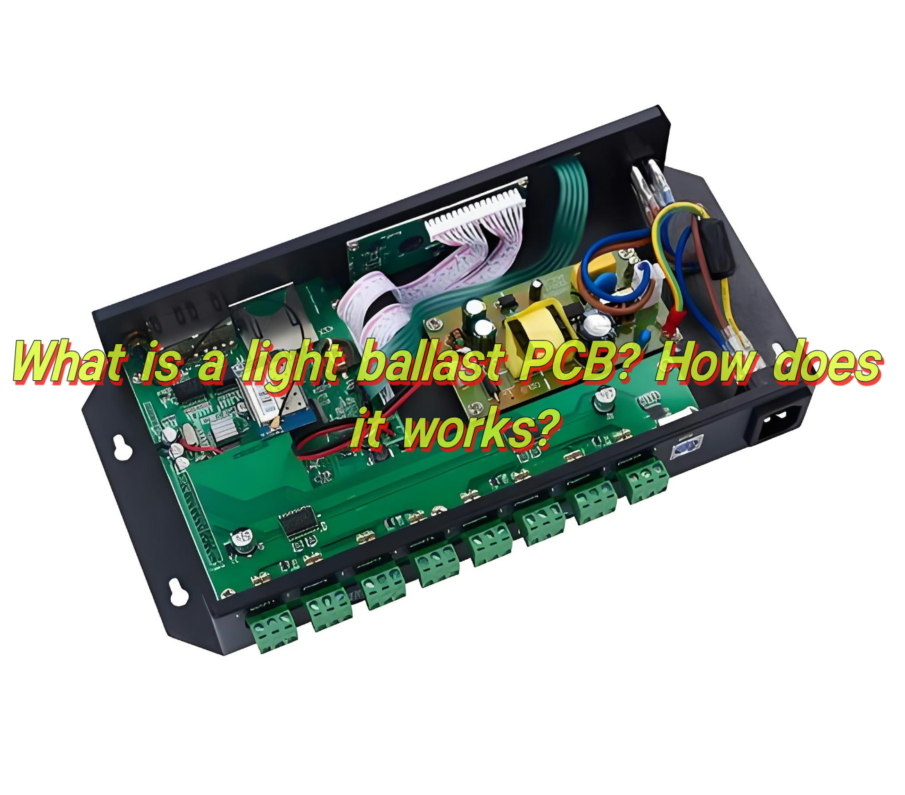
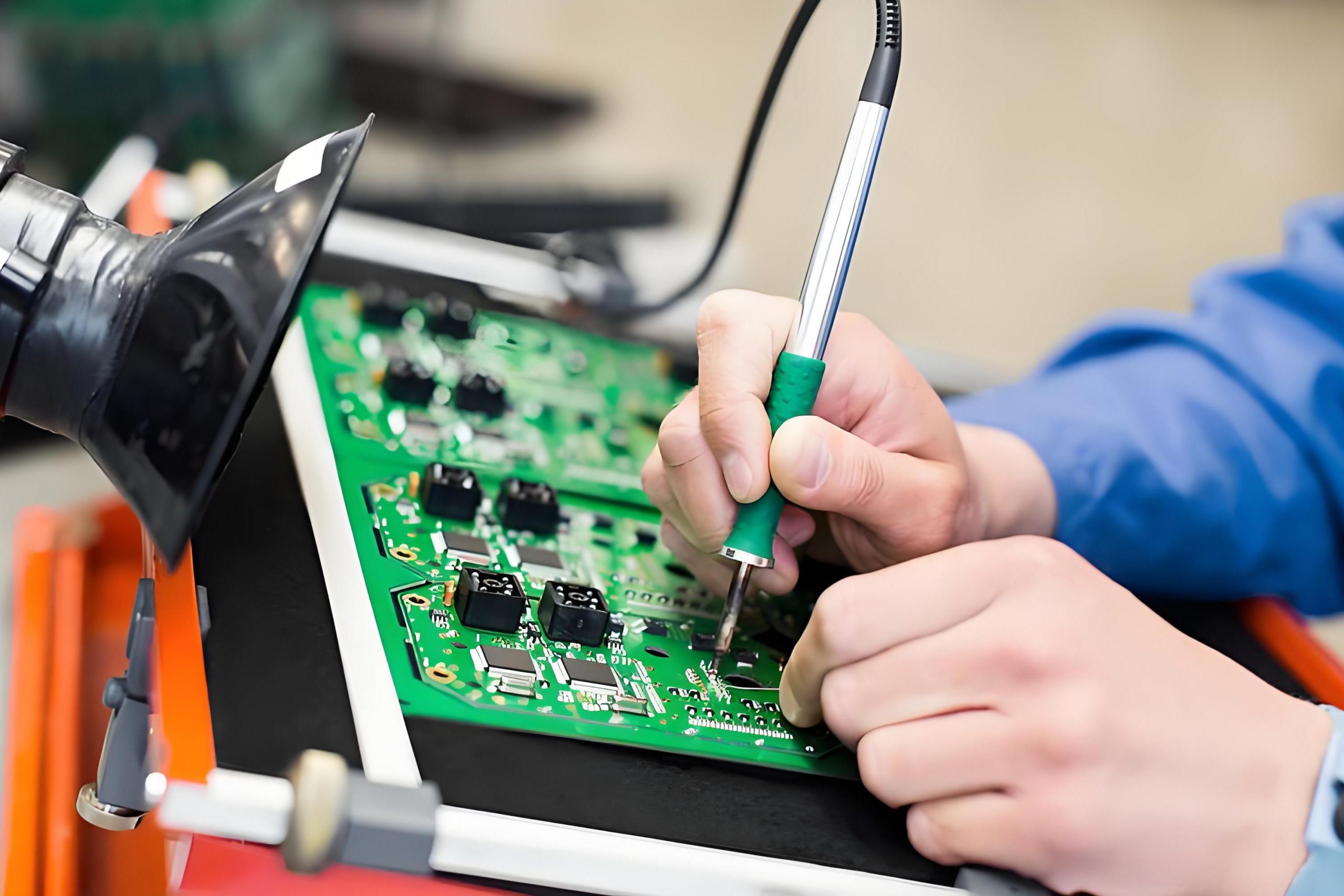
Metal Core PCB Heat Dissipation plays a key role in helping electronic devices handle rising temperatures during operation. For devices with power components, managing heat effectively can greatly impact performance, stability, and lifespan. A metal core PCB, often referred to as MCPCB, takes advantage of a metal layer to move heat quickly away from sensitive parts. This approach makes sure that devices stay cooler and more reliable, even in demanding conditions.
Now, let’s explore how these boards work, their unique traits, and why they stand out in thermal management.
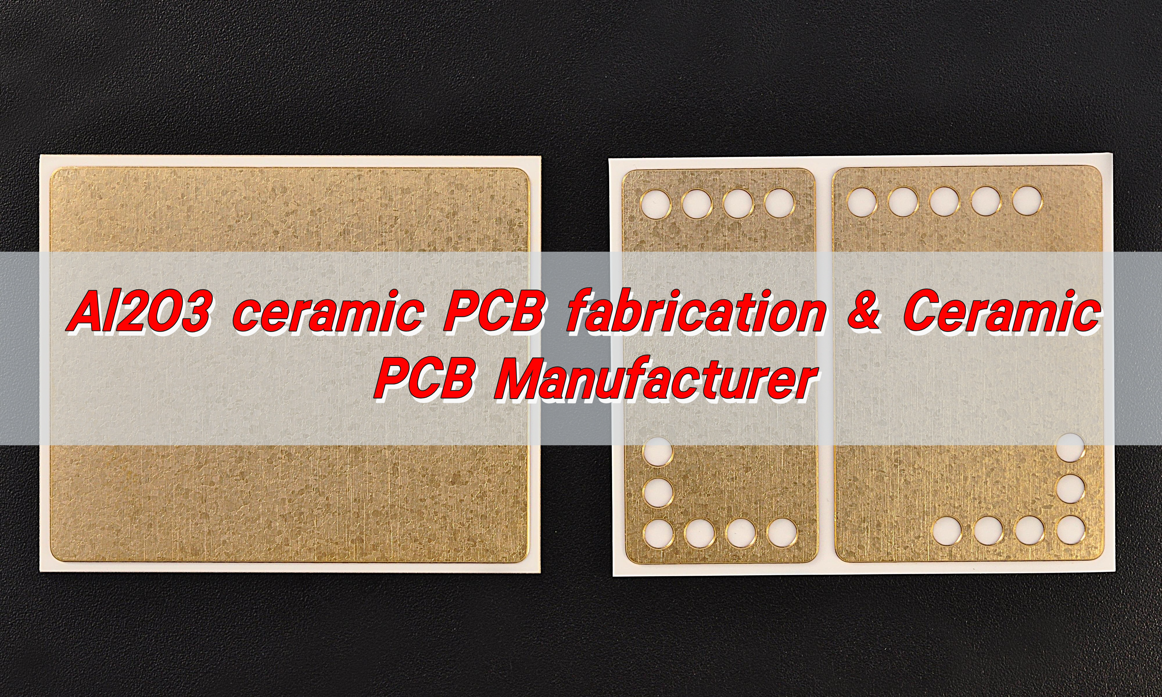
What is a metal core PCB?
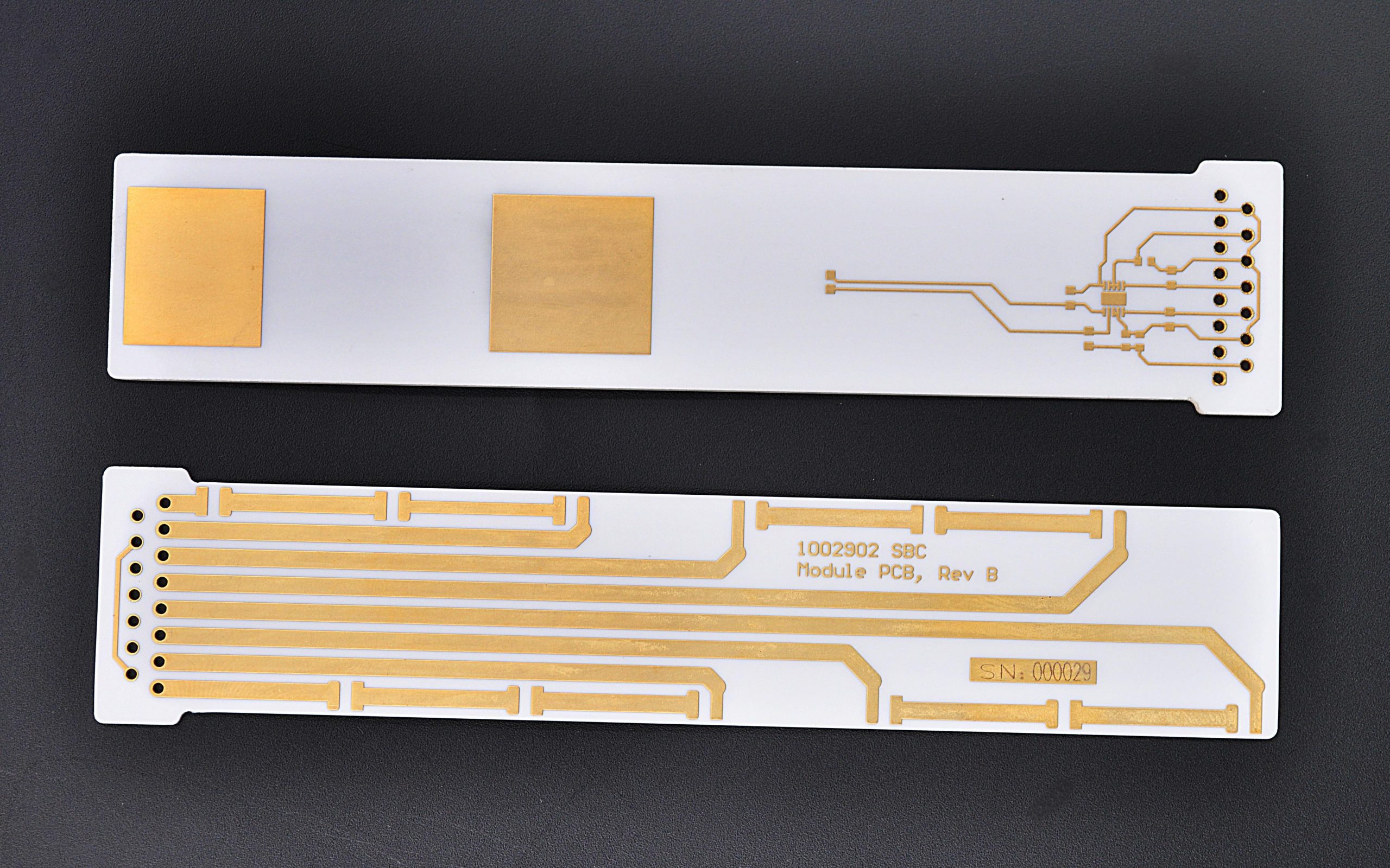
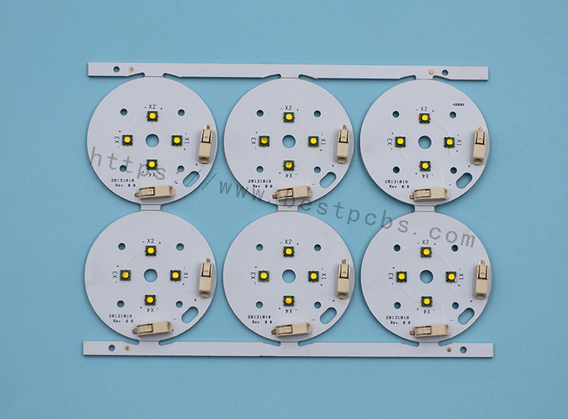
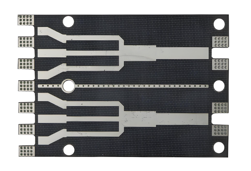
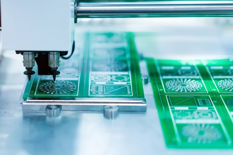
A metal core PCB uses a metal layer, typically aluminum or copper, as its base. This metal core replaces the usual fiberglass layer found in regular PCBs. The core helps with mechanical strength and, more importantly, heat transfer. How does a metal core PCB efficiently dissipate heat? Above the metal, you’ll find the dielectric layer and the copper traces for circuits. This design helps spread heat evenly across the surface, reducing hotspots.
Unlike traditional PCBs, which rely mainly on air or basic insulating materials for thermal relief, metal core PCBs offer a built-in solution for cooling. This structure makes them highly useful for high-power LED lighting, automotive electronics, and power supplies.
What is the difference between metal core PCB and FR4?
The biggest difference between metal core PCB and FR4 PCB comes down to the base material and thermal performance. FR4 boards use a glass-reinforced epoxy laminate, which is great for electrical insulation but poor at moving heat. Metal core PCBs, on the other hand, feature an aluminum or copper core that actively pulls heat away from hot components.
Because FR4 holds onto heat longer, it can struggle in high-power circuits, especially if components generate continuous heat. Metal core PCBs don’t just offer better thermal performance — they also support stronger structural integrity, especially in applications that face vibrations or physical stress.
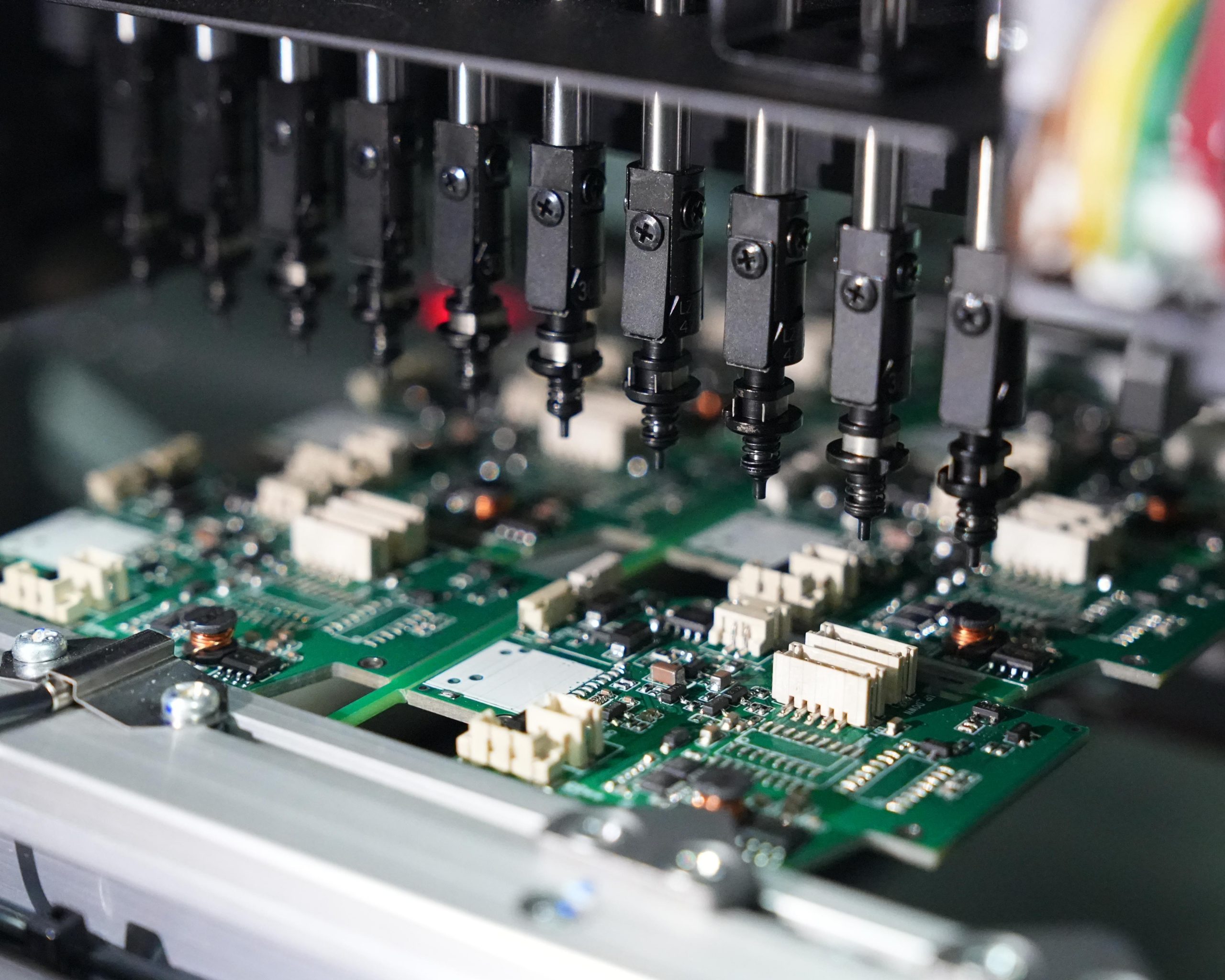
Another important difference relates to processing. Metal core PCBs need specialized drilling, cutting, and etching processes because of the hard metal layer, while FR4 can be handled with standard PCB manufacturing equipment.
What are the properties of metal core PCB?
Metal core PCBs stand out because of several beneficial properties that enhance both performance and durability. One key property is their superior thermal conductivity compared to traditional PCBs. This allows heat to flow smoothly from heat-generating components to the metal core, where it spreads and dissipates.
Another important property is mechanical strength. Metal cores provide strong support, which prevents the board from bending or warping under pressure. This stability helps in automotive, aerospace, and industrial environments where vibrations or impacts could damage weaker boards.
Additionally, these boards resist thermal expansion better than FR4. That means components stay more secure, even when exposed to wide temperature shifts.
Lastly, electrical insulation plays a vital role. Between the metal core and the copper layer, a special dielectric material separates conductive layers. This material balances heat transfer with high electrical resistance, keeping circuits safe from short circuits.
What is the thermal conductivity of a metal core PCB?
The Metal Core PCB Thermal Conductivity depends on the material used for the core and dielectric layer. Most aluminum core PCBs offer thermal conductivity between 1.0 to 2.5 W/mK for the dielectric layer. This may not sound high, but compared to FR4, which often measures around 0.3 W/mK, it’s a clear advantage.
The metal core itself — whether aluminum or copper — has a much higher thermal conductivity. Aluminum typically ranges around 200 W/mK, while copper exceeds 380 W/mK. This strong thermal performance helps the board remove heat faster than traditional options, keeping devices cooler for longer.
Thermal conductivity directly affects the speed at which heat spreads across the PCB, preventing localized overheating. This property makes metal core PCB heat dissipation so effective in demanding applications.
Is copper or aluminum better for heat dissipation?
Both copper and aluminum offer good thermal properties, but they excel in different areas. Copper has higher thermal conductivity, so it moves heat faster than aluminum. This makes it ideal for applications where thermal performance ranks above all else.
However, aluminum offers an excellent balance between cost, weight, and thermal efficiency. It performs well enough for most applications while keeping manufacturing costs lower. That’s why many LED lighting products, automotive controls, and consumer devices prefer aluminum core PCBs.
If weight is a concern, aluminum’s lower density helps create lighter boards, especially in handheld or mobile applications. For ultra-high power systems, copper may be the better option.
How fast does aluminum dissipate heat?
Aluminum stands out for its ability to spread heat quickly across its surface. Its thermal conductivity around 200 W/mK allows it to pull heat away from components almost immediately. This quick transfer reduces the chance of hotspots forming, which can extend component lifespan and improve stability.
Compared to many non-metallic materials, aluminum sometimes moves heat even up to 1000 times faster, making it especially valuable in Metal Core PCB Heat Dissipation applications. This fast heat dissipation supports efficient thermal management in LED lights, power amplifiers, and automotive controls.
What are the advantages of metal core PCB?
One clear advantage of metal core PCB technology lies in its exceptional heat management. By transferring heat directly into the metal core, these boards keep components cooler without needing external heat sinks in many cases.
Another key advantage comes from structural stability. The metal core adds rigidity, so the PCB resists bending or cracking, even under mechanical stress.
These boards also handle thermal cycling better than traditional materials, reducing the risk of cracks forming around solder joints. This helps in applications with frequent temperature swings, like outdoor lighting or automotive electronics.
Besides thermal and mechanical benefits, metal core PCBs offer better EMI shielding, especially when using a copper core. This can reduce electromagnetic interference, which helps improve signal integrity in sensitive circuits.
Finally, cost-efficiency in certain high-power applications means you may not need separate heat sinks or thermal pastes, saving on assembly costs.
What are the applications of metal core PCB?
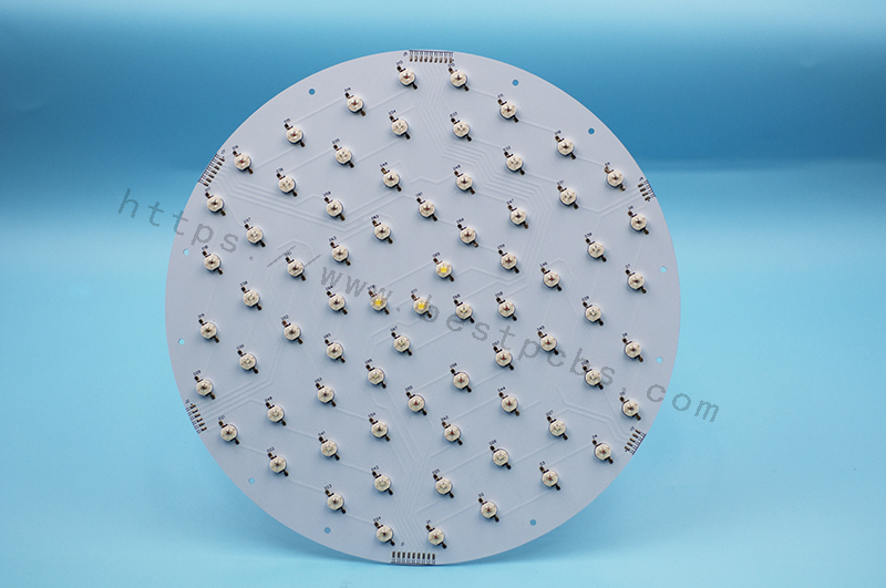
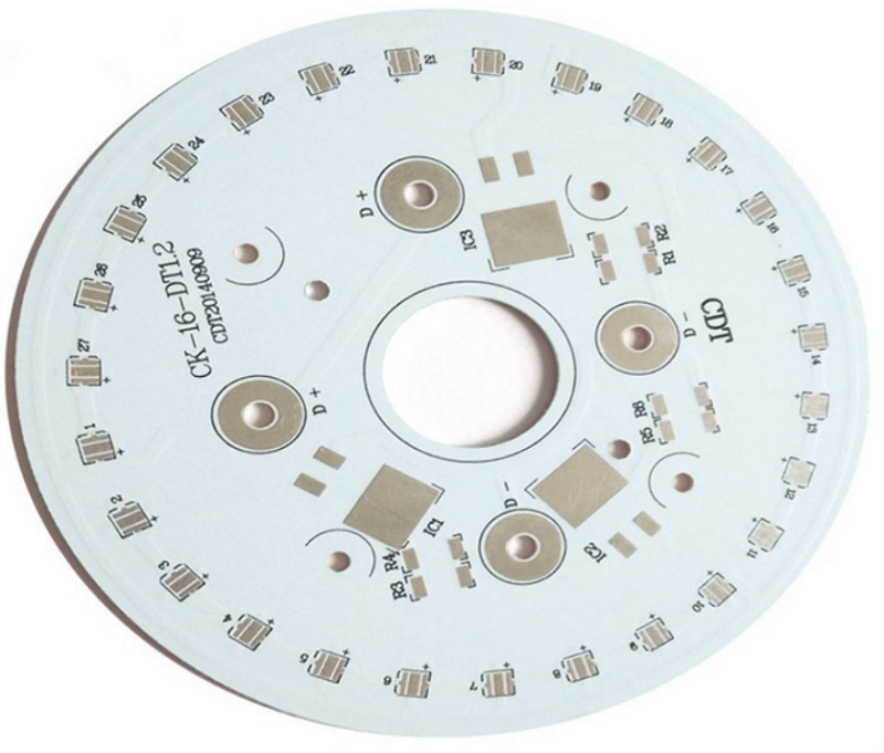
Metal core PCBs have found success in a wide range of applications where efficient heat management matters most. LED lighting products, especially high-power fixtures, often rely on these boards to keep LEDs running cooler for longer.
In automotive electronics, where heat from engines and power systems can cause issues, metal core PCBs help maintain stable performance even in harsh conditions.
Power supplies, particularly high-current converters and amplifiers, also benefit from the thermal and structural properties of metal core boards. These boards help maintain reliable operation by spreading heat away from heat-generating components.
Other industries, including renewable energy, industrial equipment, and military electronics, all benefit from the reliable heat dissipation and mechanical strength these boards provide. Anywhere heat buildup threatens performance or reliability, metal core PCBs offer a clear solution.
In conclusion, when it comes to managing heat in modern electronics, metal core PCB heat dissipation stands out as one of the most effective methods available. By transferring heat away from components into a metal core, these boards improve stability, extend lifespan, and support higher power densities than traditional PCBs.
If your product demands high reliability in a thermally challenging environment, choosing a trusted metal core PCB supplier can make a noticeable difference. At Best Technology, we combine 19 years of manufacturing experience with advanced materials and precise processing techniques to deliver metal core PCBs suited for demanding applications.
With custom design support, high-quality materials, and competitive pricing, we help businesses achieve better performance while keeping costs under control. Contact our team at sales@bestpcbs.com for more details.