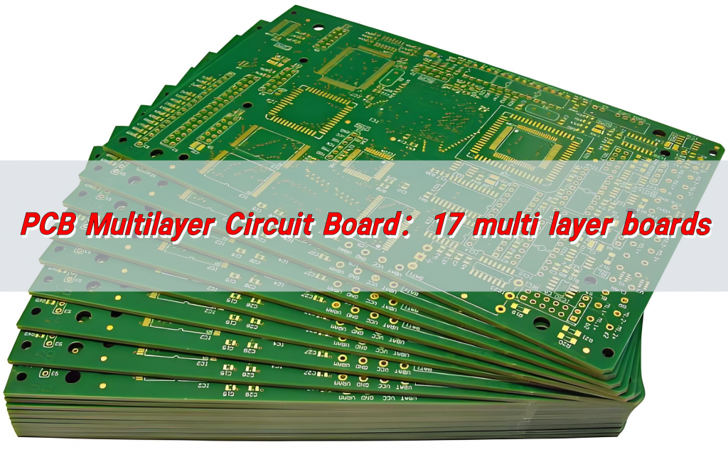
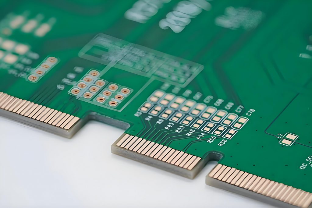
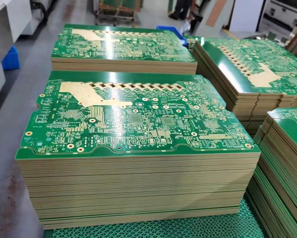
The 17 multi layer boards is a highly integrated electronic component that alternately stacks 17 conductive layers and insulating layers and uses advanced interlayer connection technology (such as vias) to achieve electrical connection between the layers. Connections can significantly increase the wiring density and complexity of circuits. This design makes the 17 multi layer boards has broad application prospects in high-performance electronic equipment and can meet the strict requirements of these equipments for signal transmission speed, stability and functional diversity.
What is a multi-layer circuit board?
The basic structure of a multilayer circuit board includes multiple conductive layers and insulating layers. The conductive layer usually uses copper foil or metallized holes, and the insulating layer is usually made of materials such as epoxy resin. Each layer is electrically connected through via holes, which are usually processed by drilling, laser drilling or chemical etching.
Advantages of multilayer circuit boards
- High wiring density: Multi-layer circuit boards can achieve more complex wiring in a limited space to meet the needs of high-density electronic equipment.
- Good electromagnetic shielding effect: The multi-layer design can effectively reduce electromagnetic interference and improve the stability and reliability of the system.
- Low signal transmission delay: Multi-layer circuit boards reduce signal transmission delay and improve system performance by optimizing wiring and signal paths.
- Suitable for complex systems: Multi-layer circuit boards are suitable for electronic devices that require a high degree of integration and complex functions, such as smartphones, tablets, etc.
How to make 17 multi layer boards?
The detailed steps for manufacturing a 17 multi layer boards are as follows:
- Raw material preparation: Choose high-quality copper-clad laminates as raw materials. Commonly used copper-clad laminates include epoxy glass cloth substrates, etc.
- Cutting: Use an automatic cutting machine to cut large-sized copper clad laminates into specific substrate sizes suitable for production needs.
- Drilling: Use a CNC drilling machine to accurately drill holes at predetermined positions on the copper clad board.
- Copper deposition: Copper ions in the electrolyte are deposited on the hole walls through electrochemical methods to form a uniform copper foil layer.
- Dry film exposure and development: Use dry film for exposure and development, and use strong ultraviolet light to polymerize the dry film to form a preliminary cured circuit pattern.
- Electroplating: In the electroplating production line, a layer of copper is plated on the exposed lines and hole walls through electrochemical reaction, and then a layer of tin is plated on the surface of the copper layer to protect the copper foil of the lines and hole walls from being eroded by the etching liquid.
- Stripping and etching: Place the PCB in the stripping equipment, use stripping agent and cleaning methods to remove the remaining dry film, exposing the copper foil that is not protected by tin plating. Then use an etching solution to etch away the exposed copper foil, retaining the copper foil under the tin plating layer, and finally obtain the circuit pattern and metallized holes required for the design.
- Inner layer process: Compared with single and double panels, the manufacturing of multi-layer boards has an additional inner layer process. Controlling the lamination process of the inner layers is critical to the electrical performance of controlled impedance transmission lines. The copper in the inner layer should be evenly distributed on the symmetrical layer to ensure balanced thermal stress during heating and avoid circuit board warping.
- Laminated lamination: By combining different specifications of prepreg and copper-clad laminate (core board), all required thicknesses are achieved. The individual layers must be symmetrical and have the same layer thickness. After the lamination is completed, precise inter-layer adjustment and positioning are performed to ensure good adhesion between the inner layer and the prepreg.
- Inspection: Circuit graphics are inspected using an automated optical inspection (AOI) system to ensure consistency of internal layers with CAD data and repair any connections or other defects found.
Through the above steps, a high-quality 17 multi layer boards can be manufactured.
When to use 17 multi layer boards?
1. High-frequency and high-speed signal processing scenarios
In communication base station equipment, such as the baseband processing unit (BBU) of a 5G base station. 5G signals have high frequency, large bandwidth, and extremely fast signal transmission speed. The 17 multi layer boards can efficiently route high-frequency, high-speed signals.
It can make the distance between the signal layer and the reference plane (ground layer) closer by reasonably arranging the positions of the signal layer, ground layer, and power layer, thereby reducing the loop inductance of the signal and reducing signal reflection and attenuation.
And some inner shielding layers can be used to isolate signals in different frequency bands or sensitive signals from interference sources to ensure the integrity and accuracy of signal transmission.
For the communication line between the graphics processing unit (GPU) and the central processing unit (CPU) in high-speed computer systems. When performing large-scale graphics rendering or complex data operations, the data transfer rate is extremely high.
The 17 multi layer boards can provide enough wiring space to route high-speed differential signal pairs (such as PCI-Express interface signals) on different inner layers. At the same time, a complete ground plane is set up around it as a shield to reduce electromagnetic interference and ensure high speed. signal quality.
2. Complex circuit function integration
In the electronic control part of advanced medical equipment such as magnetic resonance imaging (MRI) equipment. MRI equipment contains complex radio frequency transmitting and receiving circuits, gradient magnetic field control circuits, image acquisition and processing circuits and other functional circuits. The 17 multi layer boards can distribute these circuits with different functions on different layers and connect them through vias.
In the controller of industrial robots, it needs to integrate multiple functions such as motion control, sensor signal processing, communication interfaces, and power management. The 17 multi layer boards allows the circuits of these functional modules to be reasonably distributed on each layer, making the layout of the circuit board more compact.
3. Special power and grounding requirements
In high-precision test and measurement instruments, such as spectrum analyzers. This type of instrument has extremely high requirements on the purity and stability of the power supply. The 17 multi layer boards can be equipped with multiple independent power layers, and decoupling capacitors are reasonably arranged between the power layer and the ground layer to form a low-pass filter network to effectively filter out power supply noise.
At the same time, through reasonable ground layer design, low-impedance ground paths are provided for different circuit modules to reduce the impact of ground bounce noise on measurement accuracy.
Active power filters (APF) in power electronic equipment. APF needs to process a large number of power signals and plays a key role in improving power quality. The 17 multi layer boards can provide suitable power and ground planes for different power conversion circuits and control circuits.
What are the disadvantages of 17 multi layer boards?
The disadvantages of 17 multi layer boards mainly include the following aspects:
- 1. High cost: Due to the large number of layers and the complex manufacturing process, which requires more materials and finer processes, the cost is relatively high.
- 2. Design is difficult: Designing a 17-layer PCB requires more factors to be considered, such as inter-layer connections, signal integrity and electromagnetic compatibility, etc. This requires higher professional skills from the designer and the design cycle may also be longer.
- 3. Long production cycle: The production of multi-layer PCB involves multiple processes, such as lamination, drilling, copper plating, etc. These processes take time to complete, so the production cycle is relatively long.
- 4. Difficulty in maintenance: Due to the complex internal structure, once a fault occurs, it is relatively difficult to locate and repair the problem, and sometimes even requires complete replacement.
- 5. High requirements for design and manufacturing processes: more advanced equipment and technology are needed to ensure the quality and performance of multi-layer boards.
These shortcomings make 17 multi layer boards a reasonable trade-off between performance and cost in some applications.
How many layers can a circuit board have?
The number of layers in a circuit board can vary from single layer to multiple layers. Common layers include single layer, double layer, four layer, six layer, eight layer, ten layer, etc. High-end PCB boards can even reach 32 layers or more.
Application scenarios for different layers
- Single-layer board: Suitable for simple circuit design, usually used in low-complexity electronic devices.
- Double-layer boards: Suitable for medium-complexity designs that can accommodate more components and connections.
- Four-layer board: Commonly used in designs that require better signal isolation and noise suppression, such as high-frequency circuits.
The manufacturing process of multilayer boards is very complex and requires more precise design and high-end processing technology. The more layers there are, the higher the manufacturing difficulty and cost. Therefore, when designing a circuit board, it is necessary to consider the circuit direction, number of layers, and materials to ensure the performance and reliability of the circuit board.
How many layers of circuit boards can we make?
With the continuous advancement of electronic technology, we are able to produce PCBs with more layers. Currently, FR4 PCBs with 20 to 32 layers can be realized. This high-level PCB structure provides engineers with greater design flexibility, allowing them to lay out various traces on different layers to meet different functional requirements.
Layers can be dedicated for power distribution, signal transmission, electromagnetic interference (EMI) shielding, and assembly of components. In order to effectively manage the number of layers, buried holes and blind holes are often designed in multi-layer PCBs to optimize circuit layout and signal transmission paths.
For PCBs with more than 8 layers, high Tg FR4 materials are usually more popular than ordinary Tg FR4 because high Tg materials can maintain stable electrical performance and mechanical strength at higher temperatures, which is especially important for high-performance electronic devices. However, the increase in the number of layers also makes the PCB manufacturing process more complex and difficult, leading to higher costs.
In summary, we found that the 17 multi layer boards has significant advantages in signal integrity and space utilization, and can meet the needs of high-density electronic equipment, but its complex manufacturing process also brings higher costs and Production difficulty.
As a professional PCB manufacturer, BEST Technology has advanced production equipment and rich production experience, able to efficiently produce high-quality multi-layer PCB boards to meet customer needs for high-performance electronic equipment. Please feel free to contact us at sales@bestpcbs.com, we will provide a full range of services from design to production to ensure that every PCB board meets your strict standards.


