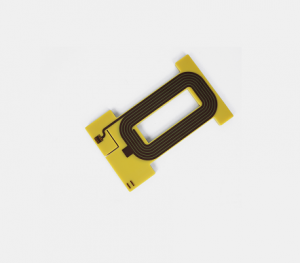
What is a 4 Layer PCB?
A 4 layer PCB is a type of circuit board that consists of four distinct layers of conductive material. Each layer serves a specific function. The layers typically include two signal layers, one ground (GND) layer, and one power (VCC) layer. Generally, through holes, buried holes, and blind holes are used to connect the internal layers. There are more buried and blind holes than 2 layer PCB boards. In addition, try not to run signal track on the two layers of VCC and GND. A 4 layer PCB offers more complex designs, better signal integrity compared to simpler designs.

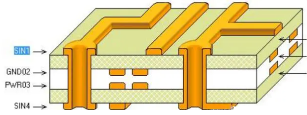
4 Layer PCB Stack-up
The typical stack-up configuration is as follows:
- Top Layer (Signal Layer): This layer carries signals and connections.
- Inner Layer 1 (Ground Plane): This layer serves as a reference for signal return paths, reducing noise and interference.
- Inner Layer 2 (Power Plane): This layer distributes power to various components on the PCB.
- Bottom Layer (Signal Layer): Like the top layer, it carries additional signals and connections.
4 layer PCB Stack up Options
Generally, there are three main categories for preferred stack-up solutions for 4 layer PCBs:
Solution 1: The standard layer setup for common 4 layer PCBs.
TOP (signal layer)
GND1 (ground layer)
PWR1 (power layer)
BOT (signal layer)
Solution 2: Suitable for situations where key components are laid out on the BOTTOM
layer or key signals are routed on the bottom layer; generally applicable under certain restrictions.
TOP (signal layer)
PWR1 (power layer)
GND1 (ground layer)
BOT (signal layer)
Solution 3: Suitable for PCBs primarily using through-hole components, commonly
used where the power is routed in layer S2, and the BOTTOM layer serves as a ground plane, thereby forming a shielding cavity.
GND1 (ground layer)
S1 (signal layer)
S2 (signal layer)
PWR1 (power layer)
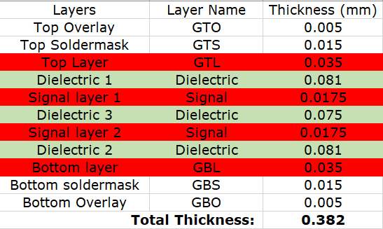
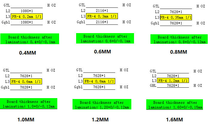
4 Layer PCB Thickness
The thickness of a 4 layer PCB can vary depending on the design requirements. Generally, a standard 4 layer PCB thickness ranges from 0.4mm to 1.6mm. The total thickness is determined by the materials used and the copper weight on each layer. A thicker PCB can offer better thermal management and mechanical stability, making it suitable for high-power applications. Here are the 4 layer PCB thickness with different thickness in Best Technology:
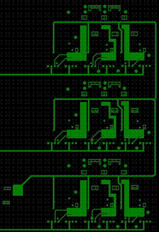
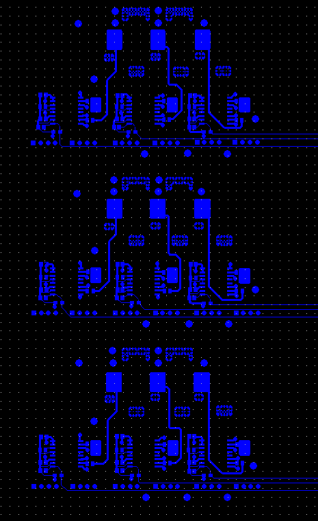
4 Layer PCB Manufacturing Process
Cutting material and grinding → drilling positioning holes → inner layer circuit → inner layer etching → inspection → black oxide → lamination → drilling → electroless copper → outer layer circuit → tin plating, etching tin removal → secondary drilling → inspection →print solder mask→Gold-plated→Hot air leveling→print silkscreen→routing outline→Test→Inspection
Ground Plane Design in 4 Layer PCB
The ground plane in a 4 layer PCB is essential to ensuring good performance and signal integrity. Here’s how to design an effective ground plane:
1. Purpose of the Ground Plane
- Reference Point: It provides a stable reference for signals, reducing noise and improving signal integrity.
- Return Path: It acts as a low-resistance return path for signals, minimizing electromagnetic interference (EMI).
2. Placement in Stack-up
Typically, the ground plane is placed as one of the inner layers, often Inner Layer 1. This positioning helps shield signals on the top and bottom layers.
3. Continuous Ground Plane
Aim for a solid, uninterrupted ground plane. Breaks or cuts can introduce impedance and increase noise.
4. Vias and Connections
- Use vias to connect components to the ground plane. Ensure that vias are placed close to component pads to minimize inductance.
- Consider using multiple vias for high-current paths to distribute the current effectively.
5. Thermal and Electrical Considerations
Use thermal vias if heat dissipation is a concern. Place them near high-power components to spread heat away from sensitive areas. Ensure that the ground plane is thick enough to handle the expected current loads without excessive voltage drop.
6. Control EMI
- Keep the ground plane as large as possible to effectively shield signals from external interference.
- Route high-speed signals away from ground plane edges to minimize crosstalk.
7. Simulation and Testing
- Use simulation tools to analyze the ground plane’s performance. Check for potential issues such as ground loops or noise.
- After fabrication, test the PCB to ensure that the ground plane functions as intended, with minimal interference.
What is the Advantage of a 4 Layer PCB Over a 2 Layer PCB?
While 2-layer PCB boards have their advantages, multi-layer designs are more beneficial for some applications. Today Best Technology will introduce the difference between 2-layer PCB board and 4 layer PCB.
1. A 4 layer PCB has an inner layer, which is laminated with PP and copper foil on both sides during the lamination process. This is pressed under high temperature and high pressure to form a multilayer board. Some circuits on the PCB 4 layer board are etched through the inner layer and pressed; the 2 layer PCB can be directly cut and drilled after production.
2. The 4 layer PCB is made of four layers of fiberglass, which can reduce the cost of the PCB, but the production efficiency is lower than that of the 2 layer PCB.
3. It is difficult for most people to distinguish a 4 layer PCB by observing the cross-section of the circuit board, but it can be identified by looking at the vias. If the same vias can be found on both sides of the PCB, or if the motherboard or graphics card is facing a light source and the vias do not allow light to pass through, then it is a 4 layer PCB.
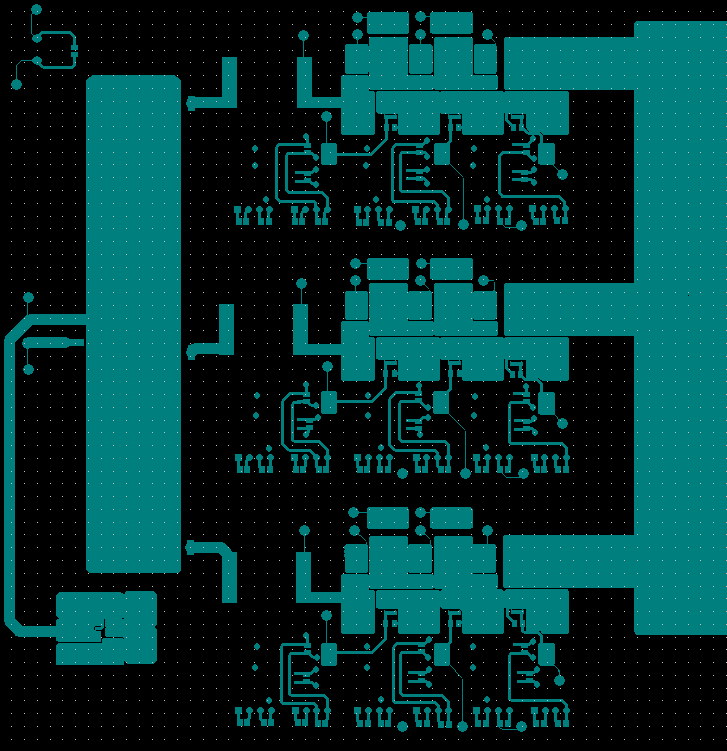
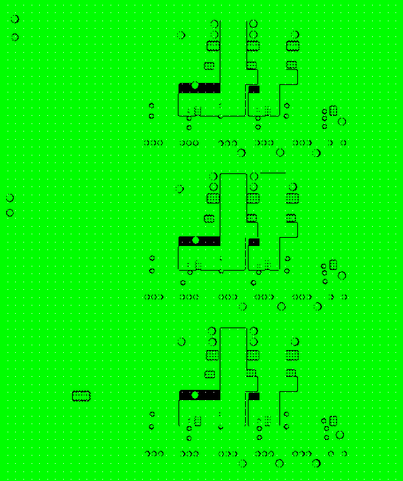
4. The PCB 4 layer board has dense routing, with the top layer being the front and the bottom layer being the back.
5. The PCB 4 layer board can distribute wiring among multiple layers, which increases design flexibility and allows better control of differential impedance, single-ended impedance, and improved output for certain signal frequencies.
How to Design a 4 Layer PCB?
When designing a 4 layer PCB, it is important to differentiate between the power layer and the signal layer. The signal layer is a positive output, while the power layer is a negative output. This means that lines drawn on the signal layer will result in actual copper traces, whereas lines drawn on the power layer indicate the removal of copper. Essentially, drawing lines on the power layer corresponds to removing copper, while drawing lines on the signal layer represents creating copper traces. Therefore, when designing the power layer, you can use lines to divide the copper area into separate regions, which is known as “power segmentation.” Here is a simple design step of a 4 layer PCB:
1. Schematic Design and Drawing
2. After completing the schematic drawing, import it into the PCB software, and complete the layout with a simple arrangement.
3. Follow the plan to design the stack-up, paying attention to the following aspects:
- You can generate multilayer PCB stack-ups yourself, with the default being two layers.
- Choose the unit of measurement.
- Pullback: This refers to the inward shrinkage of inner layers. When following the 20H rules during design, the power layer should shrink 40 to 80 mils inward compared to the reference layer. This parameter should be set accordingly.
- After adding layers, name them appropriately, such as GND, etc.
4. Complete the routing operation. The negative layer contains a network copper area. Once the settings are complete, click OK.
In conclusion, a 4 layer PCB is a powerful tool in modern electronics, offering enhanced complexity, improved signal integrity, and better thermal management. By understanding its stack-up, thickness, and design guidelines, engineers can create reliable and efficient circuit boards. The advantages of 4 layer PCBs over 2 layer designs make them a preferred choice for many applications.
When you choose a 4 layer PCB, you’re investing in a technology that can support complex designs and improve overall performance. With the right design practices and advanced manufacturing capabilities, the potential for innovation is vast. Whether you’re developing consumer electronics, industrial equipment, or medical devices, a well-designed 4 layer PCB can make all the difference.