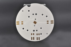
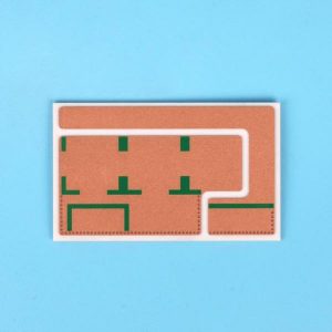
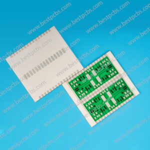
What is Active Metal Brazing (AMB) Technology?
AMB technology is developed on the basis of DBC technology, at a high temperature of about 800 ° C, AgCu solder containing active elements Ti and Zr is wetted and reacted at the interface of ceramics and metals, so as to achieve heterogeneous bonding between ceramics and metals.
Compared with traditional products, AMB ceramic PCB relies on the chemical reaction of ceramic and active metal solder paste at high temperature to achieve the combination, so its combination strength is higher, better reliability, extremely suitable for connectors or scenarios with large current load and high heat dissipation requirements. In particular, new energy vehicles, rail transit, wind power generation, photovoltaic, 5G communication and other power electronics and high-power electronic modules with demanding performance requirements have a huge demand for AMB ceramic copper clad plates. At present, this kind of product is becoming one of the mainstream products in the market.

Why use AMB Ceramic PCB?
The main benefits of AMB ceramic substrates include excellent thermal conductivity, copper layer bonding, reliability and suitability for high power and current applications. AMB ceramic substrate compared with the traditional DBC ceramic substrate, in the thermal conductivity, copper layer bonding force, reliability and other aspects of better performance, especially suitable for high temperature, high power, high heat, high reliability package requirements.
Specifically, the AMB ceramic substrate is welded between the copper foil and the ceramic substrate using a metal solder containing a small amount of active elements. This process improves the wettability of the solder to the ceramic after melting, so that the ceramic surface can be welded with the metal without metallization, thereby improving the thermal conductivity and copper layer bonding force.
In addition, the characteristics of AMB ceramic substrate with high current carrying capacity and low thermal expansion coefficient make it excellent in IGBT module, vehicle gauge main inverter, photovoltaic transformer, rail transit high voltage and other application.
What is the difference between DBC and AMB ceramic PCB?
Both DBC and AMB technologies use ceramic as the base material, but their bonding processes are different, leading to distinct performance characteristics.
- Bonding Process: DBC relies on a high-temperature process to bond copper directly onto a ceramic substrate. AMB, on the other hand, uses active metal brazing, where metals like titanium and zirconium are added to form a strong bond between the copper and ceramic.
- Thermal Conductivity: AMB ceramic PCBs are known for better thermal conductivity compared to DBC.
- Mechanical Strength: AMB ceramic PCBs typically offer superior mechanical strength due to the brazing process. The bond is more durable and reliable under extreme conditions.
- Flexibility in Design: AMB technology allows for more flexibility in terms of the shapes and sizes of copper patterns, which can be a big advantage in custom designs. DBC, while effective, can sometimes be limited in this regard.
AMB Ceramic PCB Manufacturing Process
The process of creating AMB ceramic PCBs is intricate and requires precision at every step. Here’s an overview of the key stages involved:
1. Ceramic Substrate Preparation: The first step is choosing the right ceramic substrate. Common materials include aluminum nitride and alumina, both known for their excellent thermal properties.
2. Metal Deposition: Copper is the most common metal used for AMB ceramic PCBs. However, unlike traditional methods, an active metal like titanium or zirconium is added to the copper to form a strong bond with the ceramic substrate.
3. Active Metal Brazing: The ceramic and metal are heated to a high temperature, allowing the active metals to react with both the copper and ceramic. This process forms a bond that is stronger than conventional methods like soldering or adhesion.
4. Etching and Circuit Formation: Once the copper has bonded with the ceramic, the next step is to etch the copper to create the desired circuit patterns. This is done using precise laser technology to ensure high accuracy.
5. Inspection and Testing: Quality control is vital in AMB ceramic PCB manufacturing. Each PCB is carefully inspected for defects and tested to ensure it meets the necessary performance criteria.
Types of Ceramic Substrate
Nowadays, there are four common types of ceramic substrates used in the ceramic PCB manufacturing – Al2O3, AlN, BeO and Si3N4. Let me introduce them firstly:
1. Al2O3
Al2O3 (Alumina) substrate is the most commonly used substrate material in the electronics industry. Compared with most other oxide ceramics, alumina ceramics have high strength and chemical stability, rich raw material sources, cheap prices, and are suitable for a variety of manufacturing technologies and different shape requirements.
2. BeO
BeO has a higher thermal conductivity than metal aluminum, applied to the need for high thermal conductivity, but the temperature exceeds 300°C rapidly decreases, but also due to its toxicity, greatly limiting the application of BeO ceramics.
3. Si3N4
The thermal conductivity of silicon nitride ceramic substrate 75-80W/(m·K), the thermal conductivity is indeed less than that of aluminum nitride ceramic substrate, but the bending strength of silicon nitride ceramic substrate is 2-3 times that of aluminum nitride ceramic substrate, which can improve the strength and impact resistance of silicon nitride ceramic copper-clad plate, welding thicker oxygen free copper without porcelain cracking phenomenon, and improve the reliability of the substrate.
4. AlN
AlN has several very important performance advantages: it is non-toxic; High insulation performance and high breakdown field strength (1.4×10⁷V/cm); Low dielectric constant (~ 8.8); Very high thermal conductivity (comparable to good thermal conductivity of aluminum, theoretical thermal conductivity 280W/m/K); There is an expansion coefficient matching Si (293K-773K, 4.8×10⁻⁶K-1). Only the mechanical strength of AlN ceramic material itself is slightly worse; Compared with Al2O3, the price of AlN is relatively high. However, in terms of cost performance, AlN is still much higher, because the thermal conductivity of Al2O3 (96%) is only 29W/M*K (25°C), and the thermal conductivity of AlN is as high as 180W/M*K (25°C). Therefore, for the emerging and rapidly developing high-power electronic devices required by the Internet of Things, artificial intelligence, 5G, power electronics, rail transit, new energy vehicles and other industries, especially high-power IGBT modules, aluminum nitride ceramic substrates with high thermal conductivity and high reliability will become the preferred material.
Among them, only Al2O3, AlN and Si3N4 can be MADE by AMB technology. Below is a performance table of AMB ceramic PCB made with different materials:

How Much Does an AMB PCB Cost?
The cost of an AMB ceramic PCB depends on several factors, each influencing the overall price.
- Material Choice
The type of ceramic used plays a significant role in the cost. Aluminum nitride is more expensive than alumina but offers superior thermal properties. Depending on the application, choosing the right material is key to balancing cost and performance.
- Copper Thickness
Thicker copper layers increase the price due to the additional material required. However, they also improve the current-carrying capacity, which might be necessary for high-power devices.
- Design Complexity
More intricate designs, especially those with custom shapes or numerous layers, will naturally cost more due to the precision required during manufacturing.
- Batch Size
Ordering AMB ceramic PCBs in bulk can reduce the cost per unit. This is particularly beneficial for larger companies that require high-volume production.
- Testing and Quality Assurance
Rigorous testing and quality checks are essential for AMB ceramic PCBs, especially in industries where failure is not an option. Higher standards of quality control can drive up costs but ensure greater reliability.
Challenges Facing AMB Technology
While AMB technology offers numerous advantages, it is not without its challenges. Understanding these challenges is crucial for its successful implementation in ceramic circuit boards.
1. Cost Considerations
One significant hurdle to the widespread adoption of AMB technology is cost. The materials involved in AMB, particularly the reactive filler metals, can be more expensive than traditional bonding methods. Additionally, the equipment and processes required for AMB may involve higher initial investments.
2. Process Complexity
The AMB process demands a high degree of precision and control. Factors such as temperature, environment, and timing must be meticulously managed to ensure optimal bonding quality.
3. Limited Availability of Filler Materials
The selection of suitable filler materials for AMB can be restrictive. Finding a filler that effectively bonds with various ceramics and metals while maintaining desirable mechanical and thermal properties can be a daunting task.
4. Risk of Thermal Shock
The high temperatures associated with the AMB process pose a risk of thermal shock to the ceramic substrates. If not properly managed, rapid temperature changes can lead to cracking or other failures in the ceramic material. Careful consideration of thermal profiles during the brazing process is essential to mitigate this risk.
Best Technology is a reliable Ceramic PCB manufacturer in China. We specialize in small to medium-volume PCB Manufacture, PCB Assembly and Electronic Manufacturing Services. Our product ranges from thick film ceramic PCB, thin film ceramic PCB, DPC ceramic PCB, DBC ceramic PCB, AMB ceramic PCB, HTCC ceramic PCB and LTCC ceramic PCB. Choose us, you can enjoy:
- High Quality
- Turn-key Service
- Competitive Pricing
- No MOQ & Fully Flexible
- Certificated with ISO9001, ISO13485, IATF16949, UL
- 99% On-time Delivery
- One time design successfully
- VIP sales assistant service
- WIP online checking


