pcb
Home > Blog

Posts Tagged ‘AOI testing’

How to avoid circuits issue while the production process ?
Monday, July 13th, 2020

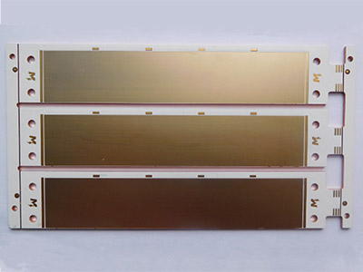
As we all know, the short & open circuits is a very common issues for the Printed Circuits Board, especially for the extra thin PCB, because its substrates thickness are very thin, generally from 0.4mm-0.15mm, so the circuits will be easy to be broken if we didn’t control the production process well.

So, you may want to know, as an experienced PCB manufacturer, what we will do to avoid the circuits issues?

Here let me show you what we do:

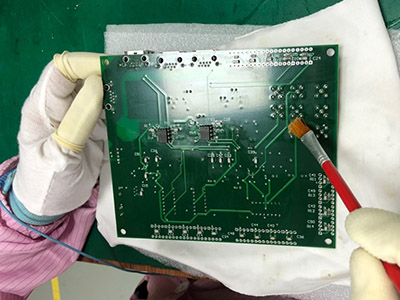
Firstly, after the process of copper plating, we will put the boards into our washing line to remove those drilling burr, surface oxide layer, etc.  To make sure the boards are fully clean before start the traces making process.
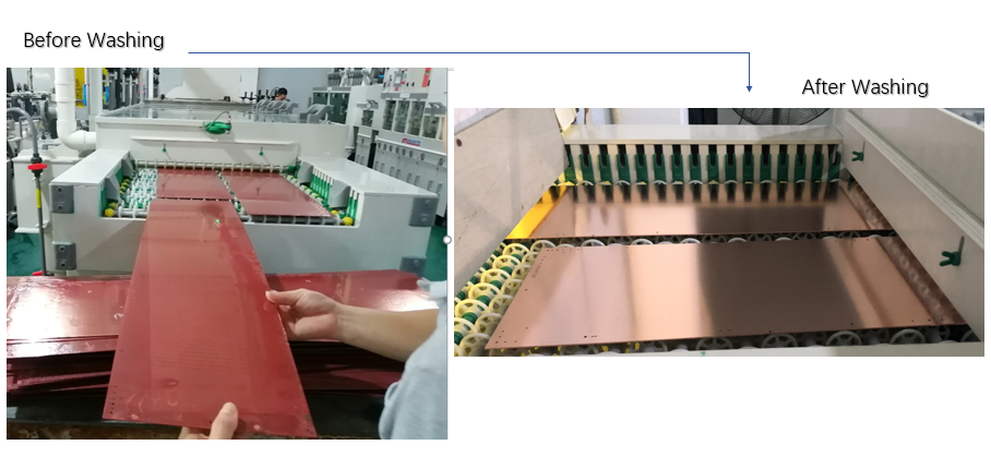
pcb washing
pcb washing

Actually, most of the open and short circuits problem are caused by the film scratching, so each operation while the pattern transfer process is very important.

That’s also why the exposure and developing need to be processed in the dust-free workshop. We will use the rack to place each PCB board separately, to avoid the touching between PCB.
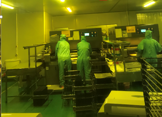
pcb explosure and developing

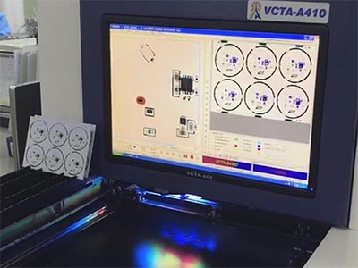
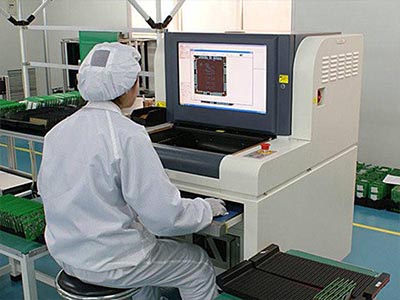
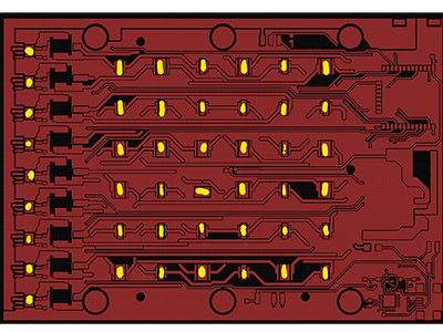
After the circuits etching out, we will take the boards to do the AOI testing, to check if there are any broken circuits, short gaps, protrusions, copper surface garbage and other problems. If there is, our machine will alert the problem, and we will fix the problem or scrap the defectives boards, with this process to prevent the defective boards move to the next step.

Most importantly is that we will do the first article inspection for all the boards, as long as we found the circuits issues while the AOI process, we will not take the whole batch boards go ahead.
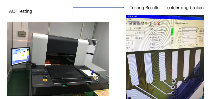
aoi testing
aoi testing

Besides, the operation standard while the etching process is also very important for how the traces being. So, our production team will control the running speed of the etching machine very strictly. If it is a PCB with o.5oz bottom copper , only allow walk 1.4 meters at per minute, if 2oz, walk 0.8m one minute.
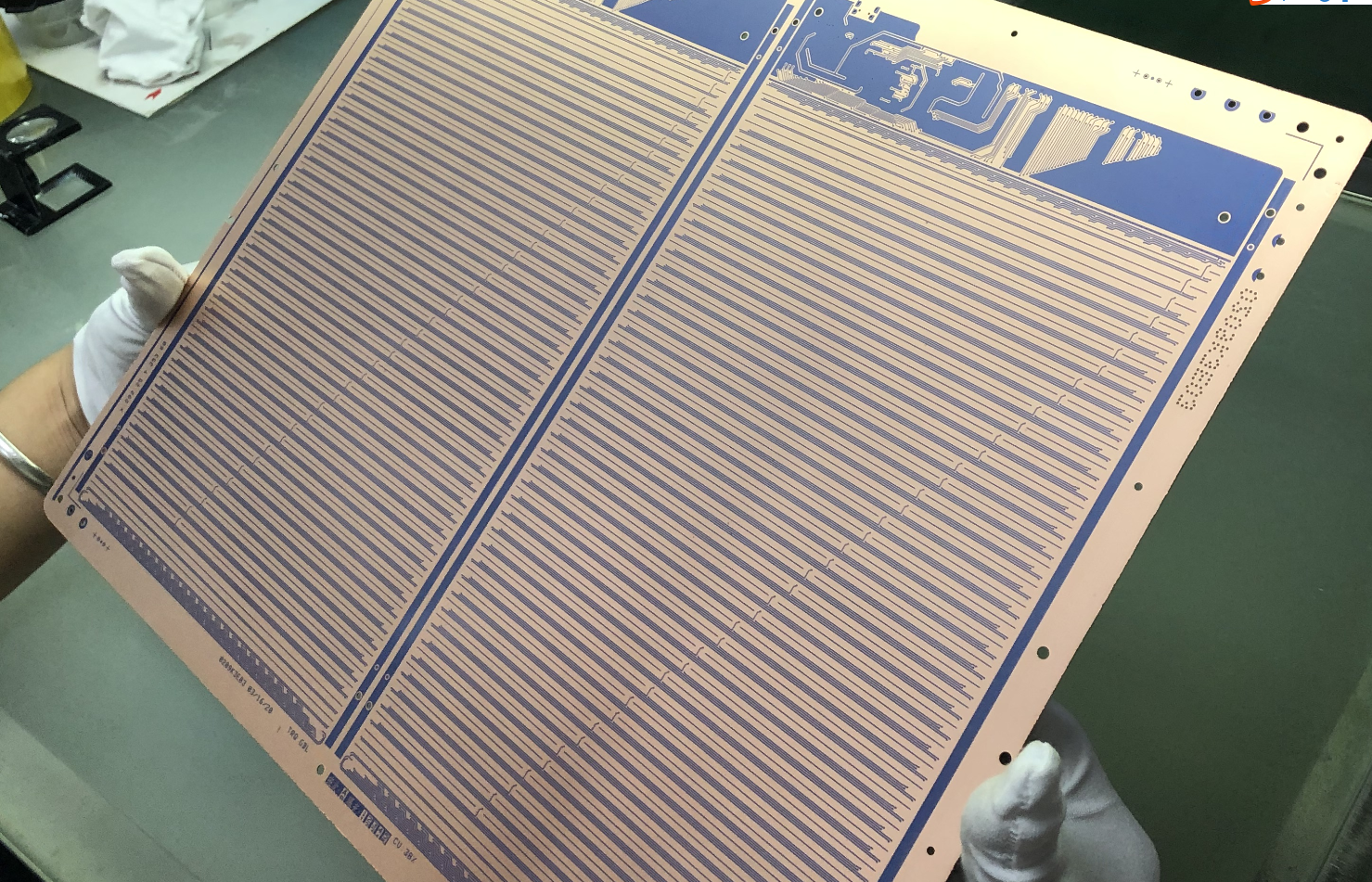
etching pcb
etching pcb

Except above process, all the boards will be required to do a final electrical testing before move to the packing. For prototypes, we will use flying probe testing. For volume, we will open the E-testing fixture to do the testing.

In our company, for the extra thin PCB, if the boards thickness lower than 0.2mm to do the flying probe testing, it needs to be tested before the outline process, because the boards are too thin to support the boards well while the flying probe, it will fall down easily.
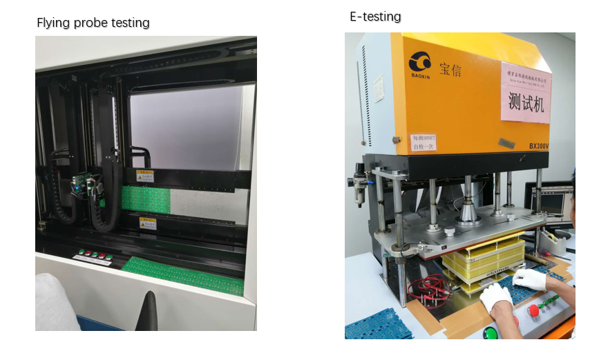
flying probe testing and electric testing

Of course, our QC people will do the double visual inspection to make sure all the boards are being well made.
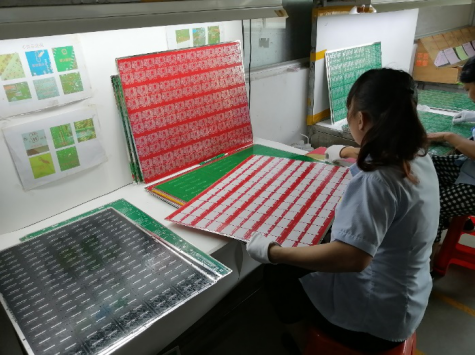
fr4 pcb inspection
fr4 pcb inspection

We always try our best effort to prevent any defective boards send to customers.  

Quality and Customers Scarification, it is always our company’s pursuit.

You may also like

The Application of AOI in Solder Paste Printing Inspection
Wednesday, December 12th, 2018

After we have talked about PCB inspection in last article, so today we move to the solder paste printing inspection. If you would like to learn something about PCB inspection, please click The Application of AOI in PCB Inspection.

AOI testing

AOI testing

Solder paste printing, the very beginning of SMT, is the root of most defects on the PCB. The defects occur in printing process is up to 60%-70%. Thus, if the defects can be avoided in this link, then the damage is able to save cost minimized. Therefore, most of printed circuit board manufacturers have already equipped with AOI testing in SMT production lines.

solder paste printing

solder paste printing

There are various of printing defects, but they can be generally divided into insufficient or excessive solder paste, the solder paste in the middle part of large pads scraped etc.. The reason why these defects are formed including unreasonable setting of printing machine parameter, low accuracy, improper selection for scraper and so on. However, it is effective to monitor the solder paste printing by AOI technology and analyze the number as well as types of defects, so that enhance the capability of printing.

Best Technology is the premier expert in manufacture of PCB and PCBA. Our unique AOI testing technology and high quality products give you a competitive supply of printed circuit board and rigid-flex circuit board. To learn more, contact us at 0755-29091601 or check our website: https://www.bestpcbs.com/

You may also like

The Application of AOI in PCB Inspection
Monday, December 10th, 2018

AOI technology possesses the functions of PCB inspection, solder paste printing inspection, component inspection and assembly inspection after welding. In this article, we mainly talk about PCB inspection.

PCB Inspection

PCB inspection are mainly relied on the visual inspection combined with electrical inspection during the early PCB production. Best Technology, on the other hand, present many benefits of AOI testing to everyone. AOI testing is a popular choice due to the following features:

√ with the development of electronic technology, the wiring density of PCB is getting higher, which increases the difficulties in visual inspection.

√ Decrease the rate of mis-judgement.

√ Able to reduce harm to the health of inspector.

√ Save cost.

√ Avoid the electronic inspection technology can not inspect some defects.

PCBA AOI testing

AOI testing

In the process of printed circuit board manufacturing, there would be some defects on the substrate fabrication and copper clad. However, these defects are mainly produced after etching. By the way, AOI testing is usually used after etching and it is utilized to find out the missing or extra part on the rigid PCB.

Most defects can be found by AOI testing (excluding the missing inspection problem), but the main problem affecting its reliability is missing inspection. The dust produced in the processing of PCB could cause false warning, so the manual inspection must be carried out after using AOI testing to detect the defects.

Best Technology is the premier expert in manufacture of PCB and PCBA. Our unique AOI testing technology and high quality products give you a competitive supply of printed circuit board and rigid-flex circuit board. To learn more, contact us at 0755-29091601 or check our website: https://www.bestpcbs.com/.  After PCB inspection, we will talk about solder paste printing inspection in the next article, if you would like to know more, please click The Application of AOI in Solder Paste Printing Inspection


You may also like