What is a BGA chip?
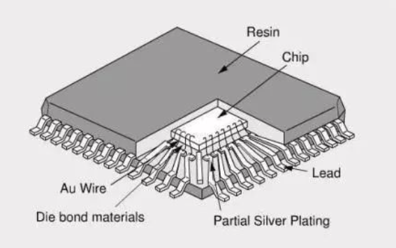
The Ball Grid Array (BGA) is actually a kind of package mode, not the chip itself. BGA is a surface adhesion technology that used in the packaging of integrated circuits, which is interconnected with the printed circuit board (PCB) by making an array solder ball at the bottom of the chip as the I/O end of the circuit. This packaging technology allows the bottom surface of the entire device to be used as a pin, with a shorter average wire length than the surrounding defined package type, resulting in better high-speed performance. BGA package technology is improved from pin grid arrays to provide more pins than other package types such as dual in-line or four-side pin flat packages. Soldering BGA-packaged devices requires precise control and is usually done by automated plant equipment. The BGA package device is not suitable for slot fixing, but is fixed to the PCB by surface mount. BGA packaging technology comes in many forms, including plastic BGA (PBGA), ceramic BGA (CBGA), and others, each of which varies in size, amount of I/O, physical structure, and packaging materials.
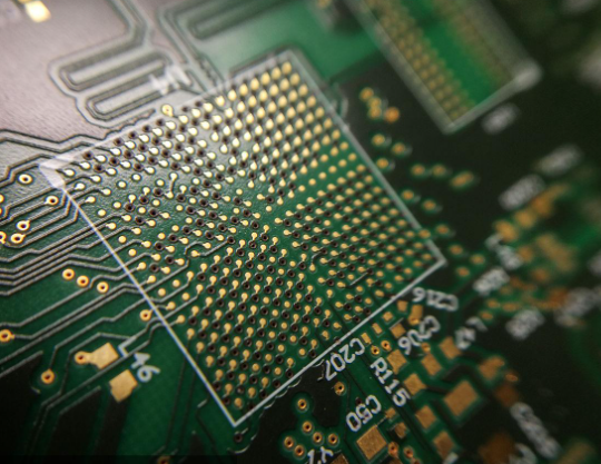
BGA Chipping Per IPC-610
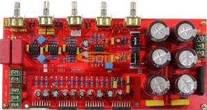
BGA chips are popular because of their compact size and ability to provide higher density connections. This allows manufacturers to pack more functionality into smaller devices. It is widely used in electronics to mount microprocessors, memory chips and other components onto printed circuit boards (PCBS), which are then installed into our electronic devices. Such as our smartphones, laptops and advanced electronic devices.
Why is BGA used?
BGA packaging is used primarily due to its ability to offer higher connection density and better electrical performance compared to traditional packages like QFP (Quad Flat Package). The design of BGAs minimizes issues like short circuits and signal interference, which are more common with older pin-based methods. Another reason BGAs are preferred is their superior thermal dissipation capabilities. The solder balls act as conductors, helping to transfer heat away from the chip. Below you can see some other benefits of using BGA chips.
1. High-density package: BGA package can provide a large number of I/O (input/output) connection points in a relatively small space.
2. Miniaturization: The BGA package allows the chip to be mounted directly on the PCB (printed circuit board), reducing the thickness and volume of the package.
3. Good heat dissipation performance: BGA package can better heat dissipation due to its large underside contact area.
4. Reliable electrical performance: BGA package adopts spherical solder joints, which can reduce signal transmission delay.
5. Easy assembly: While the number of I/O pins in the BGA package increases, the pin spacing remains unchanged or even increases, which helps to improve the yield of assembly. 6. Cost effectiveness: Although the initial investment of BGA packaging is high, it can reduce costs in the long run due to its high efficiency and miniaturization capability.
7. Wide range of applications: BGA packages are suitable for various types of integrated circuits from simple microcontrollers to complex graphics processors.
8. Easy maintenance: In some cases, BGA-packaged chips can be replaced or repaired, but this usually requires professional equipment and technology.
9. Mature technology: BGA packaging technology has been very mature, there are many types to choose from, such as PBGA (plastic ball grid array), CBGA (ceramic ball grid array), etc., to meet the needs of different applications.
What does a BGA do?
A BGA plays a crucial role in establishing electrical connections between an IC and the PCB. The tiny solder balls act as both conductors and connectors, allowing signals to flow between the chip and the board. This is critical in enabling the functionality of various devices, from computers to consumer electronics.
Additionally, BGAs enhance the durability and performance of circuits by providing a stable connection that can withstand environmental stress, such as temperature fluctuations or mechanical vibrations. This makes them a preferred choice in mission-critical applications, including aerospace, automotive, and medical electronics.
What is the difference between BGA and flip chip?
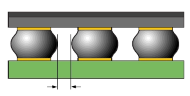
The primary difference between a BGA and a flip chip lies in how the chip is mounted onto the PCB. In a BGA, the chip is placed on top of the solder balls, which serve as the connection points between the IC and the PCB. The solder balls are positioned in a grid pattern under the chip. The chip remains on the top surface, with the balls acting as connectors below.
In contrast, a flip chip is mounted upside down, or “flipped.” The connections are made directly between the IC and the PCB, eliminating the need for solder balls. This method makes the active component of the chip face the substrate and can be directly in contact with the substrate, thus improving the thermal and electrical performance. The main advantages of flip chips include high density, which can reduce the size of the package so that more chips can be installed in a limited space. In addition, flip chip technology also has excellent electrical and thermal performance, which can provide better signal transmission and heat dissipation effects. However, it can be more expensive and complex to manufacture, making BGAs a more cost-effective solution in many cases.
BGA chipping per IPC-610
IPC-610, a globally recognized standard for PCB assembly and acceptance, provides guidelines on acceptable levels of chipping in BGAs. According to IPC-610, minor chipping on non-critical areas of a BGA is allowed as long as it does not affect the functionality or reliability of the component.
Section 10.6 of the IPC-610 standard is specific to BGA chips and defines what are acceptable and unacceptable defects. Under this standard, buyers ensure that BGA used in electronic products meets high quality standards and does not compromise the integrity of the finished product. Manufacturers must adhere to these standards to maintain the reliability and safety of their products, especially in industries such as aerospace and medical devices, where component failures can have serious consequences.
The description of BGA in IPC-A-610 standard mainly focuses on the acceptance standards of BGA components, which involve the appearance, structure, and welding quality of BGA components. Specifically, IPC-A-610 standard acceptance of BGA components includes but is not limited to the following points:
- Appearance inspection
The appearance of BGA components should meet the requirements of the standard, no obvious defects such as cracks, deformation, etc.
- Welding quality
The welding of BGA components should be uniform and complete, without bad phenomena such as virtual welding and cold welding. The solder joint should be firm and able to withstand certain mechanical stress.
- Pin/ball grid array inspection
The pin or ball grid array of the BGA component should be well docked with the PCB pad, without dislocation, offset and other phenomena. The pin or ball should be intact and free of defects.
- Size and position accuracy
The BGA component should be accurately installed on the PCB, and its position and height should meet the design requirements to ensure the normal connection of the circuit and the functional realization of the component.
In addition, as technology evolves, the IPC-A-610 standard is constantly updated to accommodate new technologies and component types. For example, the IPC-A-610G version includes new SMT terminal types and updated plating hole filling requirements, as well as BGA void requirements.
How long does IPC-610 last?
IPC-610 is regularly updated to reflect changes in technology and industry practices. However, the certification itself typically lasts for two years. After this period, manufacturers and technicians may need to undergo recertification to ensure they are up to date with the latest standards and guidelines. The two-year validity helps maintain a high level of competence and ensures that those involved in the production and inspection of PCBs follow the most current best practices.
Recertification is crucial, as it ensures that professionals stay informed about any changes in the IPC-610 standard, particularly regarding evolving technologies like BGAs and their use in modern electronics. This ongoing education helps manufacturers produce high-quality, reliable products that meet the demands of today’s fast-paced tech industry.
What is Section 10.6 of the IPC-A-610?
Section 10.6 of the IPC-A-610 standard provides specific criteria for the inspection and acceptance of BGA chipping. It outlines the types of chipping that are considered acceptable and those that are not. Minor cosmetic chips on the non-functional areas of a BGA are usually acceptable as long as they do not interfere with the operation or reliability of the chip. However, chipping on functional areas, such as those that could affect the solder ball connections, is not allowed.
What is the difference between IPC-600 and IPC-610?
IPC inspection standards refer to the inspection of electronic components according to IPC-A-600 and IPC-A-610 standards. IPC-A-600 is an inspection standard for printed circuit boards (PCBs), while IPC-A-610 is an inspection standard for electronic assembly. These two standards are the most commonly used inspection standards in the electronic manufacturing industry, which specify the appearance, size, welding quality and other requirements of electronic components.
First, the IPC-A-600 standard specifies the appearance and size requirements of the printed circuit board. According to the standard, the printed circuit board should be free of any surface defects, such as bubbles, cracks, scratches, etc. In addition, the size of the printed circuit board should meet the design requirements, the aperture, line width, line distance and other parameters must also meet the standard provisions. Only printed circuit boards that meet these requirements can be considered qualified.
Second, the IPC-A-610 standard specifies the inspection requirements for electronic assembly. According to this standard, welding quality is one of the most important inspection contents in electronic assembly. The welding should be uniform and firm, and the welding point should have no defects such as virtual welding, dislocation, short circuit and so on. In addition to the welding quality, the installation position, direction and spacing of the components also need to meet the standards. Only electronic assemblies that meet these requirements can be considered qualified.
When carrying out IPC inspection, it is necessary to carry out inspection and evaluation in strict accordance with the requirements of the standard. First of all, it is necessary to accurately understand and master the content of IPC-A-600 and IPC-A-610 standards, and understand the requirements and testing methods therein. Secondly, appropriate inspection equipment and tools should be used, such as microscopes, calipers, welding quality detectors, etc., to ensure the accuracy and reliability of the inspection. Finally, it is necessary to accurately record and evaluate the inspection results, timely discover and correct unqualified products, and ensure quality control in the production process.
With over 18 years as an industry leader, Best Technology is one of the most experienced PCB and PCB assembly manufacturer in Asia. We are highly specialized not only in quick-turn PCB prototype and PCB assembly, but also medium and small volume PCB fabrication. In Best Technology, you can enjoy a full-comprehensive one-stop service from PCB design, layout, PCB fabricate, PCB assembly, function testing and delivery. We always try our best to fabricate your PCB with copper clad laminate with the highest quality to meet your demands.
If you have any questions, please feel free to contact us with sales@bestpcbs.com, we will be happy to help you.