pcb
Home > Blog

Posts Tagged ‘Busbar PCB’

What is a PCB Board? – Best Technology
Saturday, July 13th, 2024

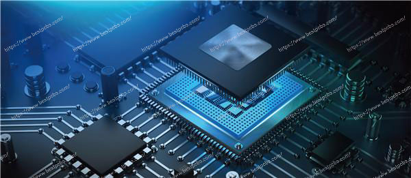
In our daily life, the electronics has been gradually infiltrated our lives. Between them, the PCB board plays an important role in it, and we must say, PCB is the foundational element of electronics. From the simplest gadgets to the most complex machinery, PCBs play a crucial role.

What is a PCB Board?

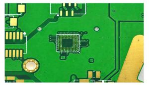
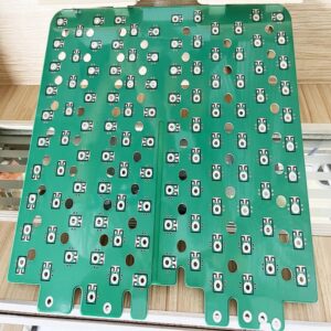
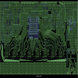
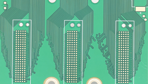
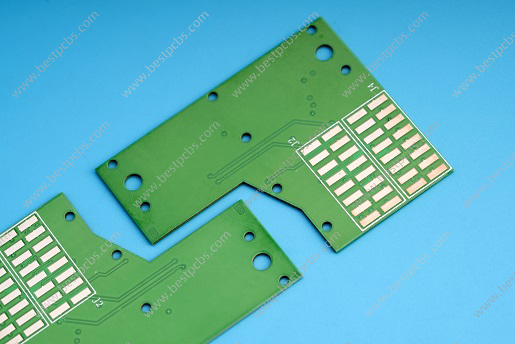
A printed circuit board (PCB) is an electronic that uses metal conductors to create electrical connections between components. Generally, a PCB is a flat, laminated composite made of non-conductive substrate materials with conductive pathways etched or printed onto it. These pathways, also known as traces, enable the electronic components mounted on the board to communicate with each other.
What is a PCB Board?

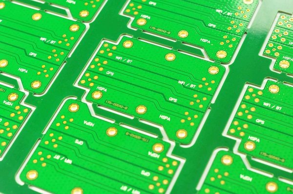
PCBs are designed to support and electrically connect various components such as resistors, capacitors, diodes, and integrated circuits. The intricate network of copper tracks forms circuits that dictate the device’s functionality. PCBs can range from simple single-sided boards used in basic electronics to complex multi-layered structures found in advanced applications.

Common PCB Structure

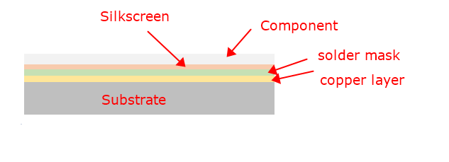
A PCB’s structure is composed of several key layers, each serving a distinct purpose. Here is a detailed breakdown of these layers:

Substrate (Base Material)

The substrate, usually made of fiberglass (FR4), provides the board with its rigidity and thickness. It is the foundational layer upon which all other materials are built.

Copper Layer

This conductive layer is typically made of copper foil. For single-sided PCBs, the copper layer is only on one side of the substrate, whereas double-sided and multi-layer PCBs have copper layers on both sides or between multiple layers of substrate.

Solder Mask

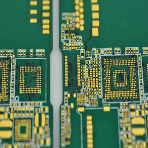
The solder mask is a protective layer applied over the copper traces to prevent oxidation and accidental short-circuiting. It insulates the copper traces and leaves the component pads exposed for soldering. The green color commonly associated with PCBs comes from this layer, though it can also be found in other colors like red, blue, black, and white.

Silkscreen

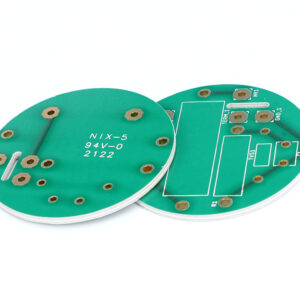
The silkscreen layer is used to add labels, symbols, logos, and other markings to the PCB. This layer helps in identifying component locations and orientations during assembly and troubleshooting.

Components and Connectors (PCBA)

Components such as resistors, capacitors, diodes, and integrated circuits are soldered onto the PCB. Connectors allow the PCB to interface with other boards, power supplies, and external devices.
What is a PCB Board?

How Many Types of PCB?

Single-Sided PCBs

These are the simplest types of PCBs, with copper on only one side of the board. You’ll find them in basic, low-cost electronics like calculators, radios, and power supplies. They’re easy to design and manufacture, which keeps costs down and makes them great for straightforward applications.

Double-Sided PCBs

These boards have copper layers on both sides, allowing for more complex circuits. They’re common in more sophisticated electronics like amplifiers, power monitoring systems, and HVAC systems. With increased circuit density and flexible design options, they can handle more complex tasks.

Multi-Layer PCBs

When you need to pack in a lot of circuits, multi-layer PCBs are the way to go. They consist of three or more layers of copper, separated by insulating layers. You’ll see these in high-tech devices like computers, servers, medical equipment, and aerospace electronics. They offer high circuit density, reduced size and weight, and better signal integrity.

Rigid PCBs

Made from solid, inflexible materials like fiberglass, rigid PCBs keep their shape and provide strong support for components. They’re durable and used in everything from simple toys to complex industrial equipment.

Flexible PCBs

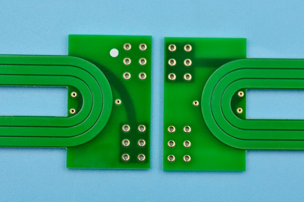
These are made from flexible plastic materials like polyimide, allowing them to bend and flex. Perfect for wearable electronics, flexible displays, and compact devices where space is tight. They’re lightweight, can fit into small, irregular spaces, and can handle being bent repeatedly.

Rigid-Flex PCBs

Combining the best of both rigid and flexible PCBs, these are great for devices that need both stability and flexibility, like smartphones, cameras, and medical devices. They save space, reduce the need for connectors and interconnections, and improve reliability.

High-Frequency PCBs

Designed to operate at frequencies above 1 GHz, these are used in communication systems, microwave technology, and high-speed devices. They provide low signal loss and high performance, making them crucial for advanced communication technologies.

Ceramic PCBs

Using ceramic as the substrate material, these PCBs offer excellent thermal conductivity and stability. They’re perfect for high-power applications and environments with extreme temperatures, like LED lighting, power electronics, and aerospace systems. Ceramic PCBs ensure reliable performance in harsh conditions.

Metal Core PCBs

Featuring a metal core, usually aluminum or copper, these PCBs improve heat dissipation. They’re used in high-power applications where efficient thermal management is crucial, such as LED lighting, power supplies, and automotive electronics.

Special PCBs

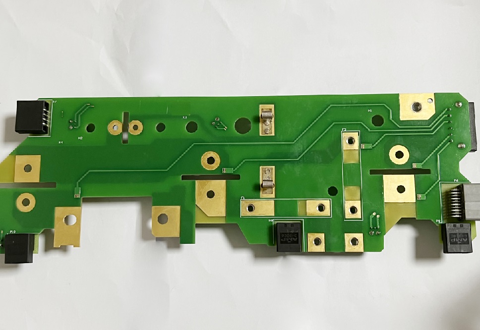
Bus Bar PCBs

These integrate bus bars for high-current applications, ensuring efficient power distribution and minimal voltage drop. They’re used in heavy-duty power supplies, electric vehicles, and industrial machinery. Bus bar PCBs provide robust and reliable connections for high-power systems.
What is a PCB Board?

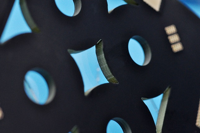
Heavy Copper PCBs

With thicker copper layers, typically 3 ounces per square foot or more, these PCBs can handle higher currents and enhance thermal management. They’re used in power distribution, automotive, and industrial applications where durability and performance are critical. Heavy copper PCBs ensure reliable operation under high-stress conditions.
What is a PCB Board?

HDI (High-Density Interconnect) PCBs

These feature finer lines and spaces, smaller vias, and higher connection pad density. They’re used in advanced electronics like smartphones, tablets, and medical devices where space and performance are paramount. HDI PCBs enable miniaturization and improved electrical performance.

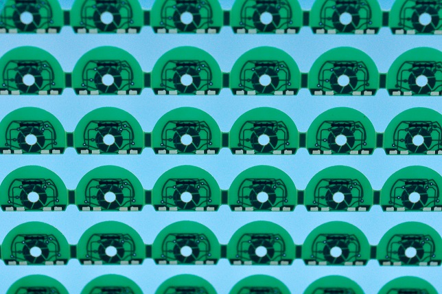
Extra Thin PCBs

Designed with minimal thickness, these PCBs are perfect for fitting into compact and lightweight devices. You’ll find them in flexible displays, wearables, and miniaturized electronic gadgets. Extra thin PCBs allow for innovative design solutions and space-saving configurations.
What is a PCB Board?

RF (Radio Frequency) PCBs

Optimized for high-frequency signals, these are used in communication devices, antennas, and microwave applications. They’re designed to minimize signal loss and interference, ensuring optimal performance in wireless communication systems.

High Tg PCBs

These have a high glass transition temperature, making them suitable for high-temperature environments. Used in automotive, aerospace, and industrial applications, high Tg PCBs maintain structural integrity and performance at elevated temperatures.

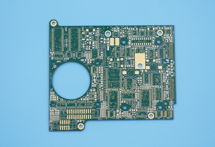
Impedance Control PCBs

These are designed to maintain consistent impedance for high-speed signal transmission. They’re used in communication devices, high-speed digital circuits, and advanced computing systems. Impedance control PCBs ensure signal integrity and reduce signal loss and reflection.
What is a PCB Board?

Why Are PCB Boards So Expensive?

Material Quality

High-grade materials like FR4 (fiberglass), ceramics, and high-quality copper foil are used to ensure durability and performance. These materials are essential for withstanding environmental stress and ensuring reliable operation, but they are expensive. For example, ceramic substrates can cost up to 10 times more than standard FR4 materials due to their superior thermal conductivity and electrical properties.

Complexity of Design

Multi-layer PCBs and advanced designs such as HDI (High-Density Interconnect) boards require complex manufacturing processes. The process involves precise alignment of layers and sophisticated techniques like laser drilling for micro-vias. The added complexity increases the production costs significantly. For instance, a standard 4-layer PCB might cost $50 per square meter, while a 12-layer HDI PCB could cost over $200 per square meter.

Precision and Technology

Manufacturing high-precision PCBs involves advanced machinery for etching, drilling, and plating. This machinery requires significant investment, and the skilled labor needed to operate it adds to the cost. The precision required in the production process ensures that the PCBs meet exacting standards, crucial for high-performance applications. A single advanced PCB drilling machine can cost upwards of $500,000.

Volume of Production

Smaller production runs generally have higher costs per unit because the setup and tooling expenses are spread over fewer units. For example, a low-volume production run of 10 PCBs might cost $100 per board, whereas a high-volume run of 10,000 boards might reduce the cost to $10 per board due to economies of scale.

Testing and Quality Assurance

Rigorous testing, including electrical, thermal, and functional tests, ensures that the PCBs meet strict performance standards. This testing process is vital to ensure reliability, especially in critical applications like medical devices and aerospace. Quality assurance processes can add 20-30% to the overall production cost, but they are essential for maintaining high standards.

What is the Difference Between PCBA and PCB Board?

The terms PCB and PCBA are often used interchangeably, but they refer to different stages of the board’s life cycle. The PCB is the bare board itself, with no electronic components attached. It consists of a non-conductive substrate, copper traces, solder mask, and silkscreen. A PCB serves as the foundation for assembling electronic components.

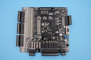
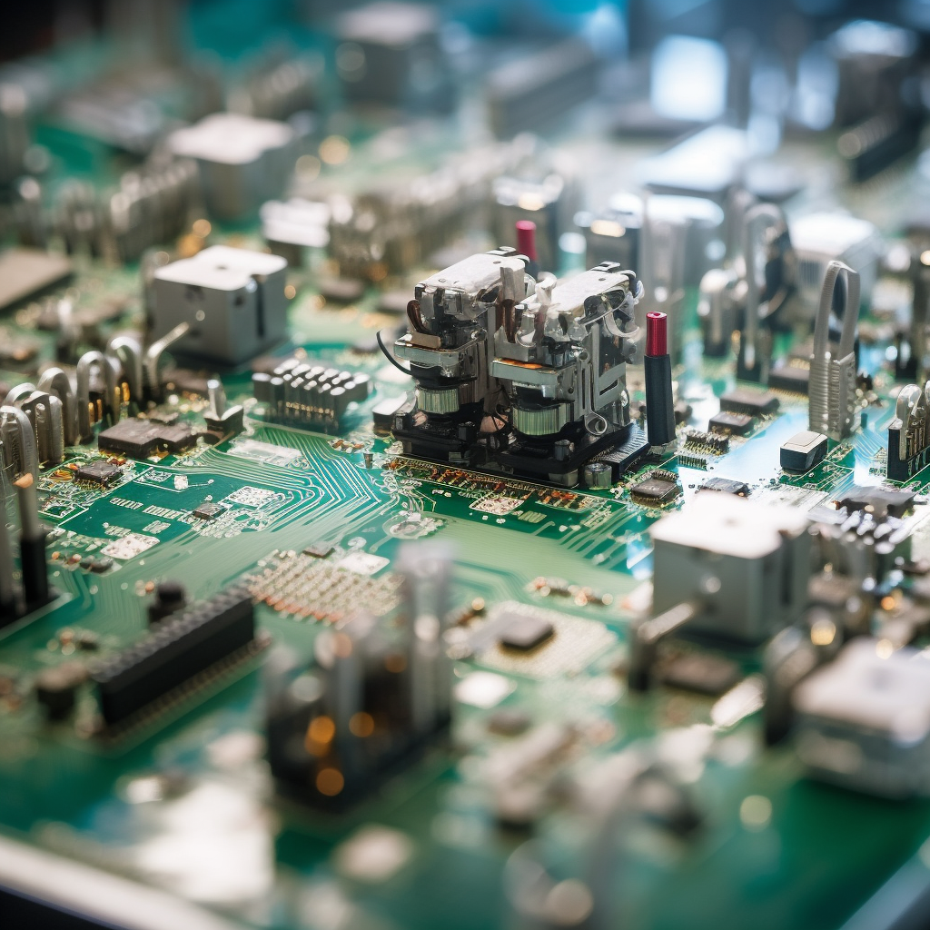
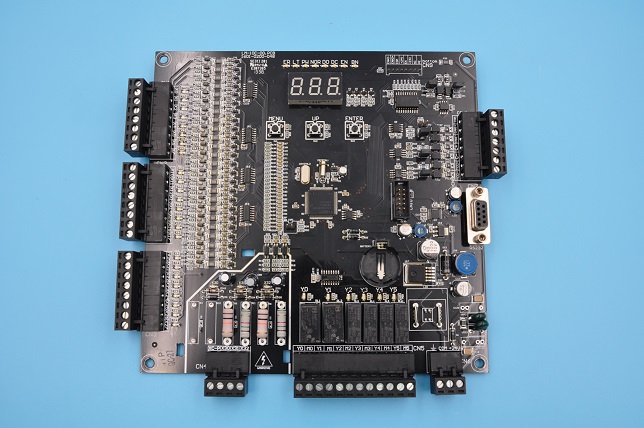
On the other hand, a PCBA (Printed Circuit Board Assembly) is a PCB that has undergone the assembly process, where all necessary electronic components like resistors, capacitors, diodes, and integrated circuits are soldered onto the board. Essentially, a PCBA is a functional circuit board ready for use in electronic devices. The transition from a PCB to a PCBA involves component placement, soldering, and quality testing, transforming the bare board into an operational assembly. Below is a typical PCBA product for your reference.
What is a PCB Board?

What is PCB Board Common Use?

PCB boards are existing in everywhere what we live, for example, the global smartphone market, which relies heavily on PCBs, was valued at approximately $520 billion in 2020. Here are some common applications that PCB used in:

Automotive Industry

In the automotive sector, PCBs are used in engine control units, infotainment systems, and advanced driver-assistance systems (ADAS). These applications enhance vehicle performance, safety, and connectivity.

Medical Devices

PCBs are integral to medical devices such as diagnostic equipment, patient monitoring systems, and implantable devices. They ensure precise and reliable operation, which is critical for patient safety and effective treatment.

Industrial Applications

PCBs are used in control systems, machinery, and power distribution units in industrial settings. They provide robust and durable solutions capable of withstanding harsh conditions and continuous operation.

Telecommunications

In telecommunications, PCBs are essential in routers, switches, and communication devices, ensuring efficient and reliable data transmission. As the demand for faster and more reliable communication networks grows, so does the need for high-quality PCBs.

Why Are Circuit Boards Green?

The characteristic green color of most PCBs comes from the solder mask, a protective layer applied over the copper traces to prevent oxidation, short-circuiting, and to protect the board during soldering.

The green color is traditional, largely due to historical reasons and practical benefits. Green solder mask provides a good contrast against the white silkscreen and the shiny copper traces, making it easier for technicians to inspect and identify components during assembly and troubleshooting. Additionally, green solder mask was one of the first colors to be developed and standardized in the industry, leading to its widespread adoption. However, PCBs are not limited to green; they can also be found in other colors such as red, blue, black, and white, depending on the specific requirements and aesthetic preferences of the project. The choice of solder mask color does not affect the performance of the PCB, but green remains popular due to its well-established manufacturing process and visual advantages.

How to Get Started with Best Technology?

Here at Best Technology, we are experienced in designing all types of PCBs, including standard rigid PCBs, special PCBs, and irregular PCBs. We can design and develop PCBs according to customer specification and offer suggestions on the right materials for your project.

We provide the full series of PCB manufacturing, from the initial PCB design, PCB layout, to custom PCB fabricate, PCB assembly, box building and so forth. By the way, we have our own factory in Vietnam, that means we can ship out the PCBs directly from Vietnam.

Welcome to contact us when you want to get a quote!

You may also like

What is Tg meaning in FR4 PCB? – Best Technology
Wednesday, July 10th, 2024

In the world of printed circuit boards (PCBs), understanding material properties is crucial. One such property is Tg, or glass transition temperature. For FR4 PCBs, knowing what Tg means can significantly impact design and performance. In this blog, we’ll explore what Tg is, how it’s measured, its importance, and other related questions.

What Does Tg Mean in PCB Manufacturing?

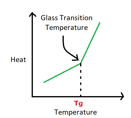
Tg stands for glass transition temperature. It refers to the temperature at which a polymer material, such as the resin in a PCB substrate, transitions from a hard, glassy state to a softer, rubbery state.

For the circuit board, the ‌Tg value reflects the highest temperature it can withstand. When the temperature exceeds Tg values, ‌ the molecular structure of the circuit board material will be changed, ‌ lead to changes in its physical properties. Such as mechanical strength, size stability, adhesive, water imbibition, thermal expansion, etc. ‌Therefore, the level of TG value of the PCB directly affects the stability and high temperature resistance of the circuit board.

What is Tg meaning in FR4 PCB? - Best Technology

In the high temperature environment, if the TG value of the circuit board is too low, it is easy to cause PCB deformation, fracture, cracking and other problems, affecting the reliability and life of the printed circuit board. If the TG value of the circuit board is too high, the PCB is easy to become hard and brittle, affecting the processability and flexibility of the circuit board.

How is Tg Measured in FR4 Materials?

Accurate measurement of Tg is crucial for ensuring the performance and reliability of FR4 PCBs. Knowing the exact Tg helps in selecting the appropriate material for specific applications, particularly those involving high temperatures and thermal cycling. Using materials with a Tg well above the operating temperature ensures the PCB will maintain its mechanical and electrical properties under expected conditions.

The primary method for measuring Tg in FR4 materials is by differential scanning calorimetry (DSC). It involves heating a small sample of the material at a controlled rate, typically between 10°C to 20°C/min. As the sample heats, the DSC measures the heat flow into the material and records it as a thermogram. The Tg is identified as the temperature where there is a noticeable change in heat capacity, appearing as a step or inflection point on the thermogram. DSC is widely used because it provides precise and reliable Tg measurements.

What is Tg meaning in FR4 PCB? - Best Technology

Additionally, Dynamic Mechanical Analysis (DMA) and Thermomechanical Analysis (TMA) also can be used to measure the Tg value.

Why is Glass Transition Temperature Critical in PCBs?

Glass transition temperature is critical because it affects the thermal and mechanical properties of the PCB. If a PCB operates near or above its Tg, it can experience issues like delamination, warping, and electrical failure. Here are some benefits of Tg.

  • Thermal stability

One of the main reasons is its role in determining thermal stability. During operation, PCBs are subjected to varying temperatures due to power dissipation from electronic components and environmental conditions. Make sure the Tg of the PCB material is well above the maximum operating temperature, it helps maintain mechanical stability and reliable performance under thermal stress.

  • Mechanical Strength

The Tg value also affects the mechanical strength and durability of the PCB. Below the Tg, the material is rigid and can withstand mechanical stress without significant deformation. This rigidity is essential for maintaining the structural integrity of the PCB, especially during assembly processes like soldering, where the board is subjected to mechanical and thermal stresses.

  • Thermal Management

Thermal management is very important to electronics, especially for those miniaturized electronic devices. If the PCB itself has good thermal management, then designers no need to install heatsink or coolers. Materials with higher Tg values exhibit lower coefficients of thermal expansion (CTE), meaning less expansion and contraction with temperature changes. 

  • Application-specific requirements

Different applications have varying thermal and mechanical requirements. High-performance computing, automotive, aerospace, and industrial electronics often operate in environments with high temperatures and thermal cycling. For these applications, using PCB materials with appropriate Tg values is crucial.

What is the Typical Tg Value for Standard FR4 PCBs?

Standard FR4 materials generally have Tg values in the range of 130°C to 140°C. For high-performance applications, materials with higher Tg values are necessary. The table below lists some common high Tg materials used in PCB manufacturing, along with their Tg values and characteristics.

MaterialTg Value (°C)CharacteristicsApplications
ISOLA IS410180Excellent thermal and mechanical propertiesHigh-reliability applications
Nanya NP-175175High thermal stability, good mechanical strengthAutomotive, industrial electronics
Shengyi S1000H170Cost-effective, widely usedConsumer electronics, industrial applications
Ventec VT-47170High Tg and low CTEHigh-density interconnect (HDI) PCBs
Rogers 4350B280Extremely high Tg, excellent thermal stabilityRF and microwave applications
(Common used high Tg materials)

Can You Explain the Difference Between Tg and Td in PCBs?

Tg and Td (decomposition temperature) are two different thermal properties. Unlike the reversible physical change associated with Tg, decomposition is an irreversible chemical process. At Td, the polymer chains in the material break down, leading to a loss of structural integrity and release of volatile compounds. Key points about Td include:

1. Chemical Stability

Td represents the upper thermal limit of a material’s chemical stability. Exceeding Td results in the breakdown of the polymer structure, rendering the material unsuitable for further use.

2. Material Selection

Knowing the Td helps in selecting materials for high-temperature applications. A material’s Td should be well above the maximum operating temperature to prevent degradation.

What is Tg meaning in FR4 PCB? - Best Technology

3. Safety and Reliability

Operating a PCB above its Td can result in catastrophic failure, including charring, delamination, and loss of electrical performance. The operating temperature remains below Td is critical for safety and reliability.

How Do You Choose the Right Tg Value for Your PCB Design?

Choosing the right Tg value depends on the operating environment and thermal demands of your application. Consider factors such as the maximum operating temperature, the thermal cycling the PCB will undergo, and the mechanical stresses it will face. Consulting with material suppliers and using simulation tools can help make an informed decision. According to our 18 years experience in PCB, we summarized a recommend Tg value for each application. Hope this is useful for you guys.

  • Consumer electronics

If your PCB will be used in standard consumer electronics, just like smartphones and tablets, a Tg value of around 130°C to 140°C is typically sufficient. These devices generally do not encounter extreme temperatures or thermal cycling.

  • Automotive applications

Automotive PCBs are always exposed to high temperatures and significant thermal cycling. A Tg value of 170°C or higher is recommended to ensure reliability and performance under the hood. So, Rogers material is good for this kind of PCB.

  • Aerospace and defense

Applications in aerospace and defense require materials that can withstand extreme temperatures and harsh environments. High Tg materials with values of 180°C or more are often used to meet these stringent requirements.

  • Industrial Electronics

Industrial environments can vary widely, but generally, high Tg materials are preferred due to the exposure to high temperatures and mechanical stress. A Tg value of at least 150°C to 170°C is advisable.

Best Technology is a well-known PCB and PCBA assembly provider in Asia and Vietnam. We have a large facility for handling low-medium to mass production PCBs, and supporting for various kinds of custom PCBs. Some special PCBs are available here, like bus bar PCB for new energy vehicles, heavy copper PCB for high power and high current PCBs, ceramic PCBs for harsh environments, extra thin PCB, RF PCB, microwaves PCB, IC substrate PCB and so on.

For more information, please do not hesitate to contact us.

You may also like

What Are the Advantages of Using Bus Bar PCB?
Friday, June 14th, 2024

In the design of electronic devices and systems, power distribution and heat dissipation management are key factors. Bus bar PCB, as an efficient solution, is particularly outstanding in these aspects. In this article, we would like to introduce the advantages of Bus bar PCB and its applications in different industries.

What Is A Bus Bar PCB?

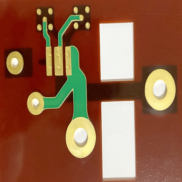
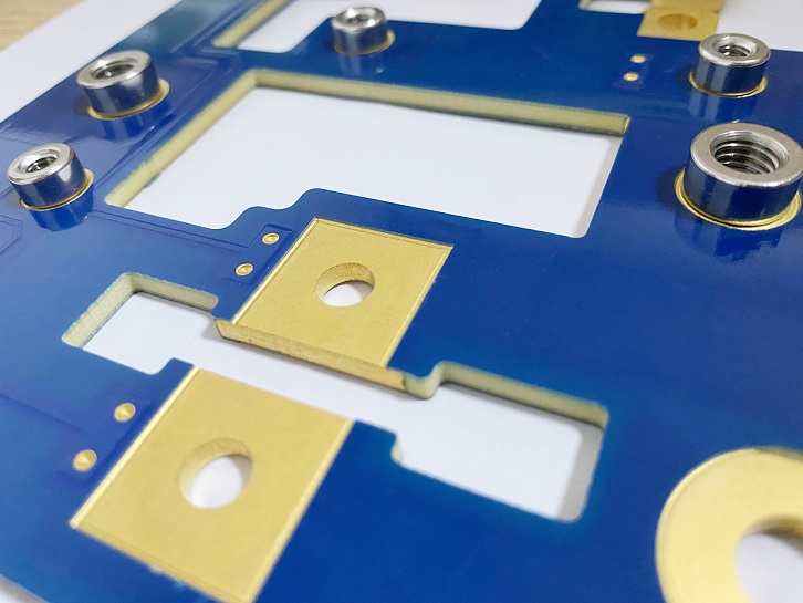
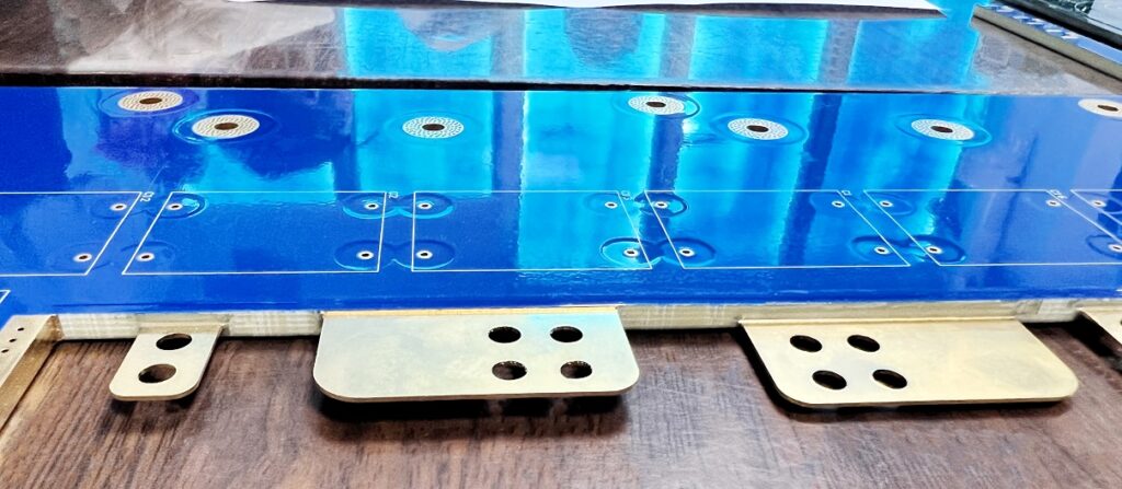
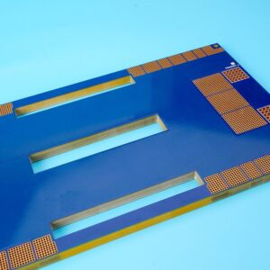
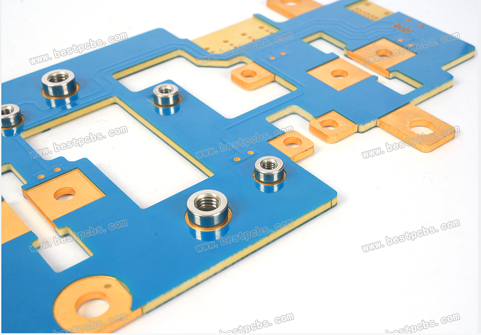
At the beginning, we should know what a bus bar PCB is. The Bus bar PCB is a special and newest design that integrates the FR4 material and metal alloy into a whole product, which allows the current transfer path into the circuit board. Due to the current carry capacity and special shape, it also called busbar PCB, embedded bus bar PCB, extruded copper PCB, copper inlay PCB, copper extrusion PCB.

bus bar pcb

Bus bar circuit board provide a more compact and efficient means of current distribution than traditional wires and cables. This design improves the overall performance of the electronic system by reducing inductance, increasing current carrying capacity, and optimizing heat dissipation.

What Are the Advantages of Bus Bar PCB?

Bus bar PCB offers numerous benefits when be using the power supply applications, its main functions are:

1. Reduce the inductance

Bus bar PCBs reduce inductance by allowing current to flow between tightly spaced conductors. This layout reduces the loop area and thus the inductance value. This is particularly important for high-frequency and highspeed applications, as it reduces voltage spikes and noise, improving system stability and performance.

2. Enhanced current carrying capacity

Due to its large cross-sectional area and high-quality conductive materials, Bus bar PCB can efficiently carry large currents. This is particularly useful in applications that require a large amount of power distribution, such as power supplies, electric vehicles, and renewable energy systems. Bus bar PCBs support higher current density compared to conventional PCB wiring, which improves thermal management and reliability.

3. Improve thermal management

The Bus bar PCB effectively dissipates heat generated by key components. In high power applications, the buildup of heat can affect performance and life. The Bus bar PCB helps maintain optimal operating temperatures through efficient heat distribution, reducing the need for additional cooling mechanisms.

4. Save space and weight

The compact design of the Bus bar PCB reduces the overall size and weight of the electronic components. Its simple construction and elimination of multiple wire connectors contribute to space savings. This is particularly beneficial for applications where size and weight are critical, such as the aerospace and automotive industries.

5. Improved reliability and durability

Bus bar PCBS have superior mechanical strength and durability compared to traditional wiring systems. Its robust construction and secure connections reduce the risk of loose connections, failure due to vibration, and mechanical wear. This improves system reliability and service life for harsh environments and demanding applications.

6. Simplify assembly and maintenance

Using a Bus bar PCB simplifies the assembly process because it reduces the number of individual wires and connectors. This not only speeds up installation, but also reduces assembly errors. In addition, the Bus bar PCB provides a more orderly and accessible layout for easy troubleshooting and repair.

embeded bus bar pcb

7. Cost effective

Although there may be a high initial cost, Bus bar PCBs can provide cost savings in the long term. Its advantages in reduced inductance, improved thermal management and enhanced reliability reduce operating and maintenance costs. In addition, Bus bar PCB reduces the need for addons, such as heat sinks or complex wiring bundles, thereby increasing overall cost effectiveness.

What Applications of Bus Bar PCB?

Due the high current carry capacity of the bus bar PCB, makes it very suitable for power supply or power management devices. Bus bar PCB can perform well in such fields. Here are some common application examples that bus bar PCB can be used for. If you are seeking for a PCB to integrate into your power supply project, then bus bar PCB is the go-to-choice.

1. Power Electronics

In power converters, inverters and high-current power supplies, Bus bar PCBS are widely used because of their ability to efficiently handle high currents and excellent thermal performance.

2. The Automobile industry

Another popular field that bus bar PCB used in is automotives, especially in electric vehicles (EVs) and hybrid electric vehicles (HEVs). In the electric cars, it can be used for battery connectivity and power distribution, contributing to weight reduction and performance improvements.

3. Renewable energy

Bus bar PCB is an environment friendly material, it is often used in solar systems, wind turbines and energy storage solutions to manage high currents and enhance reliability.

4. Industrial equipment

In industrial machinery and equipment, Busbar PCB provides powerful and efficient power distribution for motors, drives and control systems.

aluminum bus bar pcb

5. Aerospace

Bus bar PCBS are used in aerospace applications, such as avionics and power distribution systems, where size, weight and reliability are key factors.

Final Words

All in all, bus bar PCB offers significant advantages in handling high currents, improving thermal management, and providing reliable power distribution across various applications. By integrating bus bar PCBs, industries can achieve better power management, reduced system size and weight, and improved overall reliability.

Best Technology is a one-stop PCB solution provider in Asia, we offer various kinds of PCBs not only include bus bar PCB, but also Extra thin PCB, RF PCB, HDI PCB, Heavy copper PCB, Ceramic PCB, Metal Core PCB, Flex PCB and rigid flex PCB, PCBA and so more. We have more than 17 years-experience in PCB design and manufacturing, and served more than 1200 customers. Choosing Best Technology as your supplier ensures you get high quality PCBs, helping to improve the performance and competitiveness of your products. Contact us right now to customize your own PCB!

You may also like

Bus Bar PCB: What are the Considerations During Designing?
Saturday, June 8th, 2024

In the electronics industry especially for new-energy vehicles, a Bus Bar PCB plays an important role to achieve specific function. It transmits large amounts of current through metal strips or conductive paths, making it ideal for high-power applications. The design of busbar PCBs is a key technical area for designers or engineers who engaged in power distribution or who require efficient current management. In this article, we would like to share some information about the considerations during a bus bar circuit board designing, hope this may help you to design a desired PCB successfully.

What is a Bus Bar PCB?

Bus bar PCB is one of a new type of heavy copper PCB and it was made by FR4 fiber glass material and laminated with metal alloys.  It transmits electrical energy from one point to multiple output points through integrated conductive paths, which are typically made of copper or aluminum. Busbar PCBs are designed to reduce resistance and inductance, thereby maximizing current transfer efficiency and minimizing energy loss.

bus bar pcb design

Generally, if it is used in a charging pile product, there are generally at least 2 busbar circuit boards, one is the main control board (a larger one), and the other is a smaller board, both of two need to use the bus bar process.

Bus bar PCB is widely used in power distribution systems, electric vehicles, industrial equipment and other occasions requiring high current. They are designed to simplify system wiring, reduce electromagnetic interference (EMI), and improve overall reliability and performance of the product.

Why is High Current Bus Bar PCB Important?

Bus bar PCB has irreplaceable advantages in current transmission and power distribution. They mainly feature three functions when used in electronics. First of all, they are able to efficiently handle large currents without generating excessive heat. This is what standard FR4 PCB cannot achieved. Secondly, bus bar PCB has ability to significantly reduce the complexity of the circuit layout design. By integrating the current transfer path, they can reduce the number and length of circuits required by the system, thereby simplifying system design and reducing potential failures.

In addition, bus bar PCB helps reduce electromagnetic interference. Due to the design optimization of the conductive path, the noise generated during current transmission can be effectively suppressed. This characteristic makes it perform well in high-noise environments, ensuring the stability and reliability of electronic devices.

What Should We Consider When Designing A Bus Bar PCB?

Due to it is a new innovation in the industry, it is a not a simple thing to design a bus bar circuit board successfully. It’s a complex task that requires consideration of several technical factors to ensure its effectiveness and reliability. The following are the main aspects to focus on when designing a bus bar PCB.

  • Copper Thickness

The first important thing is what’s the copper thickness of busbar you want to. You must know, thicker copper allows for higher current carrying capacity, but not thicker thickness is better, it should be calculated according to the voltage and current it will used in.

  • Current capacity and temperature management

The bus bar PCB should be designed to carry the maximum expected current while keeping the temperature within a safe range. This is usually achieved by selecting the appropriate conductor material and optimizing the cross-sectional area of the conductor. For example, for 100A current requirements, a typical design would use copper strips with a thickness of 5mm to ensure that the temperature rise does not exceed 20C.

bus bar pcb design
  • Resistance and inductance

Low resistance and low inductance are key to bus bar PCB design. The shape, thickness and layout of conductors should reduce resistance and inductance as much as possible to improve the efficiency of current transmission. For example, the use of trapezoidal or flat conductors can effectively reduce inductance, thereby improving current transmission performance.

  • Electromagnetic compatibility (EMC)

Bus bar PCB design also needs to consider electromagnetic compatibility issues to ensure that it does not produce too much electromagnetic interference (EMI), while being able to resist external electromagnetic interference. By optimizing the conductor layout and using shielding materials, the electromagnetic compatibility of the bus PCB can be significantly improved.

  • Thermal management

Because bus bar PCB aims to transmit high current, thermal management is an important part of the design. The thermal design should ensure that the PCB can effectively dissipate heat and prevent overheating damage. For high power applications, radiators or active cooling are often used to ensure temperature control within design specifications.

bus bar pcb design

Best Technology Manufacturing Capability of Bus Bar PCBs

As the one of leading PCB manufacturers in China, Best Technology has exceptional capabilities in the production of busbar PCBs. Our manufacturing capabilities include high-precision metal processing technology to produce busbar PCBs with complex geometry and tight tolerances. In addition, we also have the production capacity of multi-layer bus bar PCB to meet the needs of different applications.

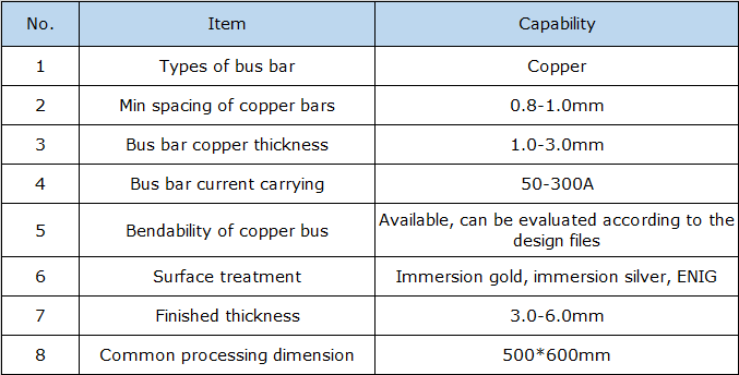
Best Technology is committed to providing customers with high-quality, high-performance busbar PCBs to support their power management and distribution systems. Below is a basic parameter of our bus bar PCB manufacturing capability. For more details, welcome to e-mail us at sales@bestpcbs.com.

Best technology capability of bus bar pcb
(Best technology capability of bus bar pcb)

Nowadays, bus bar PCBs are widely used in power distribution systems, electric vehicles, industrial equipment and other occasions requiring high current. According to statistics, the global busbar market is expected to grow at a compound annual growth rate (CAGR) of 6.5% between 2023 and 2028, demonstrating the growing importance of this technology in multiple industries.

With the rapid development of the eras, the most important thing for designers or buyers is to find a reliable bus bar PCB manufacturer to meet the high demands of the market. As the expert of the bus bar PCB fabricating, Best Technology has the mature technology and advanced equipment to produce high quality bus bar PCBs. Contact us right now to get your own bus bar PCB solutions!

You may also like

Do You Know What Is PCB Stiffener Busbar?
Wednesday, March 27th, 2024

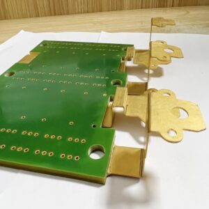
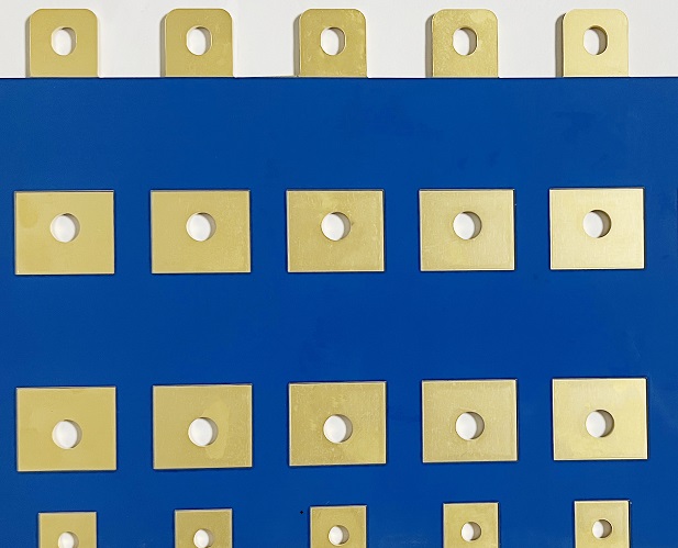
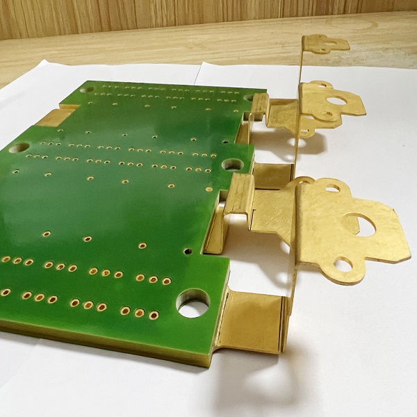
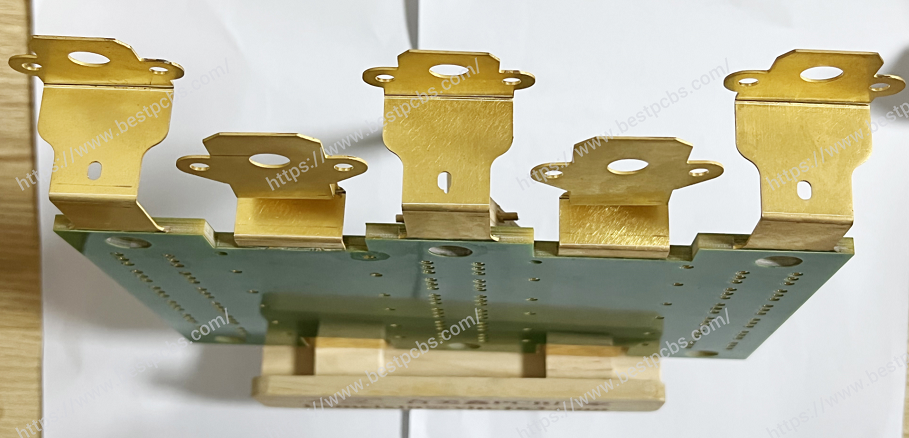
Busbar PCB is an electronic component, also known as a socket board or mother board, which is an important part of an electronic device and is used to connect and transmit current and signals, so it plays a crucial role in the design of electronic devices. Busbar PCB is like a PCB coated with an “earâ€, which we also call it as stiffener busbar. Want to know more about it? Welcome to reading on!

(Busbar_pcb)

What is PCB Stiffener Busbar?

A busbar circuit board is a key component used in electrical systems. It usually consists of a main conductive busbar (usually copper or aluminum) that is covered with an insulating material such as prepreg or resin. Busbar boards are used to transmit high currents in power systems, such as in industrial equipment, power distribution systems, and control panels.

These boards typically have multiple slots for inserting electrical connectors or electrical devices. The design of the bus board can be customized according to the specific application requirements to adapt to different current and voltage requirements. They are widely used in the industrial and commercial sectors because they provide reliable power transmission and connectivity solutions.

(Busbar_aluminum_pcb)

What Are Benefits of Using a Busbar PCB?

Busbar stiffener pcb serves as a crucial element of conducting electricity, especially when simplifying the power distribution process, saving costs and requiring greater flexibility. They come in a variety of sizes and different coatings, such as aluminum and copper. The material type, dimension, size and shape of the busbar determine the current capacity it can carry. Compared with a coil harness, though it is expensive in manufacturing, but has longer life and does not need to replace in a short time. Here we listing some benefits of busbar PCB:

  • Efficient Power Distribution

With the fast development of new energy cars and vehicles, the electronic parts in the cars also should updated to meet the demands of renewable energy powers. So the busbar PCB stands out because it can distribute the powers in devices efficiently. Meanwhile, it also can help to reducing the consumption of energy. Because of its integrated nature, it can easily adapt to the integration of renewable energy, which is quite intriguing to consider in this advanced era of energy.

  • High Conductivity

The busbar stiffener on a PCB is typically crafted from either copper or aluminum. Copper, renowned for its excellent conductivity, stands out as the preferred material for busbars due to its capacity to facilitate the flow of electrons. Moreover, copper’s robust nature enables it to withstand harsh environmental conditions and high temperatures, thus bolstering its longevity and durability. But if you want PCB that can carry higher conductivity, ceramic PCB is the best choice but a little bit higher cost.

(Busbar_copper_pcb)
  • Can be Customized

Busbar is a highly customization product in PCB design, it offers various options for its mechanical capability. So maybe you can find it in every industry, such as educations, medical instruments, factories, communications and various electronic devices. Tight space and compact devices require substitute electrical distribution, and busbars serve the purpose right. Due to its high compact and strong mechanical and chemistry, busbar PCB can be used in extremely harsh weather. This makes them a good choice in substations or devices that need to used outdoors.

  • Space Saving

Due to the copper materials mounted on the PCB, Busbar PCBs can replace multiple traces with a single, wider conductive strip, saving valuable space on the board. This compact design is particularly useful in applications where space is limited. In addition, busbar PCB provides multi-layer structure when your design is complex and has density traces network.

By means our extensive PCB & PCBA manufacturing and professional engineering team, we are highly able to build and design busbar PCBs according to your specific requirements. Meanwhile, we follow the strict quality system to make sure the high-quality of products. You are welcome to contact us or send e-mail if you want to make such busbar stiffener PCB.

You may also like