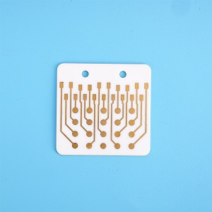
What Is a Ceramic Circuit Board?
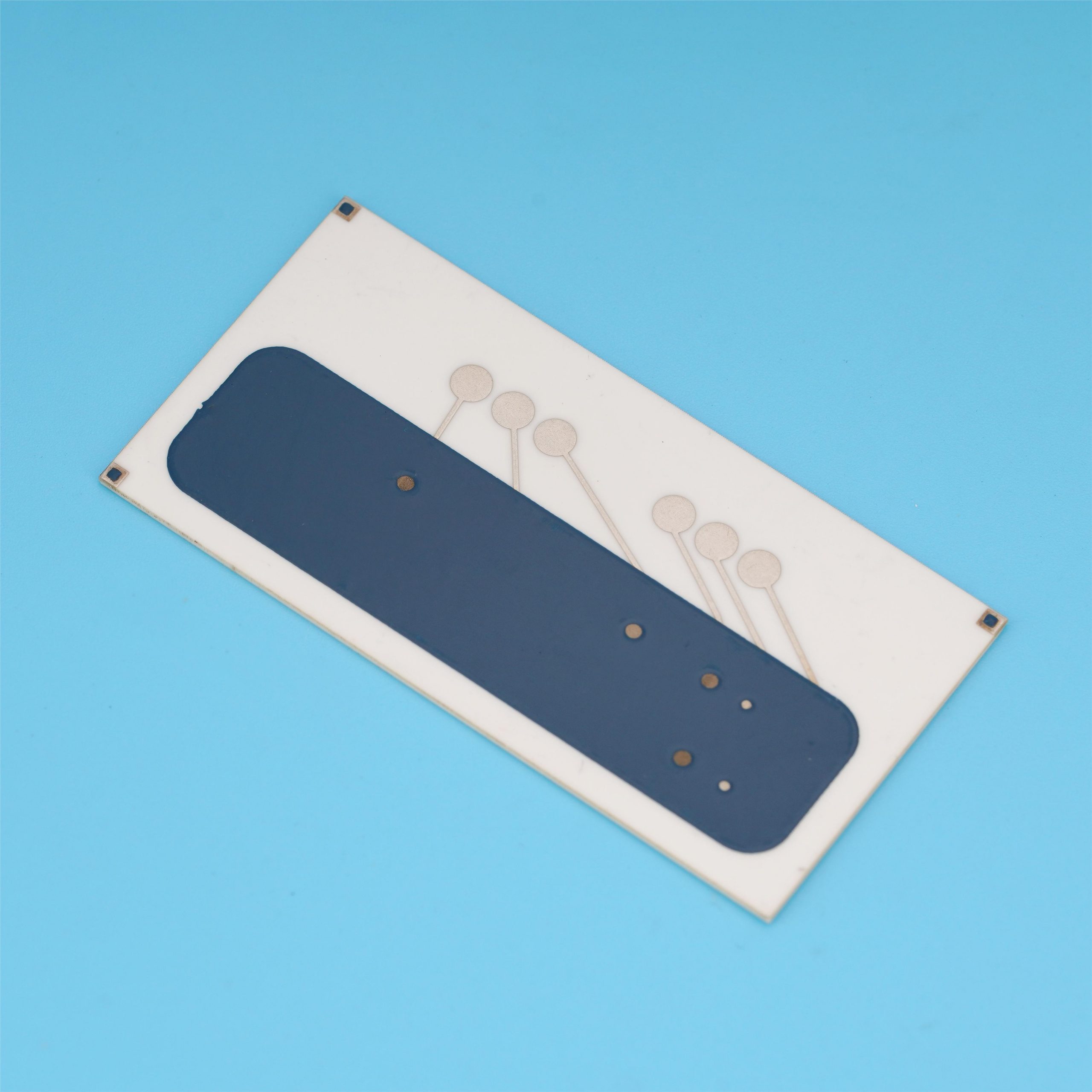
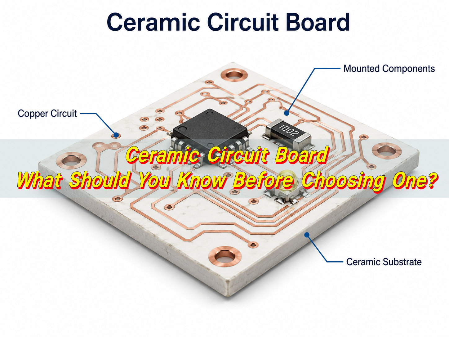
A ceramic circuit board is a printed circuit board that uses ceramic material as the insulating substrate instead of standard FR4 laminate. It supports copper circuits, carries electronic components, and helps manage heat in applications where ordinary PCB materials may not provide enough thermal or electrical performance.
Common ceramic circuit board materials include alumina, aluminum nitride, and silicon nitride. Each material has its own performance profile. Alumina is widely used because it offers a balanced combination of insulation, mechanical strength, thermal performance, and cost control. Aluminum nitride provides much higher thermal conductivity, making it suitable for high-power modules and compact thermal designs. Silicon nitride is often selected when mechanical toughness and thermal shock resistance are important.
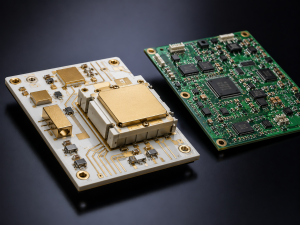
A ceramic printed circuit board is often used in products that require excellent heat dissipation, high insulation strength, stable dimensions, and long service life. Typical applications include LED modules, power electronics, automotive electronics, medical devices, RF modules, laser equipment, industrial control systems, and aerospace electronics.
Compared with standard FR4, ceramic is not selected only for appearance or premium positioning. It is chosen because the material can support more demanding electrical and thermal conditions. In high-power circuits, heat can build up around components quickly. A ceramic pcb substrate helps move that heat away from the source more effectively, improving the operating stability of the final product.
For buyers and engineers, choosing a ceramic circuit board should start with the application requirements. Important factors include working temperature, power density, voltage level, copper thickness, circuit precision, assembly method, and production volume. EBest Circuit (Best Technology) supports ceramic PCB fabrication with material guidance, DFM review, process control, testing, and assembly support, helping customers move from prototype verification to production with fewer design risks.
How Does a Ceramic Circuit Board Work?
A ceramic circuit board works by combining an electrically insulating ceramic substrate with conductive copper circuits. The ceramic base provides mechanical support and insulation. The copper layer forms the electrical path for current and signals. When components generate heat, the ceramic substrate helps transfer that heat away from the component area and toward a heatsink, housing, or cooling structure.
This working principle is important in high-power electronics. For example, in an LED module, heat is generated near the LED chip. If the heat is not removed efficiently, brightness, color stability, and service life may be affected. A ceramic circuit board improves thermal transfer because ceramic materials conduct heat much better than standard FR4. This helps keep the operating temperature more stable.
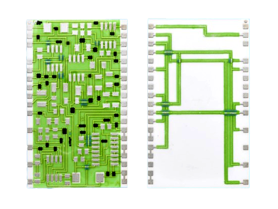
The copper layer also plays a key role. It carries electrical current, spreads heat, and connects components. Depending on the board type, copper may be plated, bonded, printed, or brazed onto the ceramic surface. The bond between copper and ceramic must be strong enough to withstand soldering temperature, thermal expansion, electrical load, and repeated operating cycles.

A ceramic printed circuit board usually works through three functional parts:
- Ceramic substrate: provides insulation, thermal transfer, and structural support.
- Copper circuit layer: carries current, signals, and heat across the board.
- Assembly layer: connects LEDs, chips, resistors, capacitors, sensors, connectors, or power devices.
The final performance depends on both material and design. Ceramic material gives the board strong thermal potential, but copper layout, substrate thickness, solder pad design, surface finish, and mounting method also affect the result. A ceramic board used in a power module, for example, needs a clear thermal path from the heat source to the cooling surface. A board used in RF equipment may need stable dimensions, tight tolerance, and controlled circuit geometry.
How Is a Ceramic Circuit Board Different from an FR4 PCB?
A ceramic circuit board and an FR4 PCB both provide electrical interconnection, but their base materials behave very differently. FR4 is made from glass fiber reinforced epoxy resin. It is widely used because it is cost-effective, easy to process, and suitable for many electronic products. Ceramic boards use inorganic ceramic substrates, which provide higher thermal conductivity, stronger insulation stability, and better dimensional control under heat.
The most important difference is thermal conductivity. Standard FR4 usually has thermal conductivity of about 0.3 W/m·K. Alumina ceramic is commonly around 20–30 W/m·K, while aluminum nitride can reach about 140–180 W/m·K, depending on material grade and production process.
FR4 remains a practical choice for many control boards, communication boards, consumer electronics, and general industrial products. Ceramic becomes more suitable when heat dissipation, high-voltage insulation, compact structure, or long-term reliability becomes a key design requirement.
| Comparison Item | Ceramic Circuit Board | FR4 PCB |
|---|---|---|
| Base Material | Alumina, aluminum nitride, silicon nitride, or other ceramic material | Glass fiber reinforced epoxy laminate |
| Thermal Conductivity | About 20–180 W/m·K depending on material | About 0.3 W/m·K |
| Electrical Insulation | Excellent for high-voltage and high-power circuits | Good for standard electronic circuits |
| Heat Resistance | Strong performance in high-temperature applications | Suitable for normal PCB operating ranges |
| Dimensional Stability | Very stable under temperature changes | More affected by heat and moisture |
| Mechanical Behavior | Hard, stable, and brittle during processing | Easier to drill, route, and laminate |
| Cost Level | Higher material and process cost | More economical for general use |
| Typical Applications | LEDs, power modules, RF devices, medical, automotive, aerospace | Control boards, consumer electronics, communication modules, general PCBA |
The right choice depends on the product environment. FR4 is suitable when the design has moderate power and enough space for thermal management. Ceramic is more suitable when the board itself must help handle heat, voltage, stability, or compact packaging. Cost should be reviewed together with the total product design. In some cases, ceramic can reduce the need for larger heatsinks or additional thermal structures.
Ceramic PCB vs FR4: Which One Should You Choose?
The choice between ceramic PCB and FR4 depends on power level, heat load, voltage requirement, product size, reliability target, and budget. FR4 is usually the preferred option for standard circuits because it offers good electrical performance, mature manufacturing, and lower cost. Ceramic circuit boards are better suited for applications that require stronger heat transfer, higher insulation strength, and stable operation under demanding conditions.

If the product is a low-power control board, sensor interface board, or general communication module, FR4 may be sufficient. If the product uses high-power LEDs, MOSFETs, IGBTs, laser diodes, RF power components, or compact power modules, ceramic should be evaluated early in the design stage.
| Selection Question | Better Fit |
|---|---|
| Is the design low power and cost-sensitive? | FR4 PCB |
| Does the board need strong heat dissipation? | Ceramic circuit board |
| Are high-power LEDs or power semiconductors used? | Ceramic circuit board |
| Is the circuit mainly digital control or low-power signal processing? | FR4 PCB |
| Is high-voltage insulation a major requirement? | Ceramic circuit board |
| Is fast and economical multilayer production the main goal? | FR4 PCB |
| Does the product need compact size with better thermal transfer? | Ceramic circuit board |
| Is the application used in automotive, medical, aerospace, or industrial power systems? | Often ceramic, depending on design requirements |
A practical material selection process should include thermal analysis, dielectric strength review, copper thickness selection, soldering method, mechanical mounting, and assembly requirements. Ceramic can provide strong performance, but it should match the actual design need. Over-specifying material may increase cost without adding meaningful value.
EBest Circuit (Best Technology) can review Gerber files, stackup information, power data, and application requirements to help determine whether ceramic, FR4, metal core PCB, or a hybrid structure is more suitable.
Why Are Ceramic Materials Used for Circuit Boards?
Ceramic materials are used for circuit boards because they combine electrical insulation, thermal conductivity, dimensional stability, and high-temperature resistance. This combination is valuable in electronic products that need to carry current while controlling heat.
In many circuits, the substrate must insulate copper traces and components from each other. At the same time, it may need to move heat away from active devices. Ceramic materials can perform both functions well. They are electrically insulating but thermally conductive, which makes them suitable for high-power and high-reliability applications.
The most common ceramic circuit board materials include alumina, aluminum nitride, and silicon nitride. Alumina is often used for LED modules, sensors, industrial electronics, and general ceramic PCB applications. Aluminum nitride is selected when thermal performance is the main concern. Silicon nitride is useful when the design needs higher mechanical strength and resistance to thermal shock.
Ceramic materials also have good chemical stability. They resist moisture, oxidation, and many harsh environments better than organic materials. Their low coefficient of thermal expansion helps reduce dimensional changes during heating and cooling. This is important for products exposed to repeated thermal cycles.
Main reasons ceramic materials are used include:
- Better heat transfer for power components, LEDs, and compact modules.
- Strong electrical insulation for high-voltage and high-density circuits.
- High temperature capability for demanding operating environments.
- Stable dimensions during thermal cycling and assembly.
- Long-term reliability for industrial, automotive, medical, and aerospace applications.
Material selection should be based on real working conditions. Alumina is a balanced option for many projects. Aluminum nitride is preferred when heat dissipation is critical. Silicon nitride is considered when strength and thermal shock performance are priorities. A ceramic pcb manufacturer should help match the material to the application instead of recommending one substrate for every project.
What Are the Main Benefits of Ceramic Circuit Boards?
The main benefits of ceramic circuit boards are stronger thermal performance, excellent insulation, stable structure, and reliable operation in demanding environments. These benefits make ceramic suitable for products where heat, power density, and service life are important.
The most recognized benefit is heat dissipation. Heat affects component performance and product reliability. A ceramic pcb substrate provides a more efficient thermal path than FR4, helping components operate within a safer temperature range. This is useful for LEDs, power semiconductors, laser modules, and high-current circuits.
Ceramic circuit boards also provide excellent electrical insulation. This is important in power supplies, inverters, battery systems, medical devices, and high-voltage electronics. The material helps separate conductive layers and supports stable operation where insulation strength is a key requirement.
Another benefit is dimensional stability. Ceramic materials expand less than many organic PCB materials when temperature changes. This helps maintain circuit accuracy, component alignment, and solder joint stability. In precision electronics, RF devices, and high-reliability modules, this stability can improve consistency.
| Benefit | Practical Value |
|---|---|
| High Thermal Conductivity | Helps remove heat from components more efficiently |
| Excellent Electrical Insulation | Supports high-voltage and high-power circuits |
| Strong Dimensional Stability | Helps maintain circuit accuracy under temperature changes |
| High Temperature Resistance | Suitable for heat-intensive applications |
| Compact Design Support | Helps reduce dependence on large thermal structures in some designs |
| Good Chemical Stability | Supports use in demanding environments |
| Long-Term Reliability | Suitable for products with extended operating life |
Ceramic circuit boards are especially valuable when multiple requirements appear together. A board may need to handle high power, remain compact, provide insulation, and operate for many years. In these cases, ceramic can offer a strong technical foundation.
EBest Circuit (Best Technology) supports customers with ceramic PCB fabrication, PCB assembly, DFM review, material selection, testing, and production-quality support. This helps engineers select the right ceramic circuit board material and avoid issues related to copper adhesion, thermal bottlenecks, tolerance control, or assembly mismatch.
How Does a Ceramic Circuit Board Help with Heat Dissipation?
A ceramic circuit board helps with heat dissipation by transferring heat from components through the substrate and toward the cooling structure. In many electronic products, heat begins at the component junction, passes through the package, moves through the solder joint, enters the copper layer, and then travels into the board. If the substrate has poor thermal conductivity, heat may remain close to the component. Ceramic improves this path because it conducts heat much more effectively than standard FR4.
This advantage is important for high-power LEDs, power modules, RF power devices, laser diodes, and compact energy systems. These products often generate concentrated heat in small areas. A ceramic substrate helps spread and conduct that heat, reducing thermal stress around critical components.
The level of heat dissipation depends on the ceramic material. Alumina provides solid thermal performance for many applications. Aluminum nitride offers much higher thermal conductivity and is used when thermal control is a top priority. Copper thickness, copper area, substrate thickness, solder pad design, and mounting method also affect the final result.
| Material | Typical Thermal Conductivity | Common Use |
|---|---|---|
| Standard FR4 | About 0.3 W/m·K | General PCB circuits |
| Alumina Ceramic | About 20–30 W/m·K | LEDs, sensors, industrial electronics, power modules |
| Aluminum Nitride Ceramic | About 140–180 W/m·K | High-power modules, laser devices, compact thermal designs |
| Copper | About 385 W/m·K | Circuit traces, heat spreading, power paths |
Thermal design should consider the full heat path. The board material is only one part of the system. Component placement, copper layout, thermal pads, solder quality, thermal interface material, heatsink contact, and housing design all influence temperature control.
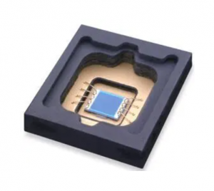
For example, a high-power LED module may use a ceramic substrate with a large copper pad under the LED. Heat moves from the LED package into the copper, through the ceramic, and then into the heatsink. If the design uses aluminum nitride, the heat transfer can be stronger, which helps compact lighting products and high-output modules.
How Are Ceramic Circuit Boards Manufactured?
Ceramic circuit boards can be manufactured through several processes, including DPC, DBC, AMB, thick film, and thin film technology. The right process depends on copper thickness, circuit precision, thermal demand, bonding strength, production volume, and application type.

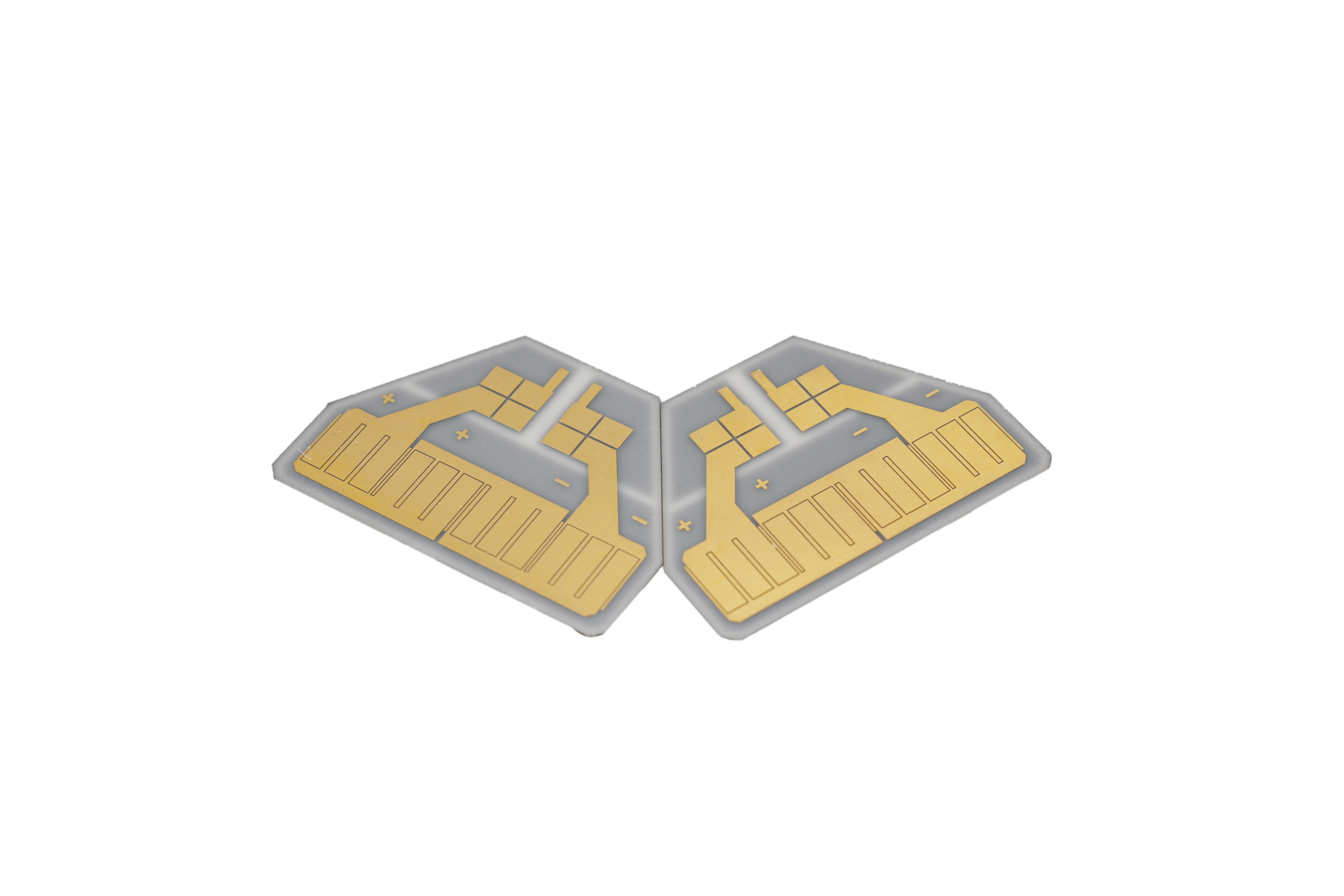
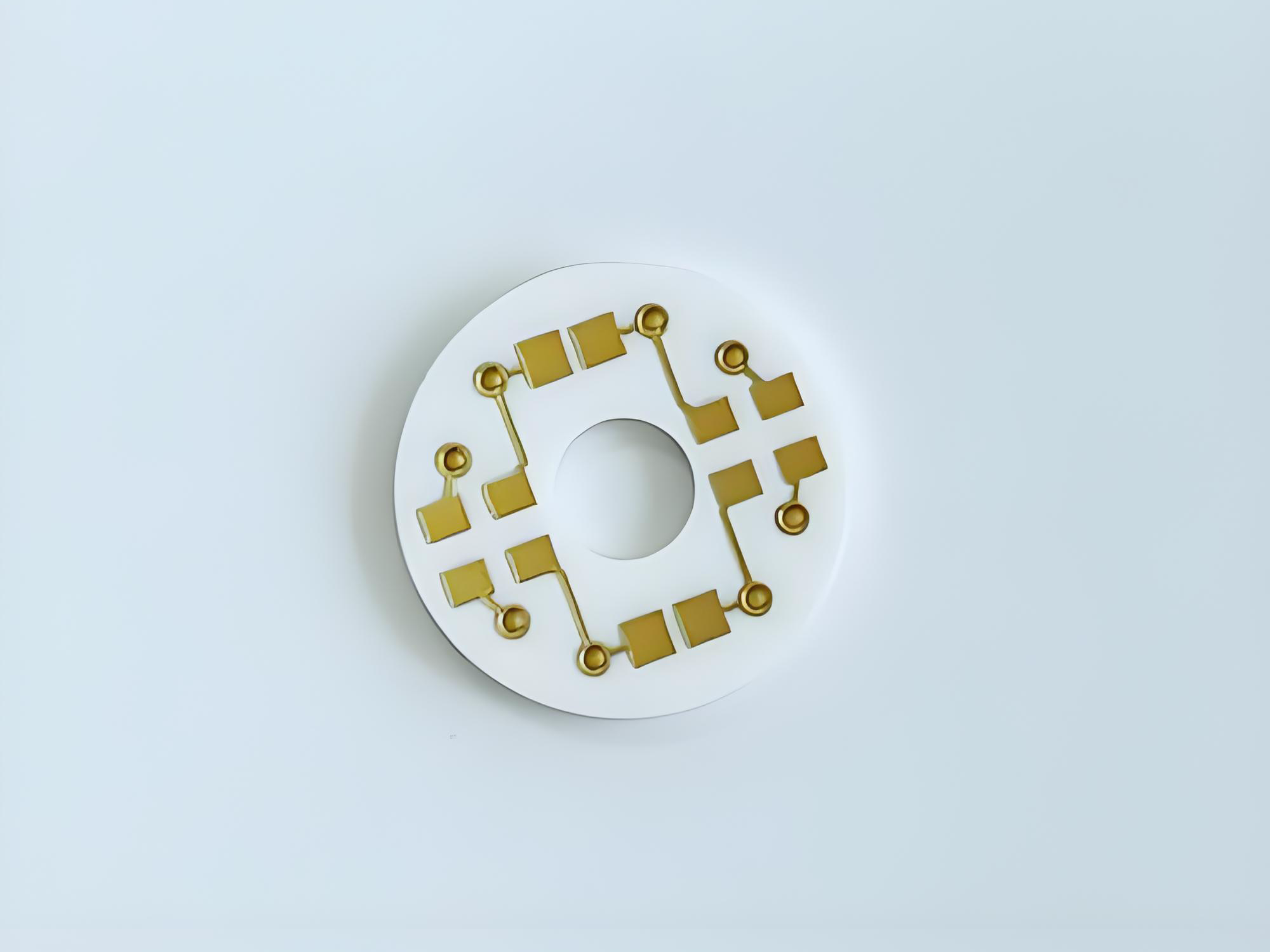
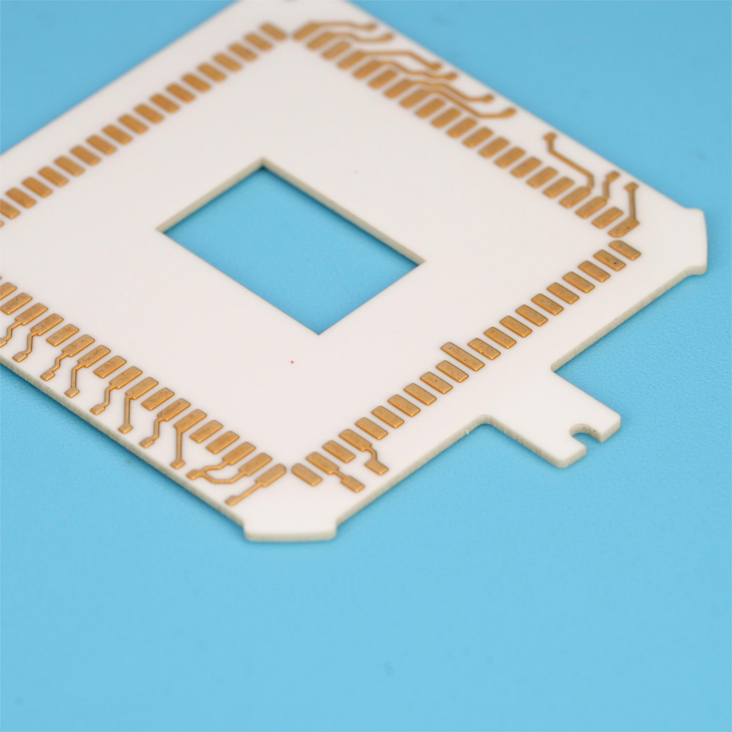
DPC, or Direct Plated Copper, is often used for fine circuits and compact ceramic PCB designs. Copper is deposited onto the ceramic substrate through metallization and plating. This process supports good pattern accuracy, smooth surface quality, and smaller circuit features. DPC is common in LED modules, sensors, RF devices, and precision electronic modules.
DBC, or Direct Bonded Copper, bonds copper foil directly to ceramic under high temperature. It supports thicker copper and higher current capacity. DBC ceramic printed circuit boards are widely used in power electronics, motor drives, inverters, automotive power systems, and industrial control equipment.
AMB, or Active Metal Brazing, uses active brazing material to bond copper and ceramic. It provides strong bonding strength and good thermal cycling performance. AMB is often selected for demanding power modules and high-reliability applications.
Thick film ceramic boards are made by printing conductive paste onto the ceramic surface and firing it at high temperature. This process is used for hybrid circuits, sensors, resistive circuits, and custom electronic modules. Thin film ceramic boards are used for high-precision circuits, RF designs, microwave products, and applications requiring stable electrical characteristics.
| Process | Main Feature | Suitable Applications |
|---|---|---|
| DPC Ceramic PCB | Fine circuits and plated copper | LEDs, sensors, RF modules, compact electronics |
| DBC Ceramic PCB | Thick copper and high current capacity | Power modules, inverters, automotive electronics |
| AMB Ceramic PCB | Strong copper-to-ceramic bonding | High-reliability power electronics |
| Thick Film Ceramic PCB | Printed conductive paste and fired circuits | Hybrid circuits, sensors, custom modules |
| Thin Film Ceramic PCB | High precision and stable electrical behavior | RF, microwave, precision circuits |
The manufacturing flow usually includes material selection, substrate preparation, cleaning, metallization, copper forming, imaging, etching, surface finishing, inspection, and testing. If the project includes assembly, SMT, chip bonding, wire bonding, or module assembly may follow.
Ceramic is harder and more brittle than FR4, so processing control is important. Cutting, drilling, laser processing, copper adhesion, surface finish, tolerance, and inspection must be managed carefully. A capable ceramic pcb manufacturer should understand both the material and the final product requirements.
EBest Circuit (Best Technology) provides ceramic PCB fabrication and PCBA support with DFM review, process evaluation, electrical testing, and production control. This helps customers reduce manufacturing risk and improve consistency from sample builds to volume production.
What Applications Use Ceramic Circuit Boards?
Ceramic circuit boards are used in applications that require reliable heat dissipation, high insulation strength, compact structure, and stable long-term performance. They are common in industries where the PCB must do more than provide basic electrical connection.
Common applications include:
- High-power LED modules and lighting systems
- Power semiconductor modules
- Automotive lighting and electronic control units
- Battery management and energy conversion systems
- RF, microwave, and radar electronics
- Medical sensors and diagnostic modules
- Industrial control and automation equipment
- Laser modules and optical electronics
- Aerospace and high-reliability electronic systems
A ceramic circuit board is a strong choice when the product needs better heat dissipation, excellent insulation, stable dimensions, and dependable long-term performance. FR4 remains suitable for many standard PCB projects, while ceramic provides a higher-performance option for thermal, power, RF, medical, automotive, and industrial applications. Before choosing one, review the ceramic circuit board material, manufacturing process, copper thickness, thermal path, voltage requirement, tolerance, and assembly method together.
For ceramic printed circuit boards, PCB fabrication, PCBA assembly, and engineering support, EBest Circuit (Best Technology) can help evaluate your design and production needs. For project consultation or quotation, contact sales@bestpcbs.com