pcb
Home > Blog

Posts Tagged ‘ceramic PCB’

Ceramic Multilayer PCB: An In-Depth Guide
星期四, 26 12 月, 2024

In the world of printed circuit board (PCB), ceramic PCB stands out as a reliable choice for applications requiring superior thermal conductivity, high-frequency performance, and robust electrical insulation. Ceramic multilayer PCB, in particular, offers an added advantage by combining multiple layers of ceramic material to enhance the performance and reliability of electronic devices. In this article, we’ll explore what ceramic PCBs is, its different types, and its specific advantages compared to other materials like FR4.

What is a Ceramic PCB?

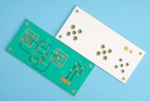
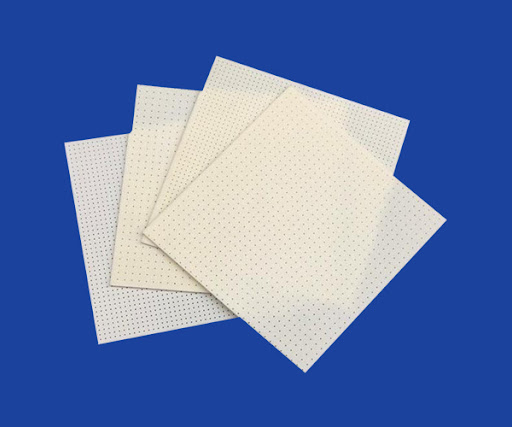
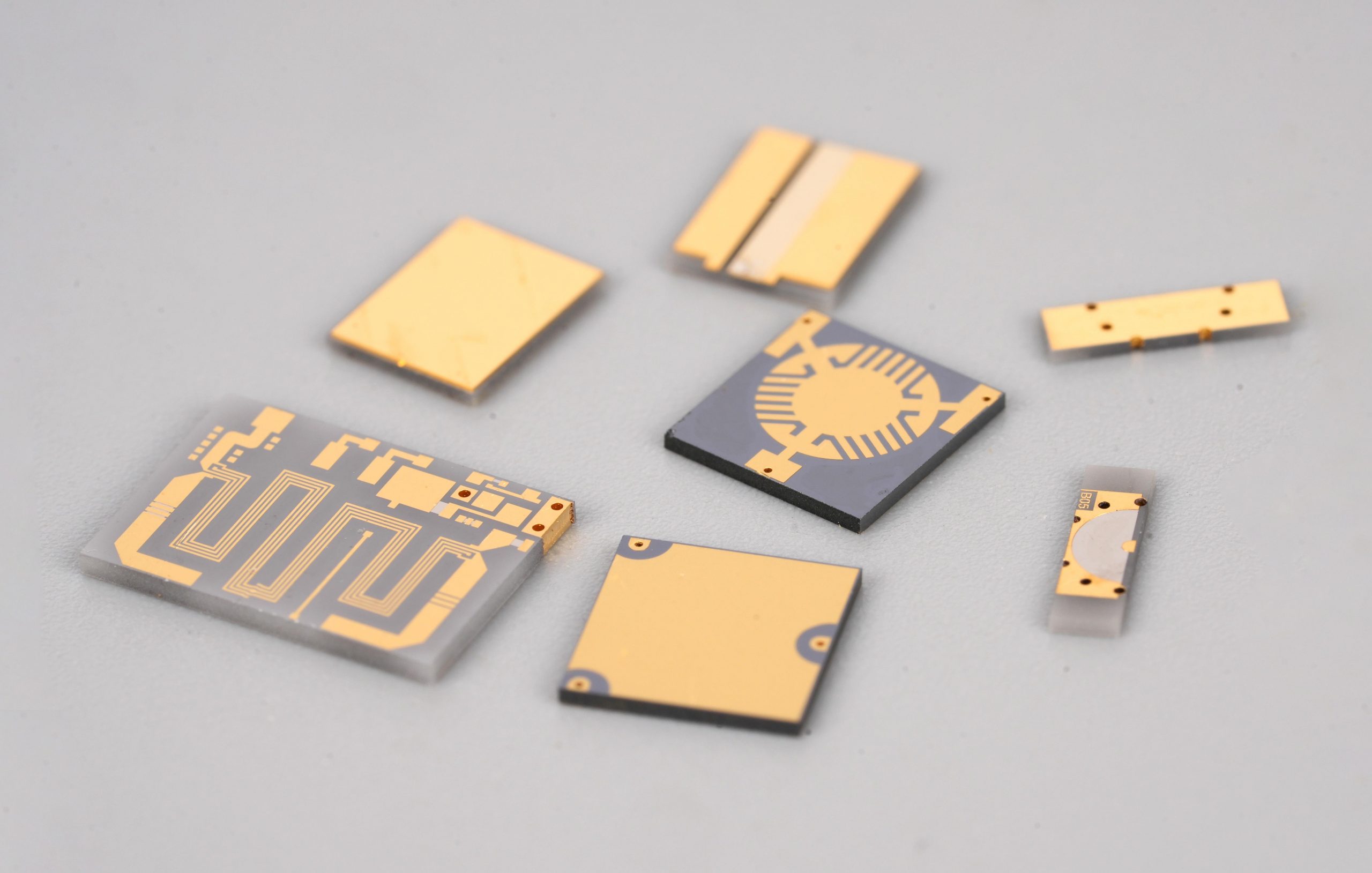
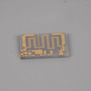
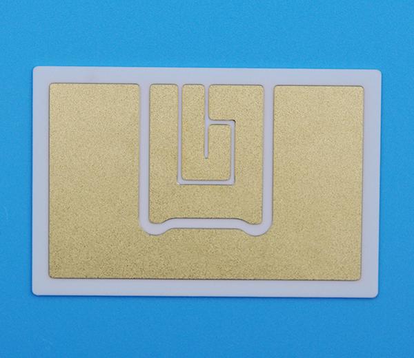
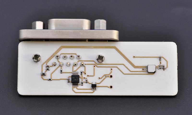
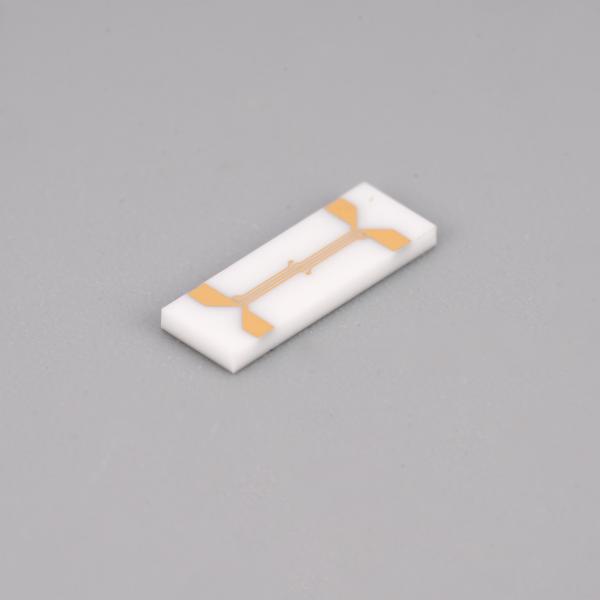
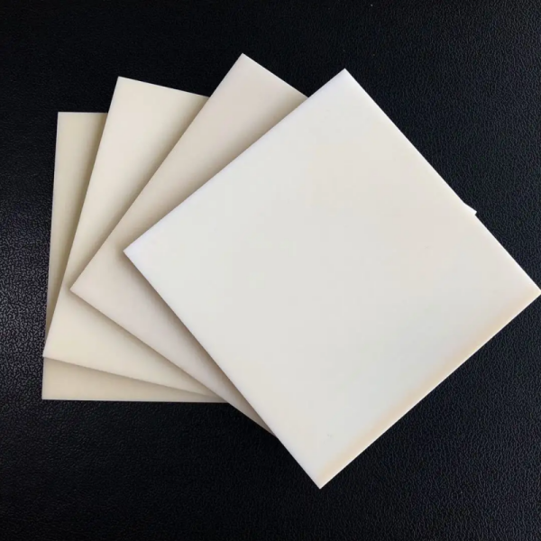
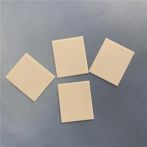
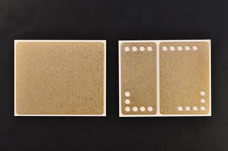
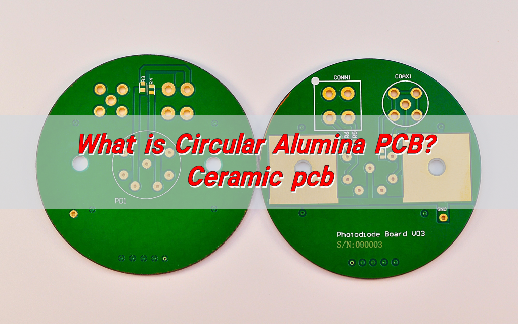
A ceramic PCB is a type of printed circuit board made using ceramic materials instead of traditional fiberglass-based boards. Ceramic substrates are known for their excellent thermal conductivity, high dielectric strength, and resistance to high temperatures. These properties make ceramic PCBs ideal for use in high-performance electronic devices that need to withstand extreme conditions.
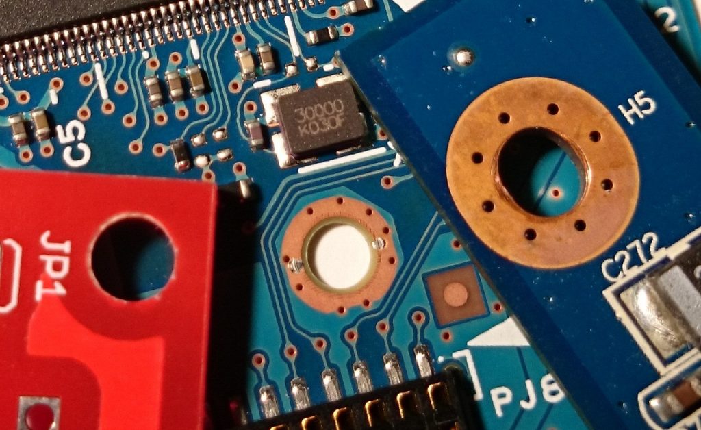
Ceramic PCB is widely used in applications like power electronics, automotive electronics, and telecommunications, where heat dissipation and stability are critical. Unlike FR4, which is a common base material for most PCBs, ceramic materials can handle much higher operating temperatures, which is essential in many industrial applications.

What Are the Different Types of Ceramic PCB?

There are several types of ceramic PCBs, each with unique properties that cater to specific needs. Here are the most commonly used:
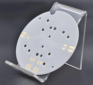
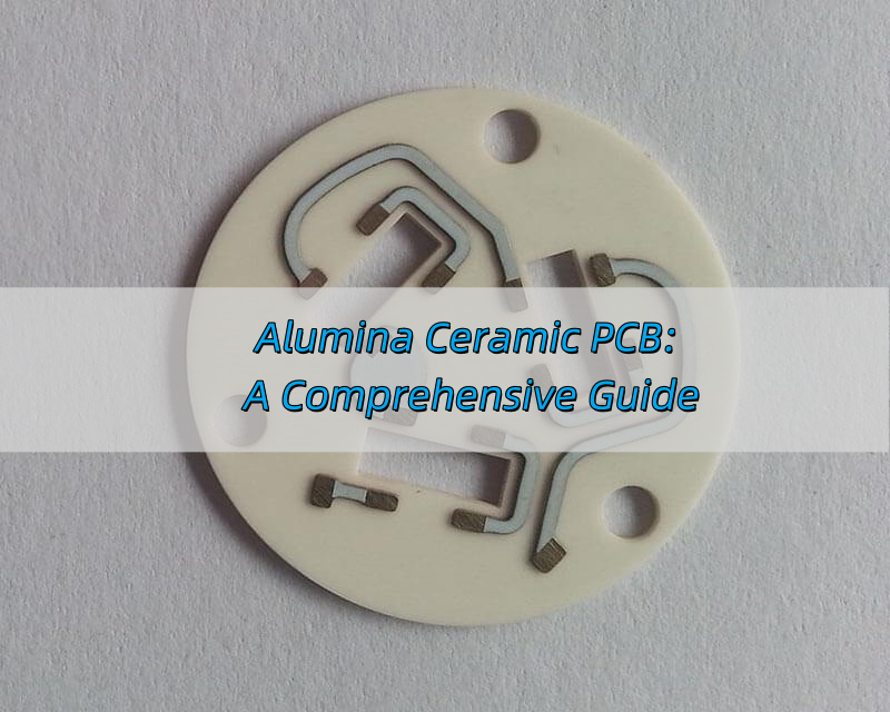
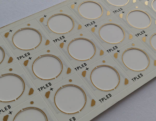
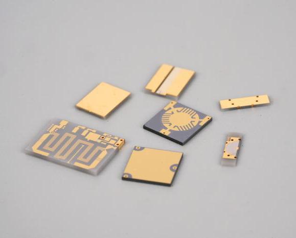
1. Alumina (Al2O3) PCBs: Alumina ceramic PCBs are the most common type. They are highly versatile and used in various applications, from consumer electronics to medical devices.
2. Aluminum Nitride (AlN) PCBs: Known for their outstanding thermal conductivity, AlN ceramic PCBs are often used in high-power applications like LED lighting, automotive systems, and power supplies.
3. Beryllium Oxide (BeO) PCBs: These PCBs are excellent in terms of thermal conductivity and electrical insulation. They are commonly used in high-frequency applications such as microwave systems.
4. Silicon Nitride (Si3N4) PCBs: These are known for their strength and thermal stability. Silicon Nitride PCBs are often used in devices that require a combination of electrical insulation and heat resistance.
Each type of ceramic material has its own set of advantages, and selecting the right one depends on factors like the operating temperature, power requirements, and the environment in which the PCB will be used.

What is the Difference Between Ceramic Substrate and FR4?

Ceramic substrates and FR4 serve similar functions in PCBs, but they differ in their material properties. FR4 is a glass-reinforced epoxy laminate, typically used in most PCBs due to its cost-effectiveness and ease of fabrication. However, it doesn’t perform well in high-temperature or high-frequency applications.
On the other hand, ceramic substrates, like alumina, have a much higher thermal conductivity and can withstand much higher temperatures, making them ideal for applications that require robust heat management. Additionally, ceramic substrates have superior electrical insulation properties compared to FR4, which is a key factor in high-power and high-voltage circuits.
In short, while FR4 is affordable and effective for everyday applications, ceramic substrates are preferred for demanding environments where thermal management and high-frequency performance are essential.

How Thick is Ceramic PCB?

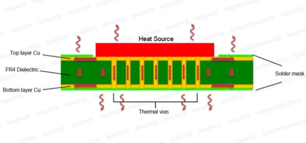
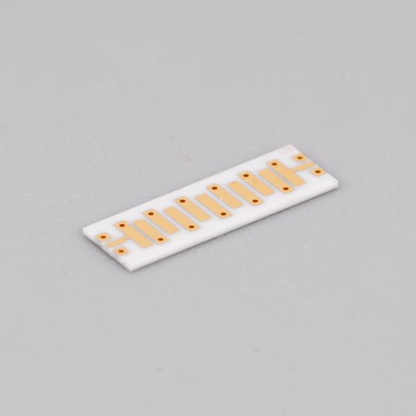
The thickness of ceramic PCBs can vary depending on the application and the type of ceramic material used. Typically, ceramic PCBs range in thickness from 0.25mm to 3.0mm, but thicker versions are possible for applications requiring more robust structural support or additional layers for signal routing.
The thickness also impacts the overall thermal conductivity of the board. Thicker ceramic PCBs provide better heat dissipation but may also reduce the flexibility for complex circuit designs. Choosing the right thickness is critical to ensure optimal performance and efficiency in the final product.

What is the Thermal Conductivity of Ceramic PCB?

One of the standout features of ceramic PCBs is their thermal conductivity. Ceramic materials like aluminum nitride, beryllium oxide, and alumina have significantly higher thermal conductivity compared to traditional PCB materials like FR4. For example, aluminum nitride has a thermal conductivity of around 170 W/m·K, while alumina is typically around 30 W/m·K.
This high thermal conductivity allows ceramic PCBs to efficiently dissipate heat, preventing overheating and damage to sensitive components in high-power applications. In contrast, FR4 has relatively low thermal conductivity, which limits its use in environments where heat management is crucial.

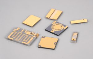
How Are Ceramic PCBs Made?

The manufacturing process of ceramic PCBs is quite different from traditional FR4-based PCBs. Here’s a simplified overview of the process:
1. Substrate Preparation: The ceramic material is first prepared, typically in the form of thin ceramic sheets. The material is chosen based on its thermal and electrical properties.
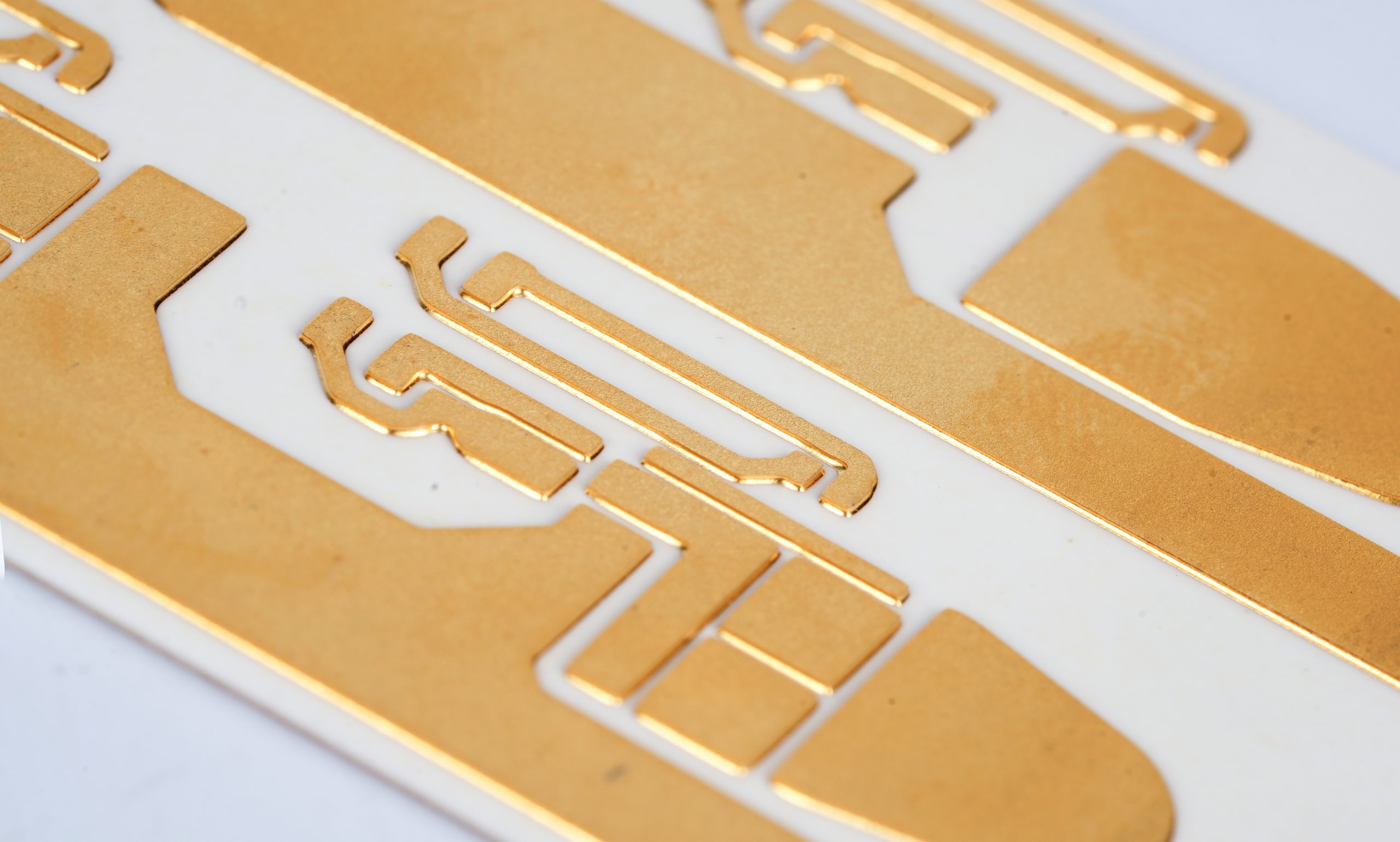
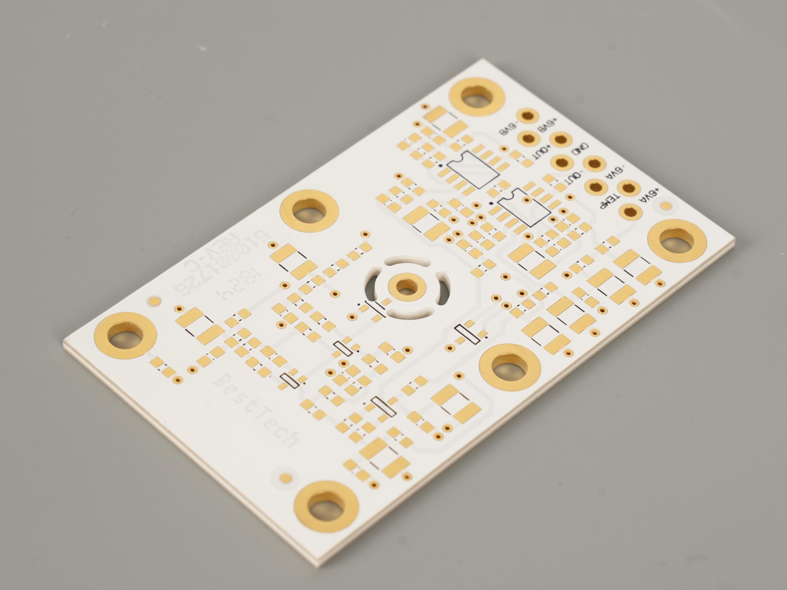
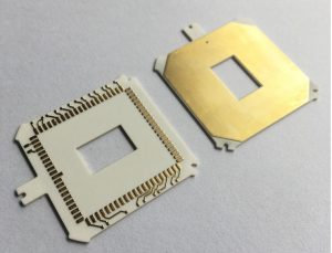
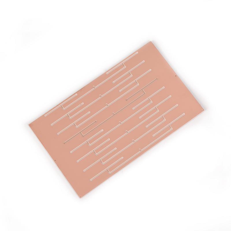
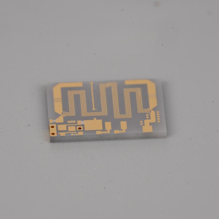
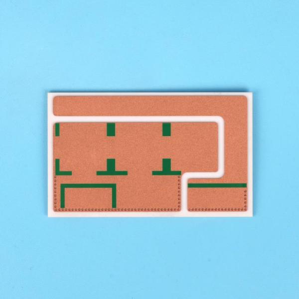
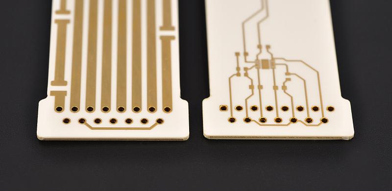
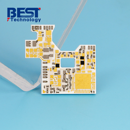
2. Layering: For multilayer ceramic PCBs, multiple layers of ceramic material are stacked together. These layers are often coated with a conductive metal layer, such as copper, to create the circuitry.
3. Etching: The copper layers are then etched to form the desired circuit pattern. This process is similar to traditional PCB manufacturing but requires special equipment due to the hardness of the ceramic materials.
4. Firing: The entire assembly is fired in a kiln to ensure that the layers bond together and the copper traces are firmly attached to the ceramic substrate.
5. Testing: Finally, the ceramic PCB is tested for electrical performance, thermal conductivity, and structural integrity. This ensures the board meets the required standards for its intended application.

What is a Ceramic Substrate Used For?

Ceramic substrates are used in a wide range of applications due to their excellent thermal management, electrical insulation, and mechanical strength. Some common uses include:
Power Electronics: Ceramic substrates are used in power semiconductors, where heat management is critical for performance.
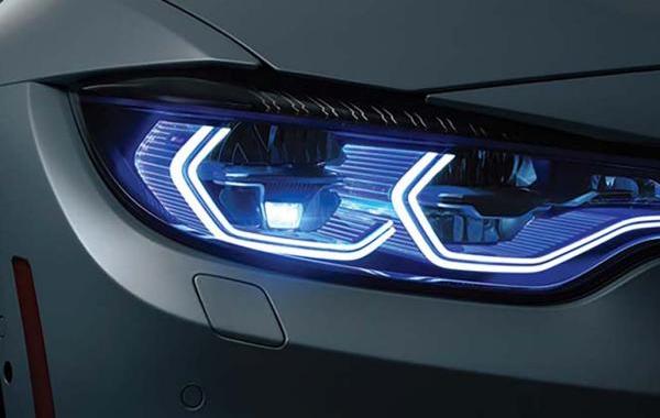
LED Lighting: The high thermal conductivity of ceramic substrates makes them perfect for LED assemblies, where efficient heat dissipation is essential for long-term reliability.
Telecommunications: Ceramic PCBs are used in high-frequency circuits, such as microwave and RF applications, where their low signal loss and thermal stability are advantageous.
Automotive Electronics: The demanding environment in automotive electronics calls for ceramic substrates that can withstand high temperatures and vibrations while ensuring reliable electrical performance.
The versatility of ceramic substrates makes them an essential component in industries that demand high-performance, reliable electronics.

Ceramic multilayer PCBs offer a range of advantages, from superior thermal conductivity to electrical insulation and high-frequency performance. They are well-suited for applications where reliability and durability are paramount, such as in power electronics, telecommunications, and automotive systems. While ceramic PCBs may be more expensive than traditional FR4 boards, their performance benefits often outweigh the cost in high-performance applications.
Whether you’re designing a high-power LED system, a complex RF circuit, or any other advanced electronic device, ceramic PCBs provide the stability, heat dissipation, and electrical insulation needed for long-lasting and efficient operation. If you’re in need of ceramic PCBs, Best Technology can provide high-quality, customized solutions tailored to your specific requirements. Reach out to us at sales@bestpcbs.com to learn more about how we can support your project with advanced ceramic PCB technology.

You may also like

Alumina Ceramic PCB: A Comprehensive Guide
星期二, 24 12 月, 2024

Alumina ceramic PCB (Printed Circuit Board) have gained significant attention in industries that demand high performance, such as electronics, medical devices, and automotive systems. Known for their excellent electrical insulation, thermal conductivity, and mechanical strength, alumina ceramics are widely used in applications that require precision and reliability. In this article, we will explore various aspects of alumina ceramics, focusing on their properties, uses, and potential benefits and drawbacks, especially in the context of PCB manufacturing.

What is Alumina Ceramic?

Alumina ceramics are produced by heating aluminum powder in a controlled environment to form a ceramic compound. The material is then used in various applications, such as semiconductors, sensors, and high-performance PCBs.

One of the reasons alumina ceramics is so popular in the electronics industry is its ability to function in harsh environments. It can withstand high temperatures and pressure without degrading, making it perfect for critical applications that require both durability and efficiency.

Can Alumina Ceramic be Machined?

Yes, alumina ceramic can be machined, but it requires specialized tools and techniques. While alumina is a hard material, it is brittle, which means it can crack or shatter if not handled carefully. Precision machining methods like laser cutting, diamond grinding, and CNC milling are commonly used to shape alumina ceramic substrates for PCBs.

Manufacturers can produce alumina ceramic PCBs with fine features, such as microvias or intricate patterns, by using these advanced machining techniques. However, the machining process can be slow and expensive due to the material’s hardness. Despite these challenges, the benefits of alumina ceramics, like their excellent insulation and heat resistance, often outweigh the machining difficulties. At Best Technology, we pride ourselves on delivering multiple types of alumina ceramic PCB products that meet your high-quality standards while maintaining fast delivery times.

What is the Temperature Rating of Alumina Ceramic?

Alumina ceramic has a high-temperature resistance, making it ideal for environments that experience heat stress. Depending on the purity and grade of alumina, its temperature rating can vary, but most alumina ceramics can withstand temperatures ranging from 1600°C to 1900°C. This makes it suitable for applications in power electronics, automotive sensors, and even space exploration.

For PCB applications, the high thermal conductivity of alumina ensures that heat generated by electronic components is efficiently dissipated, preventing damage to sensitive circuits. This property is particularly valuable in power electronics, where overheating can lead to system failures.

Is Alumina Ceramic Magnetic?

No, alumina ceramic is not magnetic. It is a non-metallic material, meaning it does not exhibit magnetic properties. This characteristic makes alumina ceramics ideal for use in electronic components that require isolation from magnetic fields. For instance, in medical devices like MRI machines, non-magnetic ceramics like alumina help avoid interference with the equipment’s functioning.

The absence of magnetic properties in alumina ceramics makes it a preferred material for PCBs used in sensitive electronic applications where magnetic interference could disrupt performance.

Is Alumina Ceramic Safe?

Yes, alumina ceramic is safe to use in a wide range of applications. As a non-toxic and stable material, it poses no significant health risks when handled properly. In fact, it is often used in medical devices, including implants and prosthetics, due to its biocompatibility.

However, like any material, alumina ceramics should be handled with care during manufacturing. Dust or particles generated from machining can be hazardous if inhaled, so it’s important to follow proper safety protocols, such as wearing protective gear and working in well-ventilated areas. Overall, alumina is a safe and reliable material in many high-performance applications.

How Strong is Alumina Ceramic?

Alumina ceramic is known for its impressive mechanical strength. It ranks among the hardest materials available, which is second only to diamond. Alumina’s compressive strength is particularly remarkable, making it highly resistant to wear, abrasion, and pressure. This makes it ideal for applications that require robust components, such as PCB substrates in electronic devices.

The material’s strength also contributes to its durability in extreme environments. For example, in high-frequency communication circuits or power electronic systems, alumina ceramics maintain their structural integrity despite thermal and mechanical stresses.

What is the Advantage of Using Alumina as a Biomaterial?

Alumina has several advantages when used as a biomaterial. Its biocompatibility makes it suitable for medical implants, such as hip replacements and dental implants. The material does not cause allergic reactions or adverse immune responses, which is crucial when used in long-term implants within the human body.

Moreover, alumina’s resistance to wear and corrosion means that it can withstand the mechanical stresses and chemical environments found in the human body. As a result, it has become a popular choice for medical devices and prosthetics. Additionally, alumina ceramics are used in various healthcare technologies like surgical tools and diagnostic devices, benefiting from their precision, durability, and sterilization capabilities.

What are the Disadvantages of Alumina Ceramic?

While alumina ceramics offer many benefits, they do have some disadvantages. One of the main drawbacks is their brittleness. Although alumina is hard, it is also prone to cracking or breaking under sudden stress or impact. This is why it is important to handle alumina ceramics carefully during manufacturing and in application.

Additionally, alumina ceramic processing can be costly. Machining this material requires specialized equipment and skills, which can make it more expensive than other materials, particularly for custom or small-batch productions. Despite these challenges, the benefits of alumina ceramics often outweigh the negatives, particularly in applications that require high performance and reliability.

In brief, alumina ceramic PCBs offer a combination of high thermal conductivity, electrical insulation, and mechanical strength, making them an excellent choice for demanding applications. Whether in high-power electronics, medical devices, or aerospace systems, alumina ceramics provide the reliability and performance needed for modern technologies.

By understanding the properties, uses, and potential drawbacks of alumina ceramic, businesses can make informed decisions about using this material in their products. Despite the machining challenges and brittleness, the advantages of alumina—such as its heat resistance, safety, and mechanical strength—make it a preferred choice in various industries.

Choosing the right material for PCB manufacturing can be complex, but alumina ceramic continues to be a top contender for those seeking durable, high-performance substrates. If you are looking for reliable PCB solutions, alumina ceramic offers the performance you need to ensure your devices operate efficiently and effectively. As a qualified alumina ceramic pcb manufacturer, Best Technology is striving to provide multiple types of PCB products without MOQ requirement for our customers. Just feel free to reach out to us via sales@bestpcbs.com to get the personalized service.

You may also like

What is the thermal conductivity of ceramic?
星期二, 8 10 月, 2024

Ceramics have emerged in many fields with their unique properties, and the thermal conductivity of ceramics has become one of the focuses of attention. Ceramic PCBs have the advantages of high thermal conductivity, good insulation performance, high mechanical strength and high precision, and have been widely used in high-power LED lighting, automotive electronics, and aerospace.

Is ceramic a good thermal conductor?

Ceramic PCB is a good thermal conductor. ‌

What is the thermal conductivity of ceramic?

The thermal conductivity of ceramic PCBs is due to the materials used, such as aluminum oxide (Al2O3) and aluminum nitride (AlN). These materials have high thermal conductivity and can effectively dissipate heat, prevent overheating, and ensure that electronic components can still work stably in high temperature environments.

The thermal conductivity of aluminum nitride reaches 170W/(mK)~220W/(mK). Such high thermal conductivity enables ceramic PCBs to effectively dissipate heat when the chip is working, ensuring that the sensor signal will not be distorted, especially in high temperature, high vibration, and corrosion environments. The signal of ceramic PCBs is still efficient, sensitive, and accurate. ‌

In addition, the manufacturing process of ceramic PCB adopts LAM technology, which is a laser rapid activation metallization technology, making ceramic PCB highly versatile and can replace the entire traditional printed circuit board with a simpler structure and enhanced performance.

In summary, ceramic PCB not only has good thermal conductivity, but also can maintain stability and reliability in harsh environments such as high temperature, high vibration, corrosion, etc., which is an ideal choice for high-performance electronic components.

What are the thermal properties of ceramics?

The thermal performance of ceramic PCB is significantly better than that of traditional printed circuit boards (PCBs).

The thermal performance of ceramic PCB is mainly reflected in the following aspects:

  • High thermal conductivity: The thermal conductivity of ceramic PCB is usually above 18W/mK, which is much higher than that of traditional ceramic materials and organic substrates. It can effectively transfer heat from the heating element to the heat sink and improve the heat dissipation efficiency.
  • Good insulation performance: The ceramic substrate has good insulation performance and can withstand high voltage and high current, ensuring the safety and stability of the circuit.
  • High mechanical strength: The ceramic substrate has high mechanical strength, can withstand large pressure and impact, and is not easy to break and deform.
  • Good chemical stability‌: Ceramic substrates have good chemical stability and can withstand corrosion from chemicals such as acids, alkalis, and salts, and are not prone to aging and deterioration‌.
  • Thin and lightweight‌: High thermal conductivity ceramic substrates can be made into thin and lightweight products to meet the needs of miniaturization and lightweight electronic devices‌.

These characteristics make ceramic PCBs the first choice for applications that generate a lot of heat and require efficient thermal management, especially in radio frequency (RF) and microwave applications, which can maintain signal integrity and minimize signal loss, making them indispensable in industries such as telecommunications, aerospace, and satellite communications‌.

In addition, ceramic PCBs’ chemical resistance and ability to withstand harsh environments make them ideal for applications that require contact with corrosive substances‌.

What material has the highest thermal conductivity?

Aluminum nitride (AlN) has the highest thermal conductivity. ‌

What is the thermal conductivity of ceramic?

Aluminum nitride (AlN) is an excellent ceramic material with extremely high thermal conductivity and low expansion coefficient. Its thermal conductivity is as high as 170-230 W/mK, making it one of the ceramic substrate materials with the best thermal conductivity.

The effective heat dissipation performance of aluminum nitride makes it particularly suitable for the heat dissipation needs of high-power density electronic devices and high-frequency electronic devices. In addition, aluminum nitride also has the characteristics of high hardness, high mechanical strength, strong corrosion resistance, high biocompatibility, and a thermal expansion coefficient close to silicon, so it performs well in applications such as high-power LEDs, power modules, and laser fields.

In contrast, other common ceramic PCB materials such as aluminum oxide (Al2O3) have low thermal conductivity, generally between 18-35 W/mK. Although they have good insulation properties and mechanical strength, their thermal conductivity is not as good as aluminum nitride and cannot meet the heat dissipation needs of high-power devices. Therefore, aluminum nitride is the preferred material in applications that require efficient heat dissipation.

What is the thermal conductivity of ceramic in W mK?

Ceramic PCB, as a high thermal conductivity material, its thermal conductivity depends on the type of ceramic substrate used. The thermal conductivity of ‌alumina ceramic‌ is between 18-35 W/mK, while the thermal conductivity of ‌aluminum nitride ceramic‌ is as high as 170-230 W/mK, which shows that aluminum nitride ceramic has higher thermal conductivity than alumina ceramic.

In addition, the thermal conductivity of ceramic PCB is better than that of traditional ‌FR4 PCB‌ or ‌metal substrate‌, the latter of which usually has a thermal conductivity of less than 3W/mK. Especially in the field of products that require high heat dissipation performance, ceramic PCB is favored for its excellent thermal conductivity.

Do ceramics have good conductivity?

The conductivity of ceramic PCB (printed circuit board) is due to the ceramic substrate it uses. This substrate material has good thermal and electrical conductivity and can withstand high power density.

Ceramic substrates are usually made of materials such as alumina, aluminum oxide and silicon nitride, which give ceramic substrates excellent electrical properties and mechanical strength, making them widely used in high-frequency communications.

The thermal conductivity of ceramic PCB is between 25~230w, with very good insulation and thermal conductivity. At the same time, its dielectric constant is low, dielectric loss is small, and it has excellent high-frequency performance. These characteristics make ceramic PCB perform well in applications that require efficient thermal management and maintain signal integrity.

How good of an insulator is ceramic?

Ceramic PCB has excellent insulation performance. ‌

What is the thermal conductivity of ceramic?

The insulation performance of ceramic PCB is due to its material characteristics. It is based on ceramic materials and has extremely high hardness and wear resistance. It also has good insulation performance and thermal stability. Ceramic materials themselves have excellent electrical insulation properties and can effectively prevent short circuits and current leakage.

Does ceramic have electrical resistance?

‌Ceramic PCB has resistance. ‌

Ceramic PCB, as a high-performance electronic substrate material, has excellent physical and electrical properties. In ceramic PCB, resistors are part of electronic components, used to limit current and reduce voltage, and are an indispensable component in the circuit. The resistors of ceramic PCBs are usually installed on the circuit board together with other electronic components to complete the function of the circuit together.

The thermal conductivity of ceramic is one of its important properties. Different types of ceramic materials have different thermal conductivities. In the future, with the continuous development and progress of electronic devices, the performance requirements for PCBs will become higher and higher, and ceramic PCBs will continue to develop and innovate to meet market demand.

You may also like

Board electronics with holes
星期五, 4 10 月, 2024

Board electronics with holes The types of vias in PCB include through holes, blind holes and buried holes, which have different characteristics and requirements in design and manufacturing. The selection of the appropriate via type should consider the number of PCB layers, wiring density, signal frequency, cost budget and production process. The via design should pay attention to avoid affecting the welding quality, preventing electrical short circuits, and saving costs in high-density packaging.

What are the holes in a PCB called?

What are the holes on PCB called? What are the holes in the circuit? The holes on PCB can be roughly divided into 3 types, screw holes (mounting holes), conductive holes (vias), and plug-in holes.

Screw holes: Screw holes are used for fixing.

Conductive holes: Conductive holes (also called vias) are used for conducting electricity just like circuits.

Plug-in holes: Plug-in holes are of course used to plug in various parts, such as diodes, transistors, capacitors, inductors, etc.

What is a through hole

What is a through hole? Through holes, also known as perforations, are holes in a PCB that go all the way through the board. Their main purpose is to provide electrical connections for component pins while allowing soldering on both sides of the board.

1.A via is a special through hole whose wall is metallized to achieve electrical connection between different layers on a circuit board. This type of hole is usually used to connect component pins to internal circuits, or to achieve electrical connection between different layers in a multi-layer PCB. Vias need to be metallized during the PCB manufacturing process, which usually includes drilling, desmearing, chemical copper plating, and electroplating.

What is a through hole

2.Non-conducting holes are the opposite of through holes. Their hole walls are not metallized, so they do not have electrical connection functions. These holes are mainly used for mechanical fixation, heat dissipation or identification purposes. Non-conducting holes are relatively simple in the PCB manufacturing process, and only drilling operations are required.

What is a through hole

What is a blind via?

A blind via is a hole that extends from one side of a PCB to a certain internal layer without penetrating the entire board. The emergence of blind vias is mainly due to the development of HDI technology, which provides circuit designers with greater flexibility and more compact layout. Blind vias are usually used to connect surface mount components (SMD) to internal circuit layers, or to connect circuits between different internal layers.

What is a blind via?

What are buried vias?

Buried vias are holes located inside the PCB that do not penetrate any side of the board. They are completely hidden inside the board and are used to connect circuits between different internal layers. Buried vias are especially useful in HDI boards because they can reduce the overall thickness of the board while maintaining electrical connections between internal circuits.

What is a microvia?

Microvia refers to a hole with a smaller diameter, usually at the micron level. The emergence of microvia technology enables PCB designers to achieve more complex circuit layouts in a smaller space. Microvias are often used in high-density, high-reliability electronic devices such as mobile phones and tablets. The manufacture of microvias requires high-precision drilling equipment and technology to ensure the accuracy and reliability of the holes.

What is a microvia?

What are Mounting holes?

What are Mounting holes?Locking holes are auxiliary holes used in the PCB manufacturing and assembly process to accurately locate and fix the circuit board. They are usually located at the edge or specific position of the PCB to ensure that the circuit board can be accurately aligned and fixed during manufacturing, testing and assembly. The locating holes do not participate in the connection of the circuit, but are essential to ensure the quality and performance of the circuit board.

What are Mounting holes?

What are Mounting holes

What are thermal vias?

Thermal vias are holes designed specifically for heat dissipation, usually large and can run through the entire PCB or multiple layers. Their role is to reduce heat buildup on the circuit board by increasing surface area and air flow, thereby improving the stability and reliability of the device. Thermal vias are particularly important in high-performance, high-power electronic devices.

What are thermal vias?

FAQ About board electronics with holes

How to solve the contradiction between manual routing and automatic routing of high-speed signals?

Most of the current powerful routing software’s automatic routing tools have set constraints to control the routing method and the number of vias. The routing engine capabilities and constraint setting items of various EDA companies are sometimes very different. For example, whether there are enough constraints to control the winding method of the serpentine, whether the routing spacing of the differential pair can be controlled, etc. This will affect whether the routing method generated by automatic routing can meet the designer’s ideas. In addition, the difficulty of manually adjusting the routing is also related to the capabilities of the routing engine. For example, the pushing ability of the routing, the pushing ability of the via, and even the pushing ability of the routing pair copper. Therefore, choosing a routing tool with strong routing engine capabilities is the solution.

Will adding test points affect the quality of high-speed signals?

As for whether it will affect the signal quality, it depends on the method of adding test points and how fast the signal is. Basically, the additional test points (not using the existing vias (via or DIP pins) as test points) may be added to the line or a small section of wire may be pulled out from the line. The former is equivalent to adding a very small capacitor to the line, while the latter is an additional branch. Both of these situations will have some impact on high-speed signals, and the extent of the impact is related to the frequency speed of the signal and the edge rate of the signal. The magnitude of the impact can be learned through simulation. In principle, the smaller the test point, the better (of course, it must meet the requirements of the test equipment) and the shorter the branch, the better.

Can you introduce some foreign technical books and data on high-speed PCB design?

Now the application of high-speed digital circuits includes communication networks and calculators and other related fields. In the communication network, the operating frequency of PCB boards has reached around GHz, and the number of layers is as many as 40 layers as far as I know. Due to the advancement of chips, the operating frequency of calculator-related applications, whether it is a general PC or server, has reached 400MHz (such as Rambus) or above. In response to the demand for high-speed and high-density routing, the demand for blind/buried vias, mircrovias and build-up process technology is gradually increasing. These design requirements can be mass-produced by manufacturers.

Does the design of rigid-flexible boards require special design software and specifications? Where can I undertake the processing of such circuit boards in China?

Can I use general PCB design software to design flexible printed circuits (Flexible Printed Circuit). The Gerber format is also used for FPC manufacturers to produce. Since the manufacturing process is different from that of general PCBs, each manufacturer will have its own restrictions on line width, line spacing, and aperture (via) based on their manufacturing capabilities. In addition, some copper foil can be laid at the turning point of the flexible circuit board for reinforcement. As for the manufacturer, you can search for “FPC” as a keyword on the Internet and you should be able to find it.

If the size of the circuit board is fixed, if the design needs to accommodate more functions, it is often necessary to increase the routing density of the PCB, but this may lead to increased mutual interference between the routings, and at the same time, the impedance cannot be reduced if the routing is too thin. Please introduce the techniques in the design of high-speed (>100MHz) high-density PCBs?

When designing high-speed and high-density PCBs, crosstalk interference does need to be paid special attention to because it has a great impact on timing and signal integrity. Here are a few things to note:

Control the continuity and matching of the characteristic impedance of the trace.

The size of the trace spacing. The spacing commonly seen is twice the line width. Through simulation, you can know the impact of trace spacing on timing and signal integrity and find the tolerable spacing. The results of different chip signals may be different.

Choose an appropriate termination method.

Avoid the same routing direction of the upper and lower adjacent layers, or even have traces overlapped up and down, because this kind of crosstalk is greater than the case of adjacent traces on the same layer.

Use blind/buried vias to increase the trace area. However, the production cost of the PCB board will increase. It is indeed difficult to achieve complete parallelism and equal length in actual implementation, but it should be done as much as possible.

In addition, differential termination and common mode termination can be reserved to mitigate the impact on timing and signal integrity.

The RF part, IF part, and even the low-frequency circuit part of the outdoor unit are often deployed on the same PCB. What are the material requirements for such PCB? How to prevent interference between RF, IF, and even low-frequency circuits?

Hybrid circuit design is a big problem. It is difficult to have a perfect solution.

Generally, RF circuits are laid out and wired as an independent single board in the system, and there will even be a special shielding cavity. Moreover, RF circuits are generally single-sided or double-sided boards, and the circuits are relatively simple. All of these are to reduce the impact on the distributed parameters of RF circuits and improve the consistency of RF systems. Compared with general FR4 materials, RF circuit boards tend to use high-Q substrates. The dielectric constant of this material is relatively small, the distributed capacitance of the transmission line is small, the impedance is high, and the signal transmission delay is small. In hybrid circuit design, although RF and digital circuits are made on the same PCB, they are generally divided into RF circuit area and digital circuit area, and laid out and wired separately. Shielding is used between ground vias and shielding boxes.

You may also like

What is an alumina circuit board?
星期五, 27 9 月, 2024

What is an alumina circuit board? As a unique circuit board material, it is emerging in the electronics field with its excellent performance and advantages. It uses alumina as the main material, bringing new opportunities for performance improvement and miniaturization of various electronic devices.

What is an alumina circuit board?

Alumina circuit board is a circuit board that uses alumina ceramic as a substrate. This circuit board has excellent electrical insulation properties, high thermal conductivity, excellent soft solderability and high adhesion strength. It can be etched with various graphics like a PCB board and has a large current carrying capacity.

What is an alumina circuit board?

Alumina ceramic circuit board is an ultra-thin composite substrate made by bonding copper foil directly to the surface (single or double sides) of an alumina (Al2O3) ceramic substrate at high temperature through a special process.

Alumina ceramic circuit boards are widely used in electronic devices that require high performance and high reliability, such as solar applications, voltage regulators, amplifier circuits, and memory modules.

Alumina ceramic substrates are mainly composed of white amorphous powder, commonly known as alumina or simply Al2O3. It has excellent properties, such as high wear resistance, acid and alkali corrosion resistance, excellent performance at high temperatures (1600-1700 degrees Celsius), etc.

What types of alumina circuit boards are there?

Ordinary alumina ceramics are classified according to their Al2O3 content, including 99%, 96%, etc. 99% alumina has high purity, white or ivory color, and is widely used in various applications, including lamps, electronic devices, and wear-resistant components. 96% alumina is widely used in various electronic applications while providing good thermal conductivity and insulation properties.

‌96% alumina‌:

  • Suitable for thick film circuit substrates, with excellent electrical insulation properties, mechanical strength, good thermal conductivity, chemical durability and dimensional stability.
  • Its surface roughness is generally 0.2~0.6μm, and the maximum operating temperature of the substrate can reach 1600℃.
  • 96% alumina has become an economical choice for manufacturing hybrid microelectronic circuits due to its availability, low cost and technical quality.

‌99% Alumina‌:

  • Commonly used for most thin-film electronic substrate applications such as sputtering, evaporation, and chemical vapor deposition of metals for circuit generation.
What is an alumina circuit board?
  • 99% Alumina has higher purity, smaller grain size, and the prepared substrate has excellent surface smoothness (surface roughness is generally 0.08~0.1μm), and the maximum use temperature of the substrate can reach 1700℃.
  • It has high mechanical strength, low thermal conductivity, excellent electrical insulation, good dielectric properties, and good corrosion resistance and wear resistance.

What are the advantages of alumina circuit boards?

The advantages of alumina circuit boards are mainly reflected in their physical and chemical properties, which make them widely used in many fields.

  • High hardness‌: The hardness of alumina ceramic plates is very high, second only to diamond and sapphire, and has excellent wear resistance and corrosion resistance.
What is an alumina circuit board?
  • ‌High melting point‌: The melting point of alumina is as high as 2072℃, which means that alumina circuit boards can work for a long time in high temperature environments without being affected and maintain stable performance.
  • ‌Good insulation performance‌: Alumina ceramic boards have good insulation performance and can effectively isolate the conduction of current and heat.
  • Excellent heat dissipation performance‌: In LED lighting and high-power electronic devices, alumina circuit boards are widely used due to their excellent heat dissipation performance.
  • ‌Lightweight‌: Compared with other materials, alumina ceramic boards have a lower density and lighter weight, which can greatly reduce the load of the equipment‌.
  • ‌Chemical stability‌: Alumina is an electrical insulating material with high resistivity, good chemical stability and good corrosion resistance.

What are the disadvantages of alumina circuit boards?

The disadvantages of alumina ceramic PCBs mainly include high cost, fragility, inferior thermal conductivity to other materials, complex manufacturing process and high price. ‌

  • ‌High cost‌: Compared with plastic packaging, alumina ceramic PCBs have higher process temperature requirements, which leads to relatively high costs.
  • ‌Fragile‌: Alumina ceramics are relatively fragile, and compared with aluminum nitride ceramic substrates, alumina ceramics are more fragile.
  • Thermal conductivity is not as good as other materials‌: Although alumina ceramics have certain thermal conductivity, their thermal conductivity is usually between 25W and 50W, while the thermal conductivity of aluminum nitride ceramic substrates can reach 190~260W. In comparison, the thermal conductivity of alumina ceramics is poor‌.
  • Complicated manufacturing process‌: Due to the high hardness of alumina ceramics, mechanical processing is more difficult, which increases the cost of its precision machined parts.
  • ‌Higher price‌: Due to the above factors, the price of alumina ceramic PCBs is usually higher, about 3~10 times that of resin PCB boards‌.

What are the uses of alumina circuit boards?

Alumina circuit boards are widely used and are mainly used in the following aspects:

  • ‌Electronic industry‌: Alumina ceramic circuit boards have become the preferred material in the manufacture of electronic components such as semiconductor devices and integrated circuits due to their excellent insulation properties and high temperature resistance.
  • Optoelectronic industry‌: In the field of optoelectronics, alumina ceramic circuit boards also perform well. Due to their high optical transparency and chemical stability, they are widely used in the manufacture of optoelectronic devices such as lasers and LEDs.
  • ‌Automobile Industry‌: In terms of automobile headlights, the popularity of high-power LED headlights has put forward higher requirements for heat dissipation performance. Alumina ceramic substrates, with their good thermal conductivity, ensure the stable operation of LED light sources and improve lighting effects and service life. ‌
What is an alumina circuit board?
  • ‌Aerospace‌: Alumina ceramic substrates have been widely used in key components such as aerospace devices and satellite communication equipment due to their comprehensive performance advantages. ‌
  • ‌Medical Devices‌: Due to their excellent physical, chemical and mechanical properties, alumina ceramic circuit boards can meet the high requirements of medical devices for materials and ensure the performance and safety of medical devices.

In summary, alumina circuit boards have been widely used in many fields due to their unique physical, chemical and mechanical properties, providing solid support for technological progress and industrial upgrading in all walks of life. ‌

Is alumina a good electrical insulator? ‌

Alumina PCB is a good electrical insulator. ‌

Alumina (Al₂O₃), as a common ceramic material, has good electrical insulation, high temperature resistance and mechanical strength. Its color is usually white or light yellow, its volume density is between 3.7-3.9 g/cm³, its thermal conductivity is as high as 24 W/(m·K) or more, and its bending strength is usually between 300-400 MPa.

In addition, alumina also has a low dielectric constant and breakdown voltage, which makes it particularly suitable for high-frequency circuits and high-voltage circuits.

Therefore, alumina PCB is not only one of the most commonly used ceramic PCBs on the market because of its low price and excellent performance, but also when using alumina PCB, there is no need to add an insulating layer, which further proves its good electrical insulation.

What other ceramic PCB materials are there?

In addition to alumina ceramic PCB materials, it also includes alumina, aluminum nitride, silicon carbide, silicon nitride, zirconium oxide, etc. These materials each have unique properties and are suitable for different application scenarios.

  • Aluminum nitride (AlN): Aluminum nitride is also an excellent ceramic material with extremely high thermal conductivity and low expansion coefficient. It is gray in color and has a volume density between 3.33-3.35 g/cm³. The thermal conductivity of aluminum nitride is as high as 170 W/(m·K), which is several times that of traditional organic materials. The flexural strength can reach about 400-500 MPa, and it also has a low dielectric constant, which is suitable for high-power electronic devices and high-speed digital circuits.
  • ‌Silicon Carbide (SiC): Silicon carbide is a hard material with excellent wear resistance and corrosion resistance. It is gray in color and has a volume density of 3.1-3.15 g/cm³. Silicon carbide has a high thermal conductivity of up to 100 W/(m·K), a flexural strength of more than 450 MPa, and a low dielectric constant and breakdown voltage, which is suitable for power electronic devices in high temperature environments.
  • ‌Silicon Nitride (Si3N4): Silicon nitride is a high-strength, high-toughness ceramic material widely used in the aerospace field. It is gray in color and has a volume density of about 3.22 g/cm³. Silicon nitride has a high thermal conductivity of up to 20 W/(m·K), a flexural strength of generally between 700-1200 MPa, and a low dielectric constant and breakdown voltage, which makes it suitable for electronic components in high temperature and high pressure environments.
  • Zirconium oxide (ZrO2): Zirconium oxide is a high-toughness, high-hardness ceramic material with good chemical stability. It is gray in color and has a volume density of about 6.0 g/cm³. Zirconium oxide has a high thermal conductivity of up to 3 W/(m·K), a flexural strength of about 100-400 MPa, and a low dielectric constant and breakdown voltage, which makes it suitable for electronic components in high temperature and high pressure environments.

In short, alumina ceramic PCBs are increasingly used in the electronic field. It not only provides a solid foundation for the innovative development of electronic equipment, but also opens up a new path for the advancement of future electronic technology. BEST Technology is a professional ceramic circuit board manufacturer with rich manufacturing experience in various ceramic materials, and its product quality has passed relevant quality inspections. Choosing us will get the best quality products!

You may also like

Ceramic PCB board, Low Volume&Customization
星期三, 18 9 月, 2024

In the field of electronics, ceramic circuit boards are quietly opening a new revolution with their unique charm and excellent performance. Ceramic circuit boards are gradually becoming the focus of the electronics industry, leading the industry to a more efficient, stable and advanced technological era.

What is a ceramic pcb board?

ceramic pcb board, also known as ceramic printed circuit board, is a printed circuit board that uses ceramic as a substrate instead of traditional fiberglass or epoxy resin. Compared with traditional substrates, ceramic materials have a variety of advantages, making them ideal for high-performance electronic applications.

Ceramic PCB board, Low Volume&Customization

What are the different types of ceramic PCB?

There are several types of ceramic materials commonly used in PCB boards, including aluminum oxide (Al₂O₃), aluminum nitride (AlN), and beryllium oxide (BeO). Each material has its own unique properties and advantages.

1. Alumina ceramic pcb board

Alumina is the most widely used ceramic material in PCB boards. It has excellent electrical insulation, high thermal conductivity and good mechanical strength. Alumina ceramic pcb boards are suitable for a wide range of applications, including power electronics, LED lighting and automotive electronics.

Ceramic PCB board, Low Volume&Customization

2. Aluminum Nitride ceramic pcb board

Aluminum nitride is a high-performance ceramic material with extremely high thermal conductivity. This makes it ideal for applications where heat dissipation is a key factor, such as high-power LEDs, power modules, and RF/microwave equipment.

3. Beryllium Oxide ceramic pcb board

Beryllium oxide is a highly toxic material, but it has excellent thermal conductivity and electrical insulation. Due to its toxicity, beryllium oxide ceramic pcb boards are only used in special applications where other materials cannot meet the performance requirements.

What is the high temperature ceramic PCB?

High temperature ceramic PCB‌ is a special ceramic circuit board designed for high temperature environments, commonly known as high temperature co-fired ceramic (HTCC) circuits. This circuit board is made by mixing adhesives, lubricants, solvents, plasticizers, and aluminum oxide to make raw ceramics, and then forming circuits.

The main feature of high temperature ceramic PCBs is their high temperature resistance, which allows them to work stably under extreme temperature conditions, making them ideal for applications that require high reliability and long-term stability.

In addition, during the manufacturing process of high-temperature ceramic PCB, the copper foil and the ceramic substrate are bonded together. This bonding method not only has strong bonding strength, but also the copper foil will not fall off, thus ensuring the performance stability in harsh environments such as high temperature and high humidity.

The materials of high-temperature ceramic PCB usually include ceramic materials such as aluminum oxide (Al2O3), beryllium oxide (BeO), aluminum nitride (AlN), silicon carbide (SiC) and boron nitride (BN). These materials are not only very effective in conducting heat, but also good electrical insulators, making high-temperature ceramic PCBs perform well in applications that require high thermal conductivity and excellent electrical properties.

In general, high-temperature ceramic PCB is a high-performance, high-reliability circuit board, especially suitable for applications that require high thermal conductivity, excellent electrical properties, and stable operation in harsh environments, such as aerospace, military electronics, etc.

What are the manufacturing processes involved in ceramic pcb boards?

The manufacturing process of ceramic pcb boards is more complicated than that of traditional PCB boards. It generally involves the following steps:

1. Substrate preparation

Ceramic substrates are prepared by sintering ceramic powder at high temperatures. The sintered substrate is then polished and cleaned to ensure a smooth surface for subsequent steps.

2. Circuit pattern formation

Circuit patterns are formed on ceramic substrates using various methods, such as screen printing, photolithography, or laser ablation. In screen printing, a conductive paste is printed onto the substrate to form a circuit pattern. Photolithography involves the use of a photomask and photoresist to create a circuit pattern. Laser ablation uses a laser to remove unwanted ceramic material to form a circuit pattern.

3. Metallization

After the circuit pattern is formed, the substrate is metallized to provide conductivity. This is usually done by sputtering or electroplating a thin layer of metal, such as copper or gold, onto the substrate.

4. Component mounting

Electronic components are then mounted onto the ceramic pcb board using surface mount technology (SMT) or through-hole technology (THT). SMT involves soldering components directly onto the surface of the PCB board, while THT involves inserting components into holes in the PCB board and soldering them to the bottom surface.

What are the advantages of ceramic pcb boards?

ceramic pcb boards have several advantages over traditional PCB boards, making them ideal for high-performance electronic applications. Some of the main advantages include:

  • 1. High thermal conductivity: Ceramic materials have excellent thermal conductivity, which allows for efficient heat dissipation.
  • 2. High electrical insulation: Ceramic materials have high electrical insulation, which reduces the risk of electrical short circuits and improves the reliability of electronic devices.
  • 3. Good mechanical strength: Ceramic materials have good mechanical strength, making them resistant to vibration and shock.
  • 4. Small size and light weight: ceramic pcb boards can be made very thin and lightweight, making them ideal for portable electronic devices.
  • 5. High-frequency performance: Ceramic materials have low dielectric losses and high frequency stability, making them suitable for high-frequency applications such as RF/microwave equipment.

What is a ceramic PCB used for?

Ceramic PCBs have a wide range of applications, including:

  • 1. Power Electronics: Ceramic PCBs are widely used in power electronics applications such as power modules, inverters, and converters. The high thermal conductivity and electrical insulation of ceramic materials make them ideal for handling high power levels.
Ceramic PCB board, Low Volume&Customization
  • 2. LED Lighting: Ceramic PCBs are used in LED lighting applications due to their excellent heat dissipation properties. The high thermal conductivity of ceramic materials helps to extend the life of LEDs by reducing operating temperatures.
  • 3. Automotive Electronics: Ceramic PCBs are used in automotive electronics applications such as engine control units, power steering systems, and airbag controllers. The high mechanical strength and reliability of ceramic materials make them suitable for use in harsh automotive environments.
  • 4. Aerospace and Defense: Ceramic PCBs are used in aerospace and defense applications due to their high performance and reliability. The small size and light weight of ceramic PCBs make them ideal for satellite and missile systems.
  • 5. Medical Devices: Ceramic PCBs are used in medical devices such as pacemakers, defibrillators, and hearing aids. The high electrical insulation and biocompatibility of ceramic materials make them suitable for use in medical applications.

How is ceramic pcb board developing?

As the electronics industry continues to develop, there is a growing demand for high-performance PCB boards that can meet the growing requirements of advanced electronic devices. ceramic pcb boards are expected to play an important role in meeting this demand. Some future trends in ceramic pcb board technology include:

1. Increased use of high-performance ceramic materials

As the performance requirements of electronic devices continue to increase, there is a growing demand for high-performance ceramic materials such as aluminum nitride and silicon carbide. These materials have higher thermal conductivity and electrical insulation than traditional ceramic materials, making them ideal for next-generation electronic devices.

2. Passive component integration

In order to reduce the size and weight of electronic devices, there is a growing trend to integrate passive components such as resistors, capacitors, and inductors onto PCB boards.

3. 3D printing of ceramic pcb boards

3D printing technology is emerging as a promising method for manufacturing ceramic pcb boards. 3D printing can create complex geometries and structures that are difficult to achieve using traditional manufacturing methods.

4. Development of hybrid PCBs

Hybrid PCBs that combine ceramic and traditional substrates are being developed. Hybrid PCBs can use ceramic substrates for the power section and traditional fiberglass substrates for the signal section.

Ceramic PCBs are a revolutionary technology that offers several advantages over traditional PCBs. As the electronics industry continues to grow, ceramic PCBs are expected to play an increasingly important role in meeting the growing demand for advanced electronic devices.

You may also like

Ceramic pcb, High Mixed&Customization
星期三, 18 9 月, 2024

In today’s era of rapid technological development, electronic devices have become an indispensable part of our lives. Behind this, a new type of circuit board material, ceramic pcb, is gradually becoming the most favored object in the field of electronics.

What is a ceramic pcb?

Ceramic circuit board, as the name suggests, is a circuit board made of ceramic as the substrate. Compared with traditional organic circuit boards, ceramic pcb have many unique advantages. Ceramic materials have extremely high heat resistance, insulation and mechanical strength, and can work stably under extreme environmental conditions.

Ceramic pcb Manufacturer, High Mixed&Customization

At the same time, ceramic pcb also have good thermal conductivity, which can effectively dissipate the heat generated by electronic components and improve the reliability and stability of electronic equipment.

Briefly describe the manufacturing process of ceramic pcb

The manufacturing process of ceramic pcbs is very complicated and requires multiple processes to complete.

First, it is necessary to select suitable ceramic materials, such as aluminum oxide, aluminum nitride, etc. These ceramic materials have different performance characteristics and can be selected according to specific application requirements.

Then, through precise processing technology, the ceramic material is made into the required shape and size. Next, advanced printing technology is used to print circuit graphics on the ceramic substrate.

Finally, through high-temperature sintering and other processes, the circuit pattern is fixed on the ceramic substrate to form a ceramic pcb.

What are the different types of ceramic PCB?

  • Alumina ceramic PCB:

Alumina ceramic PCB is one of the most commonly used types of ceramic PCBs in the current market. It has the advantages of low price, good thermal conductivity, high resistance, high hardness, high electrical insulation, strong corrosion resistance, and high biocompatibility.

Ceramic pcb Manufacturer, High Mixed&Customization

It is mainly used in white light, infrared, VCSEL LED lamps and other fields, usually used for 3W to 5W power LEDs. In the alumina PCB market, there are 75%, 96% and 99% alumina PCBs. The higher the purity, the better the performance, but the higher the cost.

  • Aluminum nitride ceramic PCB:

The thermal conductivity of aluminum nitride ceramic PCB is 7 to 10 times higher than that of alumina PCB. It has the advantages of high thermal conductivity and resistance, high hardness, high mechanical strength, high electrical insulation, strong corrosion resistance, high biocompatibility, and thermal expansion coefficient close to Si.

It is considered to be the most promising ceramic PCB in the future and is widely used in high-power LEDs, power modules, laser fields, etc.

  • Silicon nitride ceramic PCB:

Silicon nitride ceramic PCB has the advantages of high thermal conductivity, high strength, high fracture toughness, etc., and is mainly used in IGBT modules, vehicle modules, military industry, aerospace, aviation modules and other fields.

Unlike brittle traditional ceramic materials, at high temperatures, silicon nitride PCB has good mechanical strength and fracture toughness, and the thermal expansion coefficient matches that of Si. But the manufacture of silicon nitride PCB is not easy, the bonding of the circuit layer to the ceramic substrate is unstable, and the resistance and insulation are low.

  • Silicon carbide ceramic PCB:

Silicon carbide ceramic PCB has the advantages of good strength even at 1400°C, extremely high thermal conductivity and resistance, good semiconductor conductivity, high hardness, etc.

Mainly used in the laser field, it is easy to work at 1000°C. At present, the manufacturing cost of silicon carbide PCB is extremely expensive, but with the advancement of manufacturing technology in the future, it is expected to be more widely used.

What are the advantages of ceramic pcb?

  • 1. High thermal conductivity: Ceramic materials have good thermal conductivity and can effectively dissipate the heat generated by electronic components.
  • 2. High insulation: Ceramic materials have extremely high insulation properties, which can effectively prevent short circuits and leakage between circuits.
  • 3. High mechanical strength: Ceramic materials have high mechanical strength and can withstand large external forces and vibrations.
  • 4. Good dimensional stability: The thermal expansion coefficient of ceramic materials is very small, and they can maintain dimensional stability under different temperature environments.
  • 5. Good chemical stability: Ceramic materials have good chemical stability and can resist the erosion of various chemical substances.

What are the application areas of ceramic pcb?

  • 1. LED lighting: Since LED lamps generate a lot of heat when working, circuit boards with good thermal conductivity are needed to dissipate heat.
  • 2. Power electronics: Power electronic devices usually need to withstand high voltages and high currents, so circuit boards with good insulation and mechanical strength are needed.
  • 3. Aerospace: The aerospace field has very high requirements for the reliability and stability of electronic equipment, so it is necessary to use circuit boards with good heat resistance, insulation and mechanical strength.
  • 4. Medical equipment: Medical equipment has very high requirements for the safety and reliability of electronic equipment, so it is necessary to use circuit boards with good insulation and chemical stability.
  • 5. Communication equipment: Communication equipment has very high requirements for the high-frequency performance and stability of electronic equipment, so it is necessary to use circuit boards with good high-frequency performance and dimensional stability.

How thick is ceramic PCB?

The thickness of ceramic PCB varies depending on different types and application scenarios. Generally speaking, the thickness of common ceramic PCBs ranges from 0.25mm to 1.5mm.

Ceramic pcb Manufacturer, High Mixed&Customization

The thickness of alumina ceramic PCBs is usually 0.5mm – 1.5mm. Alumina ceramics are widely used because of their low cost, and the choice of board thickness usually depends on the specific application requirements.

In some occasions where space requirements are not high but a certain mechanical strength is required, thicker alumina ceramic PCBs may be selected, such as 1.2mm or 1.5mm thickness. In some small electronic devices with limited space, thinner alumina ceramic PCBs, such as 0.5mm or 0.8mm thickness, may be selected.

The thickness of aluminum nitride ceramic PCB is relatively thin, generally between 0.25mm – 1.0mm.

Aluminum nitride has better thermal performance, but it is also more expensive. Due to its high thermal conductivity, in some applications with extremely high heat dissipation requirements, such as heat dissipation substrates for high-power semiconductor chips, thinner aluminum nitride ceramic PCBs may be selected to achieve better heat dissipation and more compact design.

In some high-end electronic devices, aluminum nitride ceramic PCBs with a thickness of 0.5mm or 0.6mm may be used.

In short, the thickness of ceramic PCBs has a certain flexibility and can be selected according to specific application scenarios and performance requirements.

At what temperature does ceramic PCB melt?

Ceramic PCBs usually do not “melt” like metals.

Ceramic materials have very high melting points, such as the melting point of alumina ceramics is about 2050℃, and the melting point of aluminum nitride ceramics is about 2200℃. In the normal use environment of electronic equipment, ceramic PCBs will hardly reach such high temperatures.

It should be noted that although the ceramic PCB itself will not melt, the metal circuits, solder, etc. on it may change or be damaged at too high a temperature.

As an innovative treasure in the field of electronics, ceramic pcbs have many unique advantages and broad application prospects. It is believed that in the near future, ceramic pcbswill become the mainstream circuit board material in the electronics field and make greater contributions to the development of electronic technology.

You may also like

What are the ceramic pcb material?
星期一, 16 9 月, 2024

In this ever-changing era, electronic devices are changing our lives at an unprecedented speed. From smartphones to cars to industrial automation equipment, these products all hide an important component – ceramic printed circuit boards (Ceramic PCBs).

What are the commonly used materials for ceramic PCB substrates?

Imagine that in a tiny space, there are countless electronic components, which are closely arranged and interconnected to form a complex and sophisticated network. This is the working environment of ceramic PCBs. In order to ensure that these components can work normally under harsh conditions such as high temperature and high pressure, it is crucial to choose a suitable substrate.

Commonly used ceramic PCB substrates are mainly the following:

1. Alumina (Al2O3):

  • It is one of the preferred materials for its excellent insulation performance, good thermal conductivity and high mechanical strength.
What are the ceramic pcb material?
  • Alumina substrates are usually used to make single-layer ceramic PCBs, which are suitable for applications under medium temperature and pressure conditions.
  • It has extremely high chemical stability and is not easy to react with other substances, thus ensuring the long-term reliability of the circuit.

2. Aluminum nitride (AlN):

  • Compared with aluminum oxide, aluminum nitride has higher thermal conductivity and can dissipate heat more effectively, making it an ideal choice for manufacturing high-performance electronic products.
What are the ceramic pcb material?
  • Aluminum nitride substrates are often used to make double-layer or multi-layer ceramic PCBs, especially for high-frequency signal transmission and high power density applications.
  • In fields such as semiconductor packaging and LED lighting, the outstanding performance of aluminum nitride makes it one of the indispensable materials.

3. Silicon nitride (Si3N4):

  • It is known for its excellent heat resistance and chemical stability, and it still performs well in extreme environments.
  • Silicon nitride substrates not only have extremely high mechanical strength, but also can withstand a higher temperature range. They are widely used in demanding scenarios such as aerospace, automotive electronics and military equipment.

What are the commonly used conductor materials for ceramic PCBs?

Conductor materials play an extremely important role in ceramic PCBs. They are responsible for transmitting signals and electricity and are the link between various functional modules.

Common conductor materials include precious metals such as copper, gold, and silver, as well as nickel plating. Among them, copper is widely used for its good conductivity and affordable price; gold shines in high-end applications for its excellent corrosion resistance; silver is between the two, combining cost-effectiveness and reliability.

  • As the most commonly used conductor material, copper foil is soft enough to easily combine with ceramic substrates to form a durable circuit path.
  • Gold foil is mainly used in occasions that require high reliability and long life, such as aerospace, medical equipment, etc. The oxidation resistance and corrosion resistance of gold enable it to maintain stable electrical performance in extreme environments, ensuring the normal operation of key components.
  • Silver foil is widely used in mid- and low-end products due to its good conductivity and low cost. Silver’s conductivity is second only to gold, but it is more affordable in terms of cost and is suitable for large-scale production and application. In certain specific fields, such as high-frequency circuits and wireless communication equipment, silver foil can also play an important role.

What are the types of ceramic PCBs?

With the advancement of technology, ceramic PCBs have also developed into various types to adapt to various application scenarios:

1. Single-layer ceramic PCB:

  • Simple structure, low cost, suitable for occasions with low performance requirements.
  • This type of PCB usually has only one layer of ceramic substrate, on which a layer of conductor material is laid to form a basic circuit layout.
  • Single-layer ceramic PCBs are mainly used for entry-level electronic products, such as ordinary household appliances and basic communication equipment.

2. Double-layer or multi-layer ceramic PCB:

  • By stacking multiple layers of ceramic substrates and setting interconnection channels between them, more complex circuit designs can be achieved, which is suitable for high-end products that require high-density integration.
What are the ceramic pcb material?
  • This type of PCB can accommodate more electronic components and more complex circuit structures, and is widely used in high-performance computing, advanced medical equipment and high-end automotive electronic systems.
  • Multilayer ceramic PCBs have high design flexibility and can be customized according to specific needs to achieve optimal performance.

3. Hybrid ceramic PCB:

  • Combining ceramic substrates of different materials, giving full play to their respective advantages, suitable for use in special environments.
  • This type of PCB usually uses two or more ceramic materials, such as a combination of alumina and aluminum nitride, which can ensure good thermal conductivity and provide sufficient mechanical strength.
  • Hybrid ceramic PCBs are suitable for applications with extreme temperature changes and high pressure conditions, such as deep-sea exploration equipment and space exploration instruments.

Advantages and characteristics of ceramic PCB

The reason why ceramic PCBs stand out among many materials is inseparable from their unique advantages:

High temperature resistance:

  • It can remain stable at temperatures up to 1000℃, making it an ideal choice for high-temperature working environments.
  • Ceramic materials themselves have extremely high melting points and are not easy to deform or damage even under extremely high temperature conditions, which enables ceramic PCBs to operate reliably in extreme environments.

High reliability:

  • It will not deform or damage even under long-term exposure to extreme conditions, ensuring the continuous and reliable operation of the system.
  • Ceramic materials have high chemical stability and are not easy to react with other substances, so they can maintain stable electrical performance in harsh environments.

Excellent thermal management capabilities:

  • Efficient heat dissipation helps to extend the life of components and improve overall efficiency.
  • The high thermal conductivity of ceramic materials enables it to quickly conduct heat away, effectively reducing the temperature of the circuit board, thereby improving the reliability and service life of the system.

Environmentally friendly and pollution-free:

  • The production process meets green environmental protection standards and is easy to recycle and reuse after disposal.
  • The production process of ceramic PCBs produces less waste, and the discarded materials can be recycled, which is in line with the concept of sustainable development.

These characteristics make ceramic PCBs an important force in promoting scientific and technological progress, and continue to lead the industry to a higher level.

What are the applications of ceramic PCBs?

From aerospace to medical equipment, from automotive electronics to communication facilities, ceramic PCBs are everywhere.

In satellite navigation systems, ceramic PCBs ensure positioning accuracy with their reliable signal transmission capabilities; in medical devices such as pacemakers, they rely on their ability to accurately control current to protect patient safety. In addition, in the construction of 5G base stations, ceramic PCBs also play an irreplaceable role, supporting the demand for high-speed data transmission.

Specific application cases are as follows:

  • 1. Aerospace: In satellite communication systems, the high reliability of ceramic PCBs ensures the accuracy of data transmission. During long-term flight, ceramic PCBs can resist extreme temperature changes, maintain stable electrical performance, and ensure unimpeded communication between satellites and ground stations.
  • 2. Medical equipment: In implantable medical devices such as pacemakers, the miniaturization and high reliability of ceramic PCBs become key factors. Ceramic materials have good biocompatibility and will not have adverse effects on human tissues. At the same time, they can provide precise current control to ensure therapeutic effects.
  • 3. Automotive electronics: In modern automobiles, ceramic PCBs are widely used in key components such as engine control systems, sensors, and navigation systems. The high temperature resistance of ceramic PCBs enables it to operate reliably in high-temperature environments in the engine compartment, ensuring the safety and comfort of the vehicle.
  • 4. 5G communication: In the construction and maintenance of 5G base stations, the efficient heat dissipation capacity and high-density integration characteristics of ceramic PCBs make them an ideal choice. Ceramic PCBs can handle a large number of data transmission tasks and ensure the high-speed and stable operation of 5G networks.

What is the production process of ceramic PCB?

The production process of ceramic PCBs is very delicate, and every step needs to be strictly controlled to ensure the high quality of the final product.

  • 1. Raw material preparation: First, the required ceramic powder and other raw materials need to be prepared to ensure their purity and uniformity.
  • 2. Molding: The ceramic powder is made into a substrate by pressing or casting. The temperature and pressure need to be strictly controlled during the molding process to ensure the flatness and consistency of the substrate.
  • 3. Sintering: The formed substrate is placed in a high-temperature furnace for sintering. The sintering process requires precise control of the temperature curve to ensure the density and stability of the ceramic substrate.
  • 4. Metallization: A layer of conductor material such as copper, gold or silver is applied to the ceramic substrate by electroplating, spraying or other means. This process requires highly precise operation to ensure the uniform distribution and good adhesion of the conductor layer.
  • 5. Circuit design and etching: According to the circuit design drawings, etching is performed on the conductor layer to form the required circuit pattern. The etching process requires the use of special chemicals, and the time and temperature need to be precisely controlled to ensure the accuracy and clarity of the circuit pattern.
  • 6. Testing and inspection: Finally, the completed ceramic PCB is fully tested and inspected to ensure that its electrical and mechanical properties meet the design requirements. The test items include resistance, voltage, current and other indicators.

Through this series of fine process flows, ceramic PCBs have excellent performance and reliability and have become an indispensable part of the electronics industry.

What are the development trends and prospects of ceramic PCBs?

With the continuous advancement of science and technology and the growing social needs, ceramic PCBs are also constantly developing and improving. In the future, ceramic PCBs will show greater potential in the following aspects:

  • 1. Miniaturization and integration: As electronic products develop towards smaller and higher integration, ceramic PCBs will continue to shrink in size while accommodating more electronic components. This means achieving more complex functions in a limited space and improving the performance of the overall system.
  • 2. High performance and high reliability: In the future, ceramic PCBs will pay more attention to high performance and high reliability, especially in applications under extreme environments. The application of new materials and new technologies will further enhance the temperature resistance, mechanical strength and electrical stability of ceramic PCBs, enabling them to play a role in a wider range of fields.
  • 3. Environmental protection and sustainable development: As the global awareness of environmental protection increases, the production process of ceramic PCBs will pay more attention to environmental protection and sustainable development. The research and development and application of new environmentally friendly materials will become an important direction to reduce the impact on the environment.
  • 4. Intelligence and automation: Ceramic PCBs in the future will be more intelligent and automated. By introducing advanced manufacturing technology and intelligent control systems, production efficiency and product quality can be further improved, costs can be reduced, and market demand can be better met.

In short, as an advanced electronic material, ceramic PCBs have unique advantages and broad application prospects, making them an important force in promoting scientific and technological progress. With the continuous advancement of technology and changes in social needs, ceramic PCBs will continue to show greater potential and development space in various fields.

You may also like

Ceramic base pcb-Fast Delivery&Customization
星期一, 16 9 月, 2024

In this field full of innovation and challenges, ceramic base pcb have quietly emerged and quickly attracted the attention of the industry with their excellent performance and broad application prospects.

What is a ceramic base pcb?

Ceramic base pcb are made of ceramic as the matrix material through complex and sophisticated processes. This type of circuit board has many unique properties, which makes it widely used in many fields.

Ceramic base pcb-Fast Delivery&Customization

Ceramic substrates are easier to break than glass fiber boards, and the process is more difficult than ordinary PCB boards, and the process technology requirements are high. In the production process, there are important process links such as drilling, copper coating, and etching.

The copper coating process plays a key role in the ceramic substrate PCB process. The commonly used copper coating processes are DBC process and DPC process. In the DPC process, the electroplating process is adopted, and the adhesion layer and seed layer are formed on the ceramic surface through the sputtering process to increase the adhesion strength of the metal circuit and play a conductive role.

The etching of ceramic-based circuit boards is divided into inner layer etching and outer layer etching. Different etching methods have different processes and characteristics. At the same time, some problems may occur in the etching process, such as incomplete film removal, board surface oxidation, incomplete copper etching, excessive copper etching, etc., and corresponding improvement methods need to be adopted.

In short, ceramic base pcb occupy an important position in the electronics field due to their unique properties and complex manufacturing processes.

What are the different types of ceramic PCB?

(I) Classification by material

  • Alumina ceramic substrates are the most commonly used substrate materials in the electronics industry. They have high strength and chemical stability, rich raw material sources, and are suitable for various technical manufacturing and different shapes.
  • Beryllium oxide ceramic substrates have a higher thermal conductivity than metal aluminum and are used in situations where high thermal conductivity is required, but the temperature drops rapidly after exceeding 300°C, and their toxicity limits their own development.
  • Aluminum nitride ceramic substrates have high thermal conductivity and expansion coefficients that match Si, and are ideal large-scale integrated circuit heat dissipation substrates and packaging materials.
  • Silicon nitride ceramic substrates have higher mechanical strength than other ceramics and can achieve long life in harsh working environments and HEV/EV and other renewable energy application conditions.

(II) Classification by process

  • Thick film ceramic PCBs use screen printing technology to coat metal slurry on the surface of ceramic substrates, which are dried and sintered at high temperature. Its advantage is that the process is relatively simple and the cost is low.
  • Low-temperature co-fired ceramic (LTCC) PCB first mixes inorganic alumina powder with about 30% – 50% glass material and organic binder to make a slurry, scrapes it into sheets to form a green embryo, then drills through holes according to the design of each layer, uses screen printing technology to fill holes and print circuits, and finally sintered at 850 – 900℃.
  • High-temperature co-fired ceramic (HTCC) PCB first adds ceramic powder to an organic binder to make a paste slurry, scrapes it into sheets to form a green embryo, then drills through holes, uses screen printing technology to fill holes and print circuits, and sintered at 1300 – 1600℃.

What are the characteristics of ceramic base pcb?

(I) Performance advantages

  • First, it has strong mechanical stress, can maintain a stable shape in various complex use environments, and is not easily deformed by external forces.
Ceramic base pcb-Fast Delivery&Customization
  • High thermal conductivity is one of its notable features. For example, the thermal conductivity of alumina ceramic substrates is between 28 and 35 W/(m・K), and the theoretical thermal conductivity of aluminum nitride ceramic substrates at room temperature is 319W/(m・K), which allows the heat generated by electronic components to be quickly dissipated, effectively avoiding circuit failures caused by local overheating.
  • High insulation ensures the safe and stable operation of the circuit and prevents leakage. Good thermal cycle performance is also one of its advantages, with a cycle number of up to 50,000 times and high reliability.
  • In an environment with extreme temperature changes, ceramic base pcb can still maintain stable performance, which is crucial for some electronic devices that need to work in harsh environments.

(II) Comparison with traditional PCBs

Compared with conventional PCBs, ceramic base pcb have obvious advantages.

  • In terms of thermal conductivity, traditional PCBs usually require heat dissipation holes, inner metal planes, heat dissipation platforms, and active cooling devices such as fans to remove heat from hot components. However, ceramic base pcb, with their high thermal conductivity, do not require these additional components and can easily transfer heat to active cooling components, thermal landings, or device packaging.
  • In terms of mechanical strength, ceramic base pcb have higher compressive strength and surface hardness, higher durability, and longer service life.
  • In terms of corrosion resistance, ceramic materials are extremely resistant to most chemicals and are suitable for applications in harsh environments.

However, ceramic base pcb also have some disadvantages.

  • The cost is higher than that of standard PCBs, which is due to the relatively complex materials and manufacturing processes.
  • Reduced availability, because the current production scale of ceramic base pcb is relatively small and the manufacturing difficulty is relatively high.
  • Fragility is one of the main disadvantages of ceramic base pcb, and currently only small-area circuit boards can be manufactured.

Manufacturing process of ceramic base pcb

(I) Drilling process

Ceramic substrates are generally drilled by laser. Laser drilling technology has many advantages over traditional drilling technology, such as high precision, high surface flatness, roughness of 0.1μm~0.3μm, laser drilling aperture of 0.15mm-0.5mm, and even below 0.06mm.

(II) Copper coating process

Commonly used copper coating processes include DBC process and DPC process.

In the DPC process, electroplating process is adopted. Copper coating refers to covering the area without wiring on the circuit board with copper foil, which is connected to the ground wire to increase the ground wire area, reduce the loop area, reduce the voltage drop, and improve the power supply efficiency and anti-interference ability.

In addition to reducing the ground wire impedance, copper coating also has the functions of reducing the loop cross-sectional area and enhancing the signal mirror loop.

Therefore, the copper coating process plays a very critical role in the ceramic substrate PCB process. Incomplete, truncated mirror loop or incorrectly positioned copper layer often leads to new interference, which has a negative impact on the use of the circuit board.

(III) Etching process

The etching of ceramic substrates is divided into inner layer etching and outer layer etching. The inner layer etching adopts acid etching, and wet film or dry film is used as resist; the outer layer etching adopts alkaline etching, and tin-lead is used as resist.

1. The alkaline etching process is as follows:

  • Defilming: Use film stripping liquid to remove the film on the circuit board surface to expose the unprocessed copper surface.
  • Etching: Use etching liquid to etch away the unnecessary bottom copper, leaving a thickened circuit.
  • New washing liquid: Use monohydrated ammonia without copper ions, and use ammonium chloride solution to remove the residual liquid on the board surface.
  • Hole filling: Mainly remove excess palladium ions in non-plated through holes to prevent gold ions from being deposited in the gold immersion process.
  • Tin stripping: Use nitric acid solution to strip the tin-lead layer.

2. Acid copper chloride etching process:

  • Development: Use sodium carbonate to dissolve the part of the dry film that has not been irradiated by ultraviolet light, and retain the part that has been irradiated.
  • Etching: According to a certain proportion of solution, the copper surface exposed to the outside after the dry film or wet film is dissolved is dissolved with acidic copper chloride etching solution.
  • Film stripping: According to a certain proportion of solution, the protective film on the circuit is dissolved under a specific temperature and speed environment.

Common problems and improvement methods of etching process:

  • 1. Incomplete film stripping: It may be that the film stripping solution concentration is not enough or the operation time is insufficient. It is necessary to adjust the film stripping solution concentration or extend the operation time.
  • 2. Board surface oxidation: It may be that the exposure time is too long or the ambient humidity is high during the etching process. The exposure time should be shortened as much as possible and the ambient humidity should be controlled.
  • 3. Incomplete copper etching: It may be that the etching solution concentration is low or the etching time is short. The etching solution concentration needs to be increased or the etching time needs to be extended.
  • 4. Excessive copper etching: It may be that the etching time is too long or the etching solution concentration is too high. The etching time should be reduced or the etching solution concentration should be reduced.

What is a ceramic PCB used for?

(I) High-frequency applications

Ceramic base pcb perform well in high-frequency applications. Due to its high dielectric constant and low dielectric loss tangent value, it can maintain good stability and reliability in high-frequency signal transmission.

In high-frequency electronic equipment such as mobile phones, microwave ovens, radars, communication equipment and other fields, ceramic base pcb can effectively reduce noise interference and improve signal transmission quality. In addition, ceramic base pcb can withstand higher output power to meet the power requirements of high-frequency equipment.

Ceramic base pcb-Fast Delivery&Customization

(II) Aerospace

ceramic base pcb have important application value in the aerospace field. Its thermal expansion coefficient is very close to silicon and much lower than most common metals, which enables it to work well with other electronic components in an environment with extreme temperature changes and will not damage the chip due to thermal expansion and contraction.

In key parts of aircraft electronic equipment, navigation systems, rocket engines, etc., ceramic base pcb can withstand harsh environments such as high temperature, high pressure, radiation, and corrosion to ensure the reliability of the equipment.

(III) Other fields

ceramic base pcb are also widely used in power devices, communication substrates, mobile phone application module substrates, automotive electronic substrates and other fields.

In the field of power devices, such as the power electronic system of electric vehicles, DPC ceramic circuit boards, as ideal electronic substrates, play an important role in battery management systems, motor drive systems and fast charging systems.

In terms of communication substrates, ceramic substrates, that is, high-frequency filters used in high-frequency ceramic substrates, are used in 5G network equipment. They have low high-frequency loss and low dielectric constant. The dielectric loss of signals propagating in them can reach the lowest among all current PCBs, which is particularly suitable for high-frequency communications such as 5G.

In the mobile phone application module substrate, ceramic base pcb can meet the requirements of mobile phones for miniaturization and high performance. In the field of automotive electronic substrates, new energy vehicles have high requirements for heat dissipation. Ceramic substrates have good heat dissipation effects and can dissipate high heat in the power system in time to ensure the normal operation of large power loads.

Development prospects of ceramic base pcb

(I) Market size growth

In recent years, the market size of ceramic base pcb has shown a trend of continuous growth.

First, with the development of miniaturization, high performance and multi-functionality of electronic equipment, the requirements for heat dissipation performance, insulation performance and high-frequency characteristics of circuit boards are getting higher and higher.

Secondly, technological progress has driven the cost reduction and production efficiency improvement of ceramic base pcb, which will further promote the expansion of its market size.

Finally, the continuous emergence of emerging application fields has also brought a broad market space for ceramic base pcb.

(II) Industry challenges and opportunities

Technical barriers: The ceramic base pcb industry is a technology-intensive industry. Its research and development and production require knowledge of multiple disciplines such as electronics, computers, materials, and chemicals, and there are many product types, long processes, and complex process technologies.

Fundamental barriers: The ceramic base pcb industry has complex process technologies, many links, and high customization requirements. In the early stage, a large amount of capital investment is required for the purchase of equipment, new plant buildings and supporting facilities, procurement of raw materials, and the employment of R&D and production personnel.

Talent barriers: The ceramic circuit board industry is highly professional. Technical and R&D personnel not only need to have professional knowledge in multiple fields, but also need to have a deep understanding and familiarity with product applications, process flows, equipment improvements, etc.

In summary, although the ceramic base pcb industry faces many challenges, it has also ushered in rare development opportunities. Driven by policy support, market demand growth, and technological innovation, the ceramic base pcb industry is expected to achieve sustained and rapid development.

You may also like

LTCC Ceramic PCB Manufacturer, High Quality&Customization
星期一, 16 9 月, 2024

What is LTCC?

What is LTCC?LTCC low temperature cofired ceramic technology.What is the full name of LTCC?LTCC Ceramic PCB English full name Low temperature cofired ceramic, low temperature cofired ceramic technology is a multilayer circuit made by stacking unfired cast ceramic materials together, with printed interconnecting conductors, components, and circuits inside, and sintering the structure into an integrated ceramic multilayer material.

What are the advantages of LTCC?

  1. Green: LTCC technology uses materials and production processes that are more environmentally friendly, meeting the requirements of green manufacturing.
  2. Good compatibility: Compared with traditional high-temperature co-fired ceramic technology, LTCC is more compatible and can be adapted to more application scenarios.
  3. High production efficiency: LTCC technology has high production efficiency and can meet the needs of mass production.
  4. Low operating costs: LTCC technology has relatively low operating costs due to its productivity and compatibility advantages.
  5. High quality factor: In the RF microwave field, LTCC has the advantages of high quality factor, high stability, high integration, etc., which is suitable for high-performance electronic systems.
  6. Miniaturization and high density: LTCC technology can realize the miniaturization and high density of the circuit, which is conducive to the compact design and light weight of the system.
  7. Excellent electrical properties: LTCC material dielectric constant can be changed in a wide range, increasing the flexibility of circuit design, and at the same time has excellent high-frequency high-Q characteristics, the use of frequency can be as high as tens of GHz.
  8. High conductivity: the use of Ag, Cu and other metal materials with high conductivity as a conductor material, is conducive to improving the quality factor of the circuit system.
  9. Good temperature characteristics: good temperature characteristics, such as smaller coefficient of thermal expansion, smaller temperature coefficient of dielectric constant, etc., to ensure the stability and reliability of the circuit.
  10. High-temperature characteristics: can adapt to high current and high-temperature characteristics requirements, and has a better thermal conductivity than ordinary PCB circuit substrate, to improve the life and reliability of the circuit.
  11. Non-continuous production process: allows for inspection of raw substrates, improving yield and reducing costs.

What are LTCC materials?

LTCC materials can basically be categorized into two main groups:
① Low dielectric constant materials (εr below 10), which are mainly used for passive integration, system level packaging and multilayer circuit substrates. In principle, the dielectric constant of such materials should be as low as possible to meet the requirements of high-speed signal transmission in the circuit; ② materials with medium to high dielectric constant, mainly used in passive integration, system-level packaging and multilayer circuit substrates.
② materials with medium-high dielectric constant (εr in 10 or more), mainly used to meet the special needs of various types of microwave devices.

From the material composition and structure division, the current low-temperature co-fired ceramic material system can be divided into three major categories: glass ceramics, ceramic-glass composites and glass bonded ceramics.

What is the LTCC process?

What is the LTCC process?

Cast:The purpose of casting is to transform ceramic powders into raw ceramic tapes for subsequent processing. A suitable binder is added to the ceramic powder, which is ball-milled and mixed to form a high-viscosity paste.
Perforation: perforation is a multilayer ceramic substrate manufacturing is extremely critical process technology, perforation hole size, location, precision, etc., directly affect the substrate internal alignment of the pass-through, wiring density, substrate quality and yield.
Fill holes: fill holes is the use of fill holes in the bottom of the machine airbag pressure will be masked filler plate filling paste extruded into the corresponding raw ceramic sheet through-hole, after drying, to complete the metallization process of raw ceramic.
Stacking and hot pressing: Stacking is printed raw porcelain in accordance with the design of the number and order of layers stacked together in a certain temperature and pressure, so that the raw porcelain tightly bonded to form a complete multi-layer substrate blanks.
Slicing: Slicing is to cut the raw porcelain blanks after lamination into raw porcelain blocks according to the design size requirements.
Co-firing: After lamination and slicing, the raw ceramic blocks are put onto the support in the sintering furnace, and sintered into qualified substrates under the appropriate curves and atmospheric conditions.
Inspection: Inspection is the basis for judging the quality of the substrate.

What is the firing temperature of LTCC?

LTCC technology, or Low Temperature Co-Fired Ceramic Technology, is an advanced passive integrated and hybrid circuit packaging technology. This technology introduces a glass phase by adding a certain amount of glass powder to the ceramic slurry, allowing for a firing temperature that can be lower than 950°C. Specifically, the main feature of LTCC technology is the use of low-temperature (800°C~900°C) sintering materials and organic binder/incremental enhancers mixed in a certain ratio to generate raw ceramic wafers or raw embryo wafers by casting, followed by punching and laser punching, metallized wiring and through-hole metallization on the raw ceramic tape, followed by stacking, hot pressing, slicing, and gluing rows, and finally sintering at about 900°C to make multilayer Wiring substrate. This technology is easier to control during the sintering process and has a lower sintering temperature, which enables the realization of passive/active integrated functional modules, further miniaturizing the circuits and making them more dense, and is particularly suitable for components for high-frequency communication.

What is the difference between LTCC and HTCC?

Sintering Temperature: LTCC (Low Temperature Co-fired Ceramics) are generally sintered at temperatures between 800°C and 950°C, while HTCC (High Temperature Co-fired Ceramics) are sintered at temperatures between 1600°C and 1800°C. This difference in temperature directly affects the temperature of the components used. This temperature difference directly affects the choice of materials used and manufacturing process.
Materials Used: LTCC primarily uses metals with low melting points such as silver, gold, copper and palladium-silver, while HTCC uses metals with high melting points such as tungsten, molybdenum and manganese. In addition, LTCC uses dielectric materials such as glass-ceramics, ceramic-glass composites, and glass-bonded ceramics, while HTCC mainly uses high-temperature ceramic materials such as alumina and aluminum nitride.
Manufacturing process: The manufacturing processes of LTCC and HTCC are similar, both including the preparation of slurry, casting molding, drying of raw ceramic substrates, drilling of guide through holes, screen printing to fill the holes, screen printing lines, stacked sintering and other steps. However, the differences in firing temperatures and materials used result in different specific operations during the manufacturing process.
Areas of application: Due to LTCC’s lower sintering temperature and the use of low melting point metals, it is more suitable for high frequency circuits, RF modules, microwave circuits, and so on. HTCC, on the other hand, due to its higher sintering temperature and use of high melting point metals, is more suitable for high temperature, high power and high frequency applications such as power electronics, sensors and aerospace electronics.

What is the difference between LTCC and MLCC?

Materials: LTCCs use dielectric materials such as glass ceramics, ceramic-glass composites, and glass-bonded ceramics, while MLCCs use barium titanate (BaTiO3), titanium oxide (TiO2), calcium zirconate (CaZrO3), or other dielectric ceramic materials.
Sintering Temperature: LTCC is generally sintered between 800°C and 950°C, which is a low temperature sintering, while MLCC is generally sintered between 1100°C and 1350°C, which is a high temperature sintering.
Product type: LTCC technology is mainly used for manufacturing filters, diplexers, couplers, baluns, antennas, ceramic substrates, ceramic package housings, etc., while MLCC is mainly used for capacitors.
Application areas: LTCC application areas are mainly focused on high frequency circuits, RF modules, microwave circuits and other areas that require high frequency characteristics; MLCC is widely used in consumer electronics, automotive electronics, communication equipment and many other areas.
Manufacturing process: LTCC’s manufacturing process involves laser drilling, microvia slurry injection, precision conductor paste printing, etc., which enables the integration of passive components; MLCC’s manufacturing process focuses on the basic construction and sintering process of multilayer ceramic capacitors.

Application of ltcc?

Communication field: LTCC technology is widely used in high-frequency communication components, especially in emerging fields such as 5G communication, Internet of Things, artificial intelligence, etc. Its high-density packaging technology can meet the demand for miniaturization and high-density of electronic components in these fields.
Automotive electronics: with the development of automotive electronics technology, the control system of modern automobiles depends more and more on electronic and information technology. LTCC technology can provide a high temperature, high humidity working environment to ensure the high reliability of the circuit system, so it has important applications in the field of automotive electronics.
Medical equipment: LTCC technology can greatly reduce the size of the three-dimensional structure of the circuit design, to adapt to the needs of medical equipment for miniaturization, high performance, and therefore has a wide range of applications in the field of medical equipment.
Aerospace: LTCC technology was first applied in aviation, aerospace and military electronic equipment, such as the development of satellite control circuit components, showing its reliability and high performance in extreme environments.

You may also like