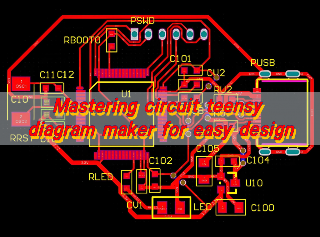
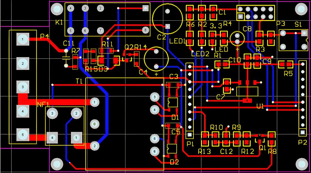
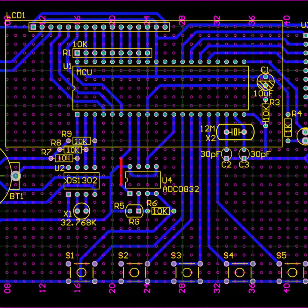
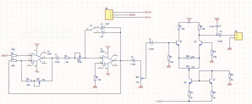
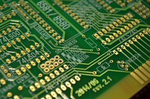
Mastering circuit teensy diagram maker for easy design, circuit diagram maker is a software or online tool. It has a rich electronic component symbol library, allowing users to place components by simple drag and drop operations, and can also use wiring tools to depict the connection relationship between components to make circuit schematics. For PCB circuit diagrams, it can reasonably layout components, set different line widths and spacing, and can also perform electrical and design rule checks, and output files in multiple formats. It is an important tool for circuit diagram production in the field of electronic design.
How do you make a simple circuit diagram?
The following are the steps to make a simple PCB circuit diagram:
1. Circuit design planning:
- Clarify the purpose and performance of the PCB, and determine parameters such as power supply voltage, current, and signal frequency.
- Select components based on function, and check the data sheet to determine the package, pins, and electrical parameters.
2. Draw a schematic:
- Select EDA software (such as Altium Designer, Eagle, KiCad, etc.) or draw it manually with pencil and graph paper (need to be converted to electronic format).
- In the software, find symbols from the component library and drag and drop them, or manually draw component symbols according to the standard and mark the names.
- Use the software to connect component pins with a wiring tool, and manually use a ruler and pencil to connect. Pay attention to the connection point representation and neat lines.
- Mark component parameters, names, packages, and network names or signal names.
3. PCB layout:
- Create a new PCB file and import schematic information.
- Determine the PCB size and shape according to requirements, such as selecting a 50mm×50mm square.
- Drag and drop components from the library into the board frame, divide them according to function, and pay attention to the spacing that is conducive to welding and heat dissipation, such as separating high-power components.
4. PCB wiring:
- Set wiring rules according to circuit properties and component parameters, such as power line width 1-2mm, signal line width 0.2-0.5mm, and spacing not less than 0.2mm.
- Manual wiring (using software wiring tools to draw lines according to connection relationships and control the direction), automatic wiring (manual adjustment after the software automatically completes) or a combination of the two.
- Check whether the wiring is compliant, whether there are short circuits or open circuits, optimize the wiring of key signals, and reduce interference.
5. Design inspection and output files:
- Use the software DRC function to check the PCB design and modify the problems according to the prompts.
- Generate Gerber files (for PCB manufacturing) and BOM files (list component information). Different software has different generation methods, such as “File”-“Fabrication Outputs” in Altium Designer to generate Gerber, and “Reports”-“Bill of Materials” to generate BOM.
What is a circuit board diagram called?
Circuit board diagrams are usually called PCB diagrams (printed circuit board diagrams). Concepts related to PCB diagrams include schematic diagrams, block diagrams, and assembly diagrams.
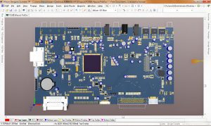
PCB diagrams are detailed layout diagrams of circuit boards, which accurately show the location of components on the circuit board and the routing of the circuit. Through the PCB diagram, you can clearly understand the location of circuit components on the PCB, the connection method, and the circuit direction, thereby ensuring the correctness and reliability of the circuit.
PCB diagrams play a vital role in the manufacturing and assembly process of electronic equipment. It guides the layout and connection of electronic components to ensure that the physical construction and assembly of the circuit are correct. The unnecessary copper foil is removed chemically or mechanically to form the path of the circuit, and then the electronic components are installed on the circuit board to form a complete circuit.
Which software is used for PCB designing?
Commonly used software for designing PCBs include Altium Designer, Cadence Allegro and Mentor Graphics PADS PCB.
1. Altium Designer
Altium Designer is a world-renowned PCB design software that supports the entire process from schematic design to PCB layout. It has a wealth of library components, powerful automatic routing functions and a variety of export functions, which can help designers complete the design quickly and efficiently.
2. Cadence Allegro
Cadence Allegro is a commercial EDA software with very rich functions. It provides control over the components and PCB software used in electronic systems to ensure the smooth implementation of the project. Allegro has a number of technologies such as three-dimensional electronic design and simulation, printed circuit board design, hardware description language, etc., which can control the workflow more finely.
3. Mentor Graphics PADS PCB
PADS PCB is a PCB design software developed by Mentor Graphics, which is widely used in communications, automobiles, medical and other fields. It provides a clear and intuitive user interface and powerful library component management functions, making the PCB design process simpler and more convenient. PADS PCB supports fully automatic routing and signal integrity analysis, effectively improving design quality and efficiency.
How do you draw a PCB layout?
1. Preparation
- Complete the schematic design and check the component connections and parameters.
- Be familiar with the component package and check the appearance, pin distribution and other information.
- Determine the PCB size and shape according to the application scenario and installation requirements.
2. Layout principles
- Place components according to functional partitions for easy debugging and maintenance.
- Arrange components according to signal flow to avoid line bending and crossing.
- Ensure component spacing and consider installation requirements.
3. Start layout
- Import the schematic information into the PCB design software.
- Place components manually and arrange them neatly using software tools.
- Adjust component positions, considering signals, routing and electromagnetic interference.
4. Check and optimize the layout
- Check whether it complies with the layout principles and design rules.
- Optimize the layout to facilitate wiring, considering multi-layer PCBs and high-frequency signals.
What does j mean on a circuit board?
The “J” on the circuit board usually stands for a socket (Connector). In circuit board design, the letter “J” is often used to represent various types of connectors or sockets for connecting different circuit boards or external devices. In addition, “J” sometimes also stands for a jumper (Jumper), which is used to temporarily connect two nodes.
What is k in a circuit diagram?
The letter “K” in a circuit diagram usually represents components such as relays and contactors. In a circuit diagram, the letter “K” can represent a variety of electrical components, including relays (KA), contactors (KM), time relays (KT), frequency relays (KF), pressure relays (KP), signal relays (KS), grounding relays (KE), etc. In addition, “K” can also represent emergency stop switches (KS).
These components play different roles in the circuit:
- Relay: used to automatically control the on and off of the circuit.
- Contactor: used to frequently connect and disconnect high-current circuits.
- Time relay: used to connect or disconnect circuits after a specific time.
- Frequency relay: used to detect and control frequency signals.
- Pressure relay: used to detect and control pressure signals.
- Signal relay: used to transmit and control signals.
- Grounding relay: used for grounding protection.
These components play an important role in circuit design and maintenance. Understanding their symbols and functions helps to better understand and maintain circuit systems.
What is the difference between a schematic diagram and a circuit diagram?
The main difference between a schematic diagram and a circuit diagram is that they focus on different focuses and usage scenarios.
1. Definition and function
- Schematic diagram: A schematic diagram is a graphical representation that is mainly used to represent the logical and functional relationship between components in an electronic device or system. It uses symbols and connecting lines to represent electronic components and signal transmission paths, without involving specific physical layouts and sizes.
- Circuit diagram: Circuit diagrams focus more on electrical connections and physical layouts, and are used to show the physical connections and relative positions between components in an electronic device or system. Circuit diagrams use symbols and connecting lines to represent electrical connections, emphasizing electrical connections and physical layout rather than just signal transmission.
2. Usage scenarios
- Schematic diagrams: Mainly used in the design and analysis stages of electronic systems. Designers use schematic diagrams to describe the logic and functions of electronic devices or systems for analysis and optimization during the design stage.
- Circuit diagrams: Mainly used in the manufacturing, maintenance and testing stages of electronic systems. Technicians use circuit diagrams to plan physical layouts and electrical connections, and visualize the structure and function of circuits before actually assembling and installing electronic devices.
3. Specific application examples
- Schematic diagrams: In the design stage, designers use schematic diagrams to describe the overall architecture and workflow of the system to ensure that the logical relationship between the components is correct.
- Circuit diagrams: In the manufacturing, maintenance and testing stages, technicians use circuit diagrams for actual circuit connections and troubleshooting.
In general, circuit teensy diagram maker is an indispensable key tool in the field of modern electronic design. Through efficient design processes, precise component layout and wiring functions, and strict rule checking mechanisms, they provide solid technical support for the research and development, manufacturing and innovation of electronic products, making complex circuit design work more efficient, accurate and reliable.


