Are you looking for copper base PCB solutions and suppliers? Let’s explore more about copper base PCB’s benefits, application and production steps, how to get a cheaper price list as well as how to select a copper based PCB factory.
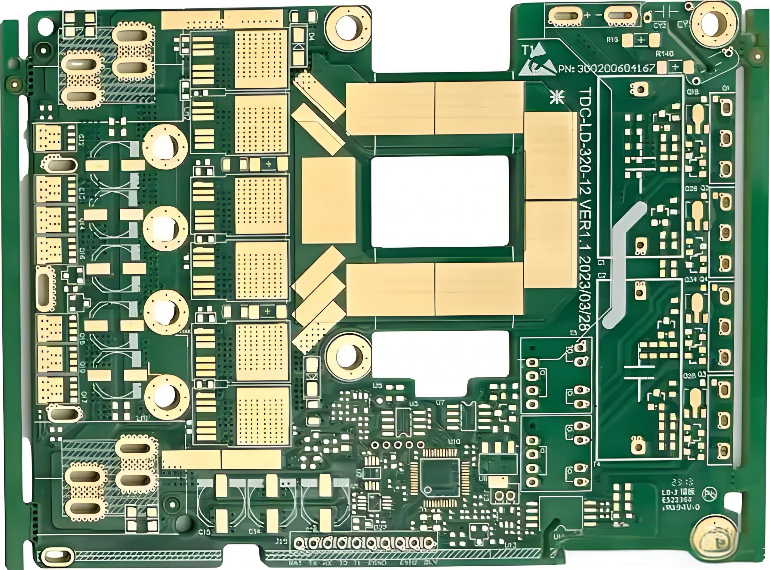
Best Technology specializes in copper base PCB manufacturing over 18 years. Our advanced manufacturing processes achieve ±0.075mm tolerance control using laser direct imaging (LDI) and automated AOI and X-Ray inspection, ensuring 99%+ production consistency. Prototype orders ship within 48 hours with full DFM analysis included, while bulk production maintains two-three weeks lead time even for complex designs. We support custom heavy copper boards up to 12 oz for high-power applications, validated through thermal cycling and HAST testing. With IATF 16949-certified workflows and dedicated engineering support for stack-up optimization, we eliminate delays from design revisions. Submit your specs today for get a solution of your case! Contact us sales@bestpcbs.com
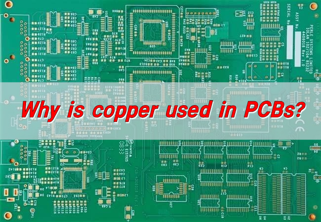
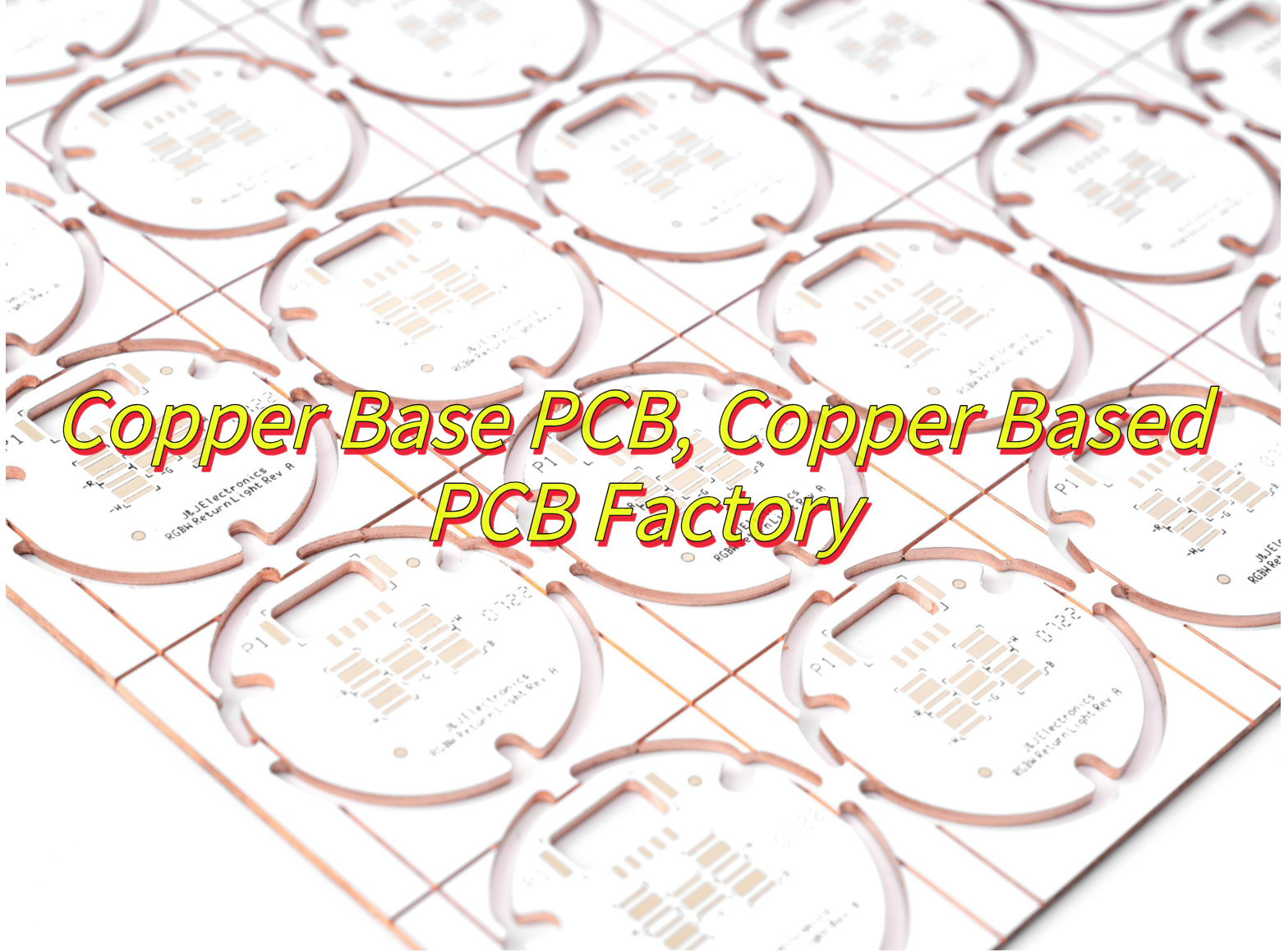
What Is Copper Base PCB?
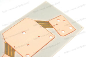
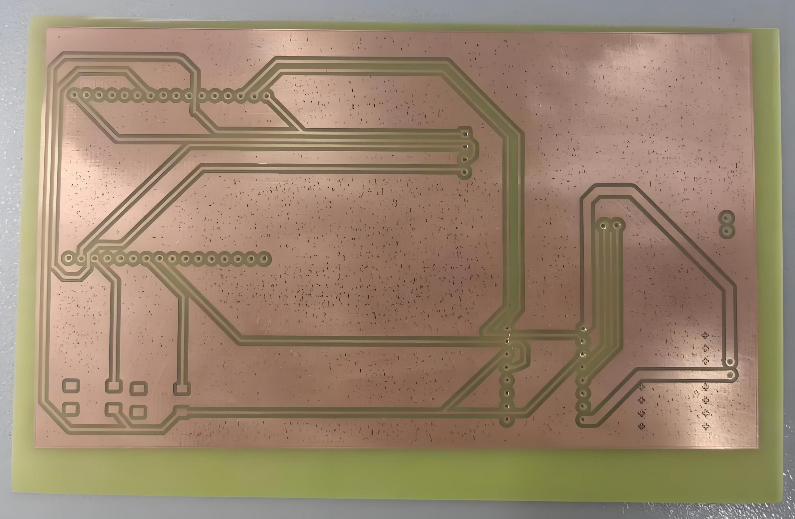
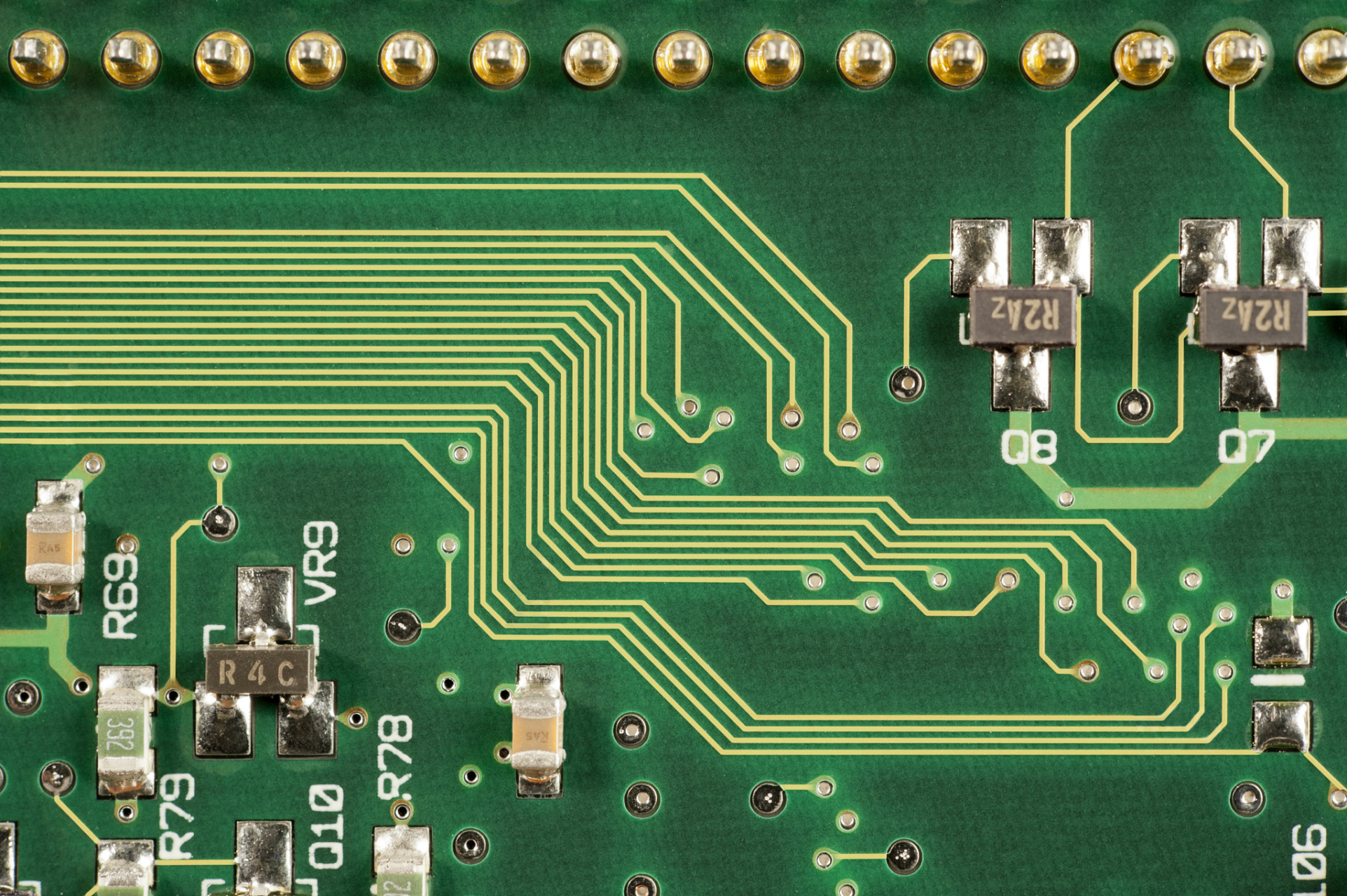
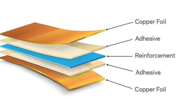
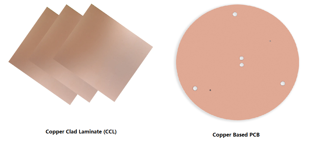
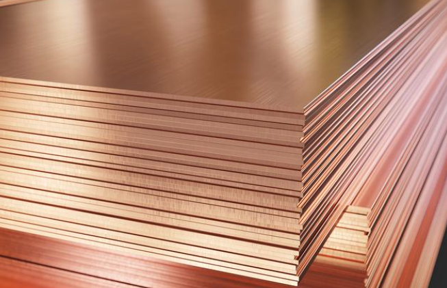
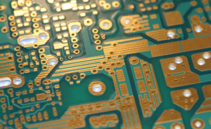
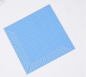
A Copper Base PCB is a metal-core circuit board engineered for high-power electronics requiring superior heat dissipation. It combines a conductive copper layer (35μm-280μm) for electrical connections, a thermally conductive dielectric layer (>400W/m·K) for insulation, and a thick copper substrate (≥1mm) to rapidly transfer heat away from components. This design outperforms aluminum-based boards in thermal efficiency and mechanical stability, making it ideal for automotive LED systems, 5G infrastructure, and industrial power modules. Its direct thermal pathway minimizes heat buildup, ensuring reliability in extreme temperatures while reducing the risk of circuit failure.
What Are Advantages of Copper Base PCBs?
Here are advantages of copper base PCBs:
- Thermal Management – Ultra-low thermal resistance + efficient heat dissipation, ideal for high-power devices (e.g., LEDs, inverters).
- Structural Stability – Excellent dimensional stability, resistant to thermal deformation, ensuring signal integrity in high-frequency circuits.
- Mechanical Performance – High mechanical strength + vibration/shock resistance, suitable for harsh environments (e.g., industrial/automotive applications).
- Non-Magnetic – No magnetic interference, ideal for precision electronics (e.g., medical/aerospace systems).
- Processing Flexibility – Superior viscoplasticity, enabling fine-line etching + platform design for enhanced heat dissipation and grounding.
- Durability – Resistant to thermal aging, ensuring long-term stable performance and reducing maintenance costs.

What Are Application of Copper Based PCB?
- LED Lighting – High-power LED systems (e.g., automotive headlights, industrial lighting) for efficient thermal management.
- Power Electronics – Core components in electric vehicles (EVs), renewable energy, and industrial automation to handle high currents and temperatures.
- Automotive Electronics – Ensures reliability in engine control units (ECUs), battery management systems (BMS), and charging infrastructure.
- Consumer Electronics – Enables compact design and thermal optimization in gaming laptops, 5G routers, and other consumer devices.
- Aerospace & Defense – Durable components in radar systems, avionics, and satellite equipment for extreme-condition environments.
- Medical Devices – Guarantees precision and thermal stability in medical imaging and diagnostic equipment.
- Telecommunications – Supports high-speed data transmission in 5G base stations, network switches, and communication devices.
- Industrial Controls – Provides stability in harsh environments for PLCs, robotics, and factory automation.
- Renewable Energy – Manages efficient power handling in solar inverters, wind turbines, and energy storage systems.
- High-Performance Computing – Addresses processor heat in servers, AI accelerators, and high-density computing.

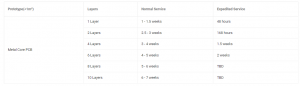
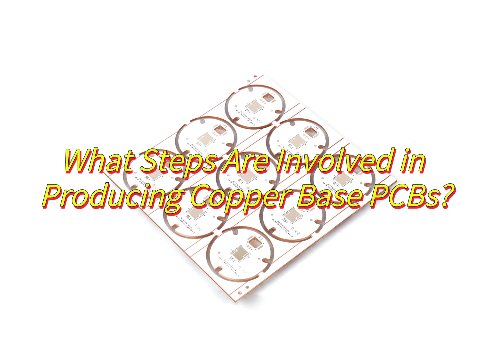
What Steps Are Involved in Producing Copper Base PCBs?
The production process of copper substrate mainly includes the following steps:
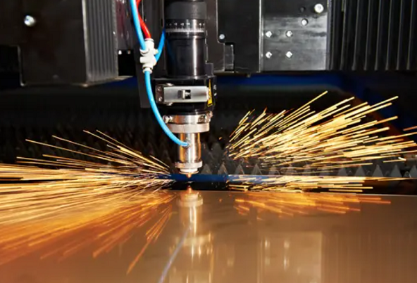
- Cutting: Cut the raw materials of copper substrate into the required size for production.
- Drilling: After positioning drilling, the copper substrate sheet is positioned and drilled to help with subsequent processing.
- Circuit imaging: Present the required part of the circuit on the copper substrate sheet.
- Etching: Keep the required part after circuit imaging and etch out the unnecessary part.
- Solder mask: Prevent non-welding points from being contaminated with solder and prevent tin from entering and causing short circuits.
- Silk screen characters: For marking.
- Surface treatment: Protect the surface of the copper substrate.
- CNC: Perform CNC operation on the entire board.
- Withstand voltage test: Test whether the circuit is working properly.
- Packaging and shipment: Confirm that the packaging is complete and beautiful, and the quantity is correct.
How to Select a Reliable Copper Base PCB Factory?
This is how to choose a trusted copper base PCB factory:
Assess Technical Capabilities
- Look for factories with advanced equipment like high-precision drilling machines, laser direct imaging (LDI) systems, and automated optical inspection (AOI) tools.
- Verify their experience in handling copper-based materials, including metal-core PCBs (MCPCBs) and thermal management solutions.
Evaluate Quality Certifications
- Prioritize factories with ISO 9001, ISO 14001, IATF 16949, and IPC-A-610 certifications. These ensure adherence to international quality and environmental standards.
Review Production Capacity & Flexibility
- Choose a factory capable of handling both small-batch prototypes and large-volume orders. Check their minimum order quantity (MOQ) and lead times.
- Ensure they can accommodate custom designs, including complex layouts and specialized thermal requirements.
Inspect Quality Control Processes
- Request details on their quality control measures, such as incoming material inspection, in-process checks, and final testing (e.g., impedance testing, thermal cycling).
- Look for factories with traceability systems to document each production step.
Analyze Supply Chain Management
- Verify their access to reliable raw material suppliers, especially for copper-clad laminates and thermal interface materials.
- Inquire about their inventory management and contingency plans for material shortages.
Consider Cost-Effectiveness
- Compare quotes from multiple factories, but prioritize value over the lowest price. Factor in costs for design support, prototyping, and post-production services.
- Ensure transparency in pricing, with clear breakdowns of material, labor, and overhead expenses.
Check Customer Support & Communication
- Evaluate their responsiveness and technical expertise. A reliable factory should offer 24/7 support and quick turnaround times for design feedback.
- Look for case studies or client testimonials highlighting their collaboration and problem-solving abilities.
Review After-Sales Services
- Ensure they provide warranties, rework services, and technical support for troubleshooting.
- Inquire about their return policies and procedures for handling defective products.
Visit the Factory (if possible)
- Conduct an on-site audit to assess their production environment, equipment maintenance, and employee skill levels.
- Observe their safety protocols and adherence to industry best practices.
Leverage Recommendations & Industry Reputation
- Seek referrals from trusted peers or industry forums. Check online reviews and ratings on platforms like Alibaba or Made-in-China.
- Look for factories with a proven track record in your specific industry (e.g., LED lighting, automotive, or power electronics).
How to Get a Cheap Quote for Copper Base PCB?
Here are some methods about how to get a cheap quote for copper base PCBs:
Optimize Your Design for Cost Efficiency
- Simplify your layout to reduce complexity (e.g., minimize via counts, avoid unnecessary layers).
- Standardize copper trace widths and spacing to align with factory capabilities, reducing production time and scrap rates.
- Use common materials (e.g., FR-4 base with standard copper thickness) instead of premium options unless thermal/electrical performance demands otherwise.
Place a Large Order Volume
- Bulk orders often qualify for tiered pricing discounts. Factories reduce per-unit costs when scaling up production.
- Consider consolidating multiple projects into a single order to meet MOQ (minimum order quantity) thresholds.
Leverage Long-Term Partnerships
- Build relationships with factories by committing to repeat business. Suppliers may offer loyalty discounts or preferential pricing.
- Negotiate volume-based contracts for recurring orders over a set period (e.g., 6–12 months).
Choose a Reliable but Cost-Effective Supplier
- Target mid-tier factories(like Best Technology) with proven quality records rather than premium brands. Research certifications (e.g., ISO 9001) to ensure reliability without overpaying for brand recognition.
Provide Clear, Actionable Specifications
- Share detailed but concise requirements (e.g., layer count, copper thickness, impedance control) to avoid rework or miscommunication.
- Use industry-standard file formats (Gerber, ODB++) to streamline quoting and production.
Avoid Frequent Design Changes
- Finalize your design before requesting quotes to prevent additional engineering fees or delays.
- If revisions are necessary, bundle them into a single update rather than incremental changes.
Consider Off-Peak Production Slots
- Inquire about factory schedules—some suppliers offer discounts for orders placed during low-demand periods.
- Flexibility on lead times may yield cost savings.
Negotiate Add-On Services Strategically
- Defer non-essential services (e.g., advanced testing, custom packaging) to reduce upfront costs.
- Bundle services (e.g., assembly + testing) with the PCB order for combined discounts.
Reduce Customization Demands
- Prioritize for standard PCB sizes, finishes (e.g., HASL vs. ENIG), and hole diameters to avoid custom tooling fees.
- Limit special requests (e.g., expedited shipping, urgent turnaround) unless critical.
Explore Regional or Local Suppliers
- If logistics allow, consider nearby factories to save on shipping and import duties.
- Regional suppliers may offer competitive pricing for smaller orders where international shipping costs are prohibitive.
What Are the Differences Between Aluminum and Copper Base PCBs?
Thermal Conductivity
- Copper Base PCB: Offers superior thermal conductivity (up to 2x higher than aluminum), making it ideal for high-heat applications like automotive lighting and power electronics.
- Aluminum Base PCB: Provides moderate thermal performance, suitable for low-to-mid-power LED lighting and general electronics where cost efficiency is prioritized.
Cost
- Copper Base PCB: More expensive due to higher material and processing costs.
- Aluminum Base PCB: Generally cheaper, making it a cost-effective choice for mass-produced consumer electronics.
Weight
- Copper Base PCB: Heavier, which may impact portability in weight-sensitive designs.
- Aluminum Base PCB: Lighter, preferred for applications requiring reduced weight (e.g., drones, portable devices).
Manufacturing Complexity
- Copper Base PCB: Requires advanced fabrication processes (e.g., metallized holes, precision etching), leading to longer lead times.
- Aluminum Base PCB: Easier to manufacture with simpler processes, enabling faster turnaround and lower setup costs.
Mechanical Strength & Durability
- Copper Base PCB: More resistant to thermal and mechanical stress, with better dimensional stability under high temperatures.
- Aluminum Base PCB: Prone to warping in extreme conditions but sufficient for standard thermal cycling in indoor environments.
Electrical Performance
- Copper Base PCB: Superior electrical conductivity and lower resistance, critical for high-frequency or high-current applications.
- Aluminum Base PCB: Adequate for basic electrical routing but may limit performance in high-speed designs.
Applications
- Copper Base PCB: Used in high-performance sectors (aerospace, automotive, industrial controls) where thermal management and reliability are paramount.
- Aluminum Base PCB: Common in consumer electronics (LED lighting, power supplies) and low-cost industrial applications.
Surface Finish & Customization
- Copper Base PCB: Supports advanced finishes (e.g., immersion gold, ENIG) for enhanced solderability and corrosion resistance.
- Aluminum Base PCB: Typically uses HASL or OSP finishes, suitable for general-purpose use but less durable in harsh environments.
Can 400 Watt Copper Base PCB Be Customized?
Yes, a 400-watt copper base PCB can be customized to suit specific requirements. Manufacturers can adjust parameters such as size, layer count, copper thickness, and thermal management solutions (e.g., choosing between aluminum or copper substrates) to optimize performance for high-power applications. Additional customization options include component placement, surface finishes (e.g., HASL, ENIG), and material choices to meet environmental or reliability standards. Many suppliers like Best Technology also offer design validation and prototyping services to ensure the custom PCB meets performance expectations before scaling to production.