pcb
Home > Blog

Posts Tagged ‘DBC ceramic PCB’

Do the vias can be filled for ceramic PCB?
Friday, November 13th, 2020

As everyone knows for FR4 PCB, people like the vias to be tented or filled for some special applications.
Ceramic PCB is more and more popular because of the thermal conductivity is very high and very good for heat dissipation. Most of customers are going to make the PCB with ceramic material, includes Al2O3, AlN, BeO or Si3N4, etc.
So do the vias can be filled for ceramic PCB becomes the frequently asked questions (FAQ).
The answer is YES.
So what’s the material can be filled in vias for DBC/DPC alumina PCB/ Aluminium Nitride PCB?

The material can be solder mask, Dow Corning 1-4173 and copper/Cu.
Normally, customers want the vias/holes to be filled with copper.
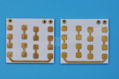
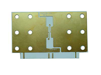
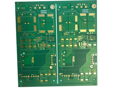
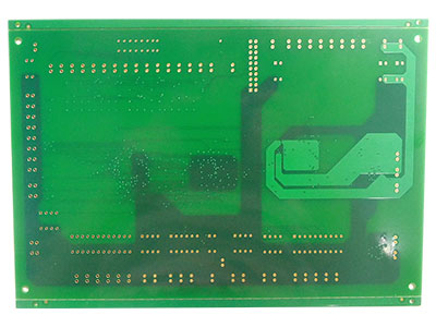
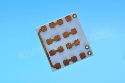
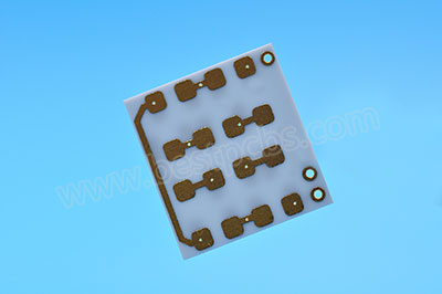
Because copper can fill the vias very well and it is easier to do and it looks very good. Please see below photo.
The left one with filling with copper, the right one without filling copper
Why you need to fill the vias with copper?
1.Becuase if let the vias open, they will allow solder to flow through to opposite side of PCB during reflow, this causes bridging under components.
Filling the open vias/holes with copper can prevent from the solder pates into the vias.
2.If you need to pull vacuum around them and a hole would compromise that, so need to fill the vias.
There are also other purposes for filling the vias, if you need such ceramic board with filling the vias, please contact Coco in Best Technology sales@bestpcbs.com

You may also like

Why don’t use BeO as substrate to make DBC ceramic PCB?
Wednesday, September 9th, 2020

It is widely known that BeO with high thermal conductivity (200-250W/m.k).

High dielectric constant 6-7 (0.1MHz) and dielectric loss tangent is 10-4 (0.1GHz).

It is ideal material for ceramic PCB, lots of engineers want to use it as DBC ceramic PCB substrate.

But it is unfeasible, the powder of BeO is extremely poisonous.

The poison gas is produced by the reaction between oxygen, Cu and BeO under

1065-1085 degrees Celsius, so it is limited to make cooper on BeO substrate,

it has caused AlN (Aluminium Nitride) is becoming more and more popular.

Though BeO is unfeasible for DBC technology, but it is feasible for thick film technology.

Because when doing the conductor (Au or AgPd) on BeO substrate, we use silk-screen printing, no need to under high temperature environment, there is no chemical reactions.

Below the manufacturing process for your reference.

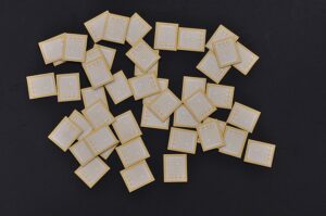
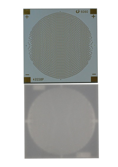
Here is the photo of BeO with AgPd conductor.

You may also like

What’s the advantages for AMB ceramic PCB comparing with DPC, DCB, LTCC, HTCC, thick film ceramic PCB?
Tuesday, August 18th, 2020

As we know, there are all kinds of ceramic PCB, DPC ceramic PCB, DBC ceramic PCB, LTCC ceramic PCB, HTCC ceramic PCB, thick film/thin film ceramic PCB.

Very few people know that there is AMB (Active Metal Bonding) ceramic PCB.

Do you know what’s the advantage for AMB ceramic PCB compare with other ceramic PCB (Al2O3/AlN/BeO/Si3N4 PCB)?

For AMB PCB, the substrate can be AlN ( Aluminium Nitride) and Si3N4 (Silicon Nitride) normally, AlN is the most popular. It is widely known that AlN with very high thermal conductivity ( Theoretical Value is 320W/m.k).

Using AMB technology to combine the oxygen-free copper and AlN material under high temperature, AlN with smaller thermal resistance, lower coefficient of thermal expansion and more stable partial discharge capability.

Compared with the traditional DBC or other substrate, the Aluminum Nitride copper-clad ceramic substrate made by the AMB technology with higher bonding strength of the copper layer and better cold and hot cycling characteristics.

So it  is widely used in the field of IGBT, especially for the high-power device control module.

AMB with competitive price and the copper thickness can be much thicker.

AlN max 300um
Si3N4 max 1200um

For more details, please contact me sales@bestpcbs.com 
I will update the manufacture process at the end of this month.

You may also like

Why don’t use BeO as substrate to make DBC ceramic PCB?
Monday, June 22nd, 2020

It is widely known that BeO with high thermal conductivity (200-250W/m.k). High dielectric constant 6-7 (0.1MHz) and dielectric loss tangent is 10-4 (0.1GHz), extremely high working temprature. It is ideal material for ceramic PCB, lots of engineers want to use it as DBC ceramic PCB substrate.

But it is not popular in ceramic PCB market, comparing with Al2O3, AIN, Si3N4, or ZrO2, as the powder of BeO is extremely poisonous.

The poison gas is produced by the reaction between oxygen, Cu and BeO under 1065-1085 degrees Celsius, so it is limited to make cooper on BeO substrate, it has caused ALN (Aluminium Nitride) is becoming more and more popular.

Right now, only few countries are using BeO to make ceramic PCB, such as USA, Russia and China. USA had biggest capability to make BeO , and here in China, there’re still some companies to make BeO raw material and among them, a few companies to produce direct copper bonded (DCB) on BeO because of environment limitation.

Though BeO is not popular for DBC technology, but it is feasible for thick film technology, because when the mentalization of Ceramic PCB, the conductor (Au or AgPd) on BeO substrate was made by silk-screen printing, and drying temperature is only around 850C, no need to under high temperature environment, so there is no chemical reactions, no environment issue.

Below the thick film ceramic PCB manufacturing process for your reference.

https://www.bestpcbs.com/products/thick-film-ceramic-pcb-manufacturing-process.htm

Here is the photo of BeO with AgPd conductor.

BeO with AgPd conductor

Welcome to contact us if you have better idea, or different comments on BeO ceramic PCB, communation will make us becoming better and better.

You may also like