

There are many differences between single sided and double sided PCB in terms of structure, performance, application scenarios, etc. Single-sided PCB has conductive lines on only one side, while double-sided PCB has conductive lines on both sides, which makes them perform differently in terms of the complexity of circuit layout, signal transmission capability, and the types of electronic devices they are suitable for.
What is the difference between single and double sided PCB?
The main difference between single-sided PCB and double-sided PCB lies in their structure and use. Single-sided PCB has only one layer of lines, which is suitable for simple circuits; while double-sided PCB has two layers of lines, which is suitable for complex circuits.
The characteristics and application scope of single-sided PCB are as follows:
- 1. Structure: Single-sided PCB has only one layer of lines, and all components are on the same layer and connected by copper foil lines.
- 2. Application scope: Usually used for simple circuits, such as LED lights, alarm clocks, etc.
- 3. Advantages: Low manufacturing cost and simple manufacturing process.
- 4. Disadvantages: Only simple circuit layout can be realized, and the crossing of lines will increase the size of the board, which is not suitable for complex circuit layout.
The characteristics and application scope of double-sided PCB are as follows:
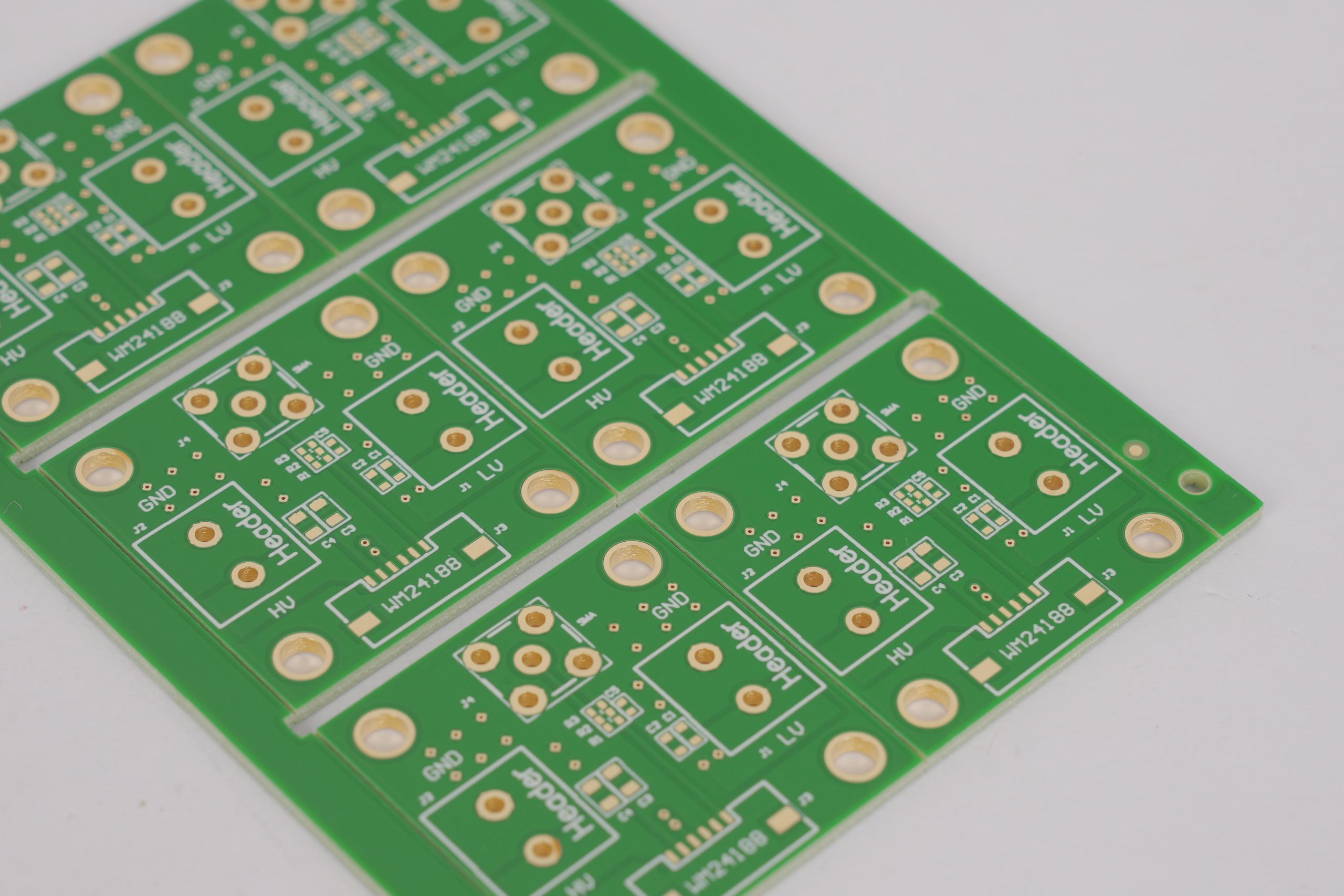
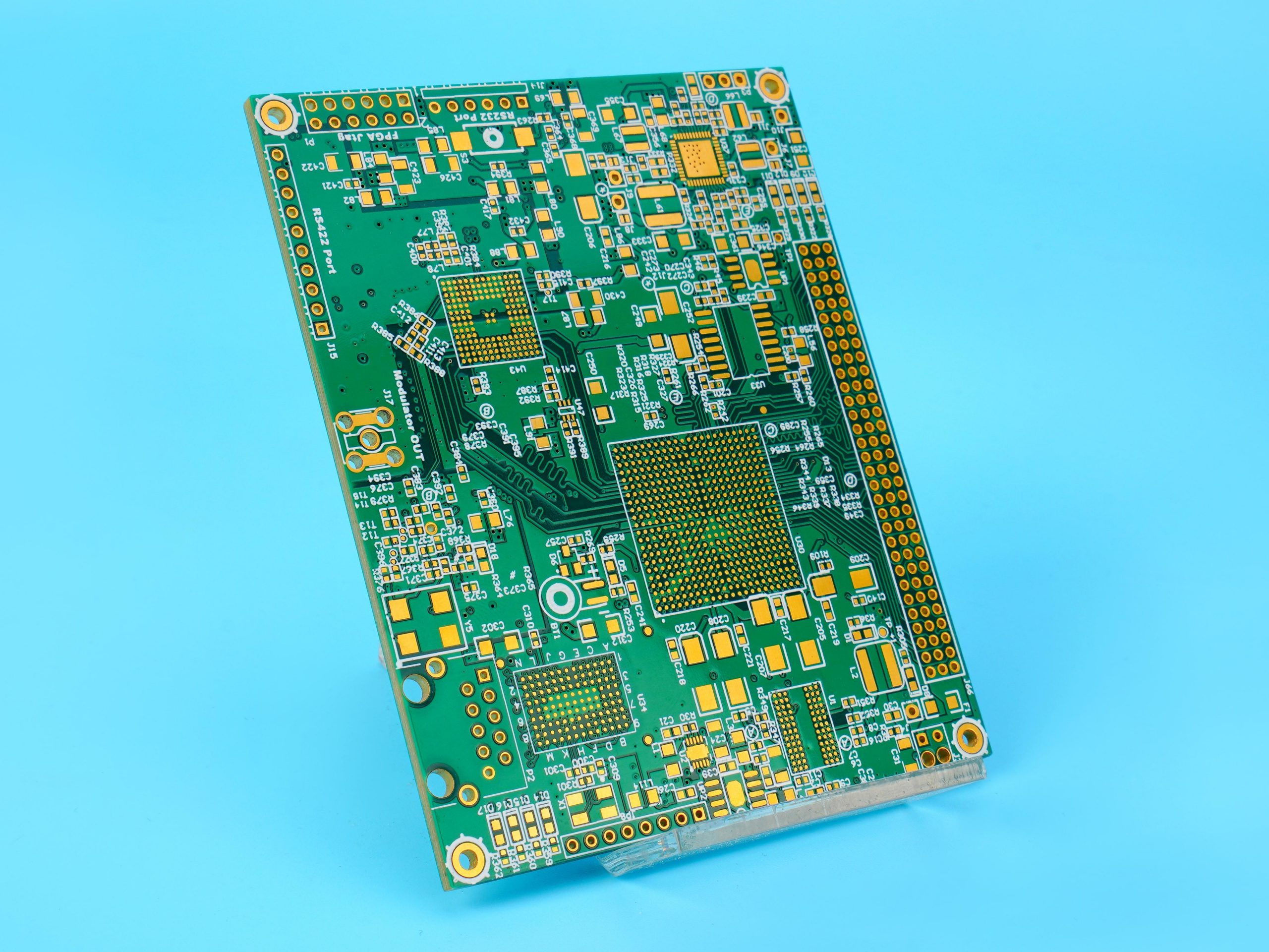
- 1. Structure: Double-sided PCB has two layers of lines, and components can be arranged and connected on two levels, and connected to each other through jacks and pads.
- 2. Application scope: Usually used for complex circuits, such as computers, mobile phones, etc.
- 3. Advantages: Complex circuit layout can be realized, and the crossing of lines will reduce the size of the board.
- 4. Disadvantages: The manufacturing cost is high, and the manufacturing process is more complicated than that of single-sided PCB, which is not suitable for ultra-large circuit layout.
The differences in materials and processes between single-sided PCB and double-sided PCB are as follows:
- 1. Material: Single-sided board has copper foil on only one side, while double-sided board has copper foil on both sides.
- 2. Process: The solder joints of single-sided board are basically on one side, and components are inserted on the other side; both sides of double-sided board can be soldered, with plug-in components and SMD components.
Why use single sided PCB?
Single-sided PCB is mainly used for simple circuit design and cost-sensitive applications. Since there is only one side of the single-sided board with wiring, the wiring is difficult, so it is mainly suitable for simple circuit design.
The advantages of single-sided PCB include low cost and relatively simple manufacturing process. Since the manufacturing process of single-sided board is relatively simple and does not require complex multi-layer wiring and connection, the cost is low and suitable for mass production.
What is the advantage of single layer PCB?
The main advantages of single-layer PCB include:
- 1. Low cost: The manufacturing cost of single-layer PCB board is relatively low, because only one layer of copper foil and one layer of substrate are required, the manufacturing process is relatively simple, and the material cost is low.
- 2. Easy to make: Compared with other structural types of PCB boards, the manufacturing method of single-layer PCB board is relatively simple, only single-sided wiring and single-layer corrosion are required, the manufacturing difficulty is low, the drilling, welding and installation of components are relatively simple, and it is unlikely to cause production problems.
- 3. High reliability: Single-layer PCB board does not have multi-layer wiring and connection, so it is not easy to have problems such as short circuit and interference, and has high reliability.
- 4. Suitable for simple circuits: Single-layer PCBs are suitable for simple circuit designs, such as LED lights, household appliances, etc., and can meet most low-complexity circuit requirements.
What are the disadvantages of single sided PCB?
First, the difficulty of wiring a single-sided PCB is a significant disadvantage. Since there is only one layer of copper foil, wiring is difficult, and the layout of the circuit and the location of components need to be carefully planned to avoid short circuits or circuit failures caused by improper wiring.
Second, the electromagnetic interference suppression capability of single-sided PCBs is relatively poor. In high-frequency circuits, the electromagnetic interference problem of single-sided PCBs will be more prominent and become an important factor to be considered during design.
Finally, single-sided PCBs limit the complexity of the circuit. Since it has only one layer of copper, it is not suitable for the design of complex circuits. For circuits that require high complexity, double-sided or multi-layer PCBs would be a better choice.
What are the advantages of double sided PCB?
The main advantages of double-sided PCBs include:
- 1. Enhanced circuit density: The available surface area of double-sided PCBs is doubled, and more components can be attached.
- 2. Higher signal transmission rate: Double-sided PCB design makes the circuit more complex and flexible, thereby improving the signal transmission rate and circuit performance.
- 3. More reliable circuit connection: By passing the circuit through holes between the two sides, the circuit can be connected on both sides, greatly improving the density and reliability of the circuit board.
- 4. Convenient wiring and debugging: The design of double-sided PCB makes wiring more flexible, convenient for complex circuit design, and also convenient for subsequent debugging and maintenance.
- 5. Environmental protection and high efficiency: Double-sided PCBs are made of non-toxic and pollution-free materials, which meet environmental protection requirements, and can carry more electronic components and improve the working efficiency of equipment.
Where are double sided PCBs used?
The characteristic of double-sided PCBs is that both sides can be wired and assembled with electronic components, and the lines on both sides are connected through holes (vias), so as to achieve more complex circuit design.
This design makes double-sided PCBs perform well in application scenarios that require high-density assembly and complex circuit layout. Due to the presence of vias, double-sided PCBs can achieve more complex circuit designs without significantly increasing the size of the circuit board.
Specific application areas include:
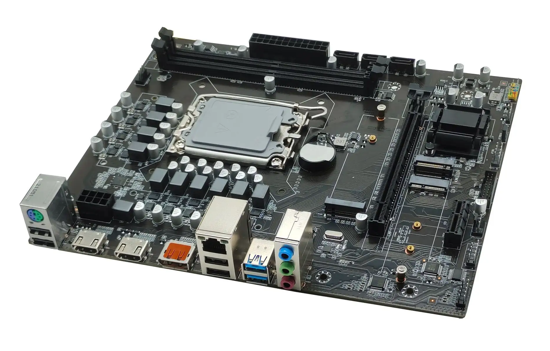
- 1. Computer and industrial control: Double-sided PCBs are widely used in computer motherboards and industrial control systems, providing complex circuit designs and high-density component layouts.
- 2. Communication equipment: In communication equipment, double-sided PCBs are used to achieve high-density signal processing and transmission, supporting various communication protocols.
- 3. Consumer electronics: In devices such as smartphones, tablets, routers, etc., double-sided PCBs are used to achieve complex circuit functions and efficient space utilization.
- 4. Aerospace: In the high-tech field, double-sided PCBs are used for applications with high performance requirements and strict space constraints.
What are the two sides of a PCB called?
The two sides of a PCB are called the top layer and the bottom layer.
The top layer is usually used to place and layout electronic components such as chips, resistors, capacitors, etc. The pins, wires, identifiers, and markings of the components can be seen on this layer. The top layer is also called the component side.
The bottom layer is mainly used to connect the pins of electronic components and connect to the top layer through appropriate wires. In this layer, you can see the pads, vias, connections, and possible ground and power planes. The bottom layer is also called the solder side.
In addition to the top and bottom layers, PCBs may also contain other layers, such as signal layers, power/ground layers, mechanical layers, solder mask layers, solder paste protection layers, and no-routing layers. These layers play different roles in PCB design, such as providing circuit routing, mechanical support, and preventing short circuits.
Can you put components on both sides of a PCB?
Components can be placed on both sides of a PCB. The design of double-sided PCBs allows components and wiring to be placed on both sides of the circuit board, thereby increasing the complexity and functionality of the circuit.
Design features of double-sided PCBs include:
- Dual use of wiring and components: Both sides of a double-sided PCB can be used for wiring and component placement, which greatly increases the complexity and functionality of the circuit.
- Via connection: In order to achieve interconnection between components and wiring on a double-sided PCB, connections need to be made through vias. A via is a small hole filled or coated with metal that connects wires on both sides.
The use scenarios of double-sided PCBs include:
- Increasing circuit density and functionality: Double-sided PCBs increase the layout space for components, allowing designers to achieve more functions without increasing the size of the circuit board, which is particularly suitable for occasions that require high-density integration and complex circuit design.
In short, single-sided and double-sided PCBs differ significantly in many aspects. Both single-sided and double-sided PCBs contribute to the vigorous development of the electronics industry and continue to help electronic technology move forward. BEST Technology has abundant upstream and downstream resources for circuit boards, and can quickly and efficiently meet customers’ various needs for circuit boards.