What Is Direct Thermal Path Copper PCB?
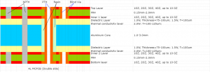
A Direct Thermal Path Copper PCB, also called DTP copper PCB or sinkpad copper base PCB. It is a type of high-performance circuit board used in applications where heat dissipation is critical. Unlike standard printed circuit boards (PCBs), which rely on dielectric layers to insulate the copper circuitry from the metal base, a DTP PCB removes this insulation layer directly beneath the heat-generating components. This creates a direct connection between the component, the copper layer, and the copper base.
This structure allows heat to flow quickly and efficiently away from the source, reducing thermal resistance and improving the performance and reliability of electronic components, especially in high-power or high-current environments. These boards are widely used in LED lighting, automotive systems, telecom infrastructure, and power electronics.

Why Thermal Management Matters in Electronics?
Every electronic device generates heat when it’s running. While small gadgets like phones may only get warm, high-power devices like industrial lighting systems or motor controllers can heat up rapidly. If this heat isn’t removed effectively, it can cause serious problems:
- Component failure
- Reduced lifespan of electronic parts
- Malfunction due to overheating
- Safety risks, especially in automotive or aerospace applications
To prevent these outcomes, thermal management becomes a critical aspect of PCB design. Engineers use a combination of heat sinks, thermal vias, and copper planes—but in extreme conditions, these are often not enough. That’s where DTP copper PCBs come in—they allow maximum heat transfer from hot components to the surrounding environment, helping electronics run cooler and more reliably.
Features of DTP Copper PCB
Direct thermal path copper PCBs stand out due to their special construction and capabilities. Here are some of their key features:
- Thick copper base (up to 10 oz or more): Helps carry more current and draw heat away quickly.
- Direct contact between copper circuit and metal base: Eliminates the thermal barrier of dielectric materials.
- Excellent heat dissipation: Thermal resistance is significantly lower compared to regular MCPCBs.
- Strong mechanical structure: Supports heavy components without deformation or cracking.
- Stable performance in harsh environments: Suitable for high-temperature, vibration, and high-voltage conditions.
These features make DTP PCBs a practical choice for demanding applications where standard PCBs would overheat or fail.
How Does DTP PCB Work?
The principle behind a DTP PCB is simple: remove the thermal barrier (dielectric layer) between the heat source and the metal base. In a typical metal core PCB, the heat generated by a component passes through a dielectric layer (which is an electrical insulator) before reaching the metal base. This dielectric slows down the heat transfer.
In a DTP PCB, the designer removes the dielectric material under the power component and creates a direct copper pad that touches the metal base directly. This structure dramatically reduces thermal resistance and allows heat to flow out much faster.
In short, DTP PCBs give heat a shortcut—a direct path to escape—leading to lower operating temperatures and better performance.
How Does the Convexity Pad Create?
The convexity pad is a small bump or raised copper structure that connects the top copper circuitry directly to the metal base below. This feature is critical in DTP PCBs because it serves as the contact point for heat transfer. Actually, the convexity pad is a little complicated than normal. Normally the thickness of copper core/substrate is 0.8mm, 1.0mm, 1.2mm, 1.4mm, 1.6mm, 2.0mm. And there’re blue protection film on both sides. We will remove that protection film after raw material cutting, before convexity making, so that copper can be etched. After that, we will grind the copper core to make sure it’ll be clear enough, so that in next step another film can be added to make trace.
Then, we will add one extra layer of film (normally blue color, and will refer to blue film hereafter) on whole area copper core, and after developing & etching, only selected area of blue film will be kept and other area will be removed away. In fact, the area of blue film will be the place convexity will be.

Why Aluminum Base Is Not Suitable to Make DTP PCB?
As we know, the convexity pad directly connects the copper base serving as the substrate to the thermal pads of the LED without any insulating thermal conductive material in between. In this way, the heat from the LED can be directly transferred to the copper substrate of the base through the solder, without having to pass through the electrical traces on the base surface and the insulating materials for heat transfer. This is why DTP PCB also is called thermoelectric isolation as well. (The heat output path of the LED is directly connected to the copper plate and separated from the electrical traces). As for why aluminum substrates cannot be used, it is because the heat pads of the led chips need to be directly soldered to the copper substrate through the solder on the reserved protrusion on the base, and aluminum doesn’t bond well with standard solder materials.
In addition to this, some manufacturers said they can make DTP aluminum PCB. Maybe they indeed made it, but need to spend a lot of time and the cost is much higher than DTP copper base PCB. And compared with copper base PCB, the thermal conductivity of aluminum PCB is slightly lower, so we always not recommend customers to make DTP aluminum PCB.
Considerations While Using Direct Thermal Path MCPCB
Before incorporating DTP copper PCBs into your design, keep these factors in mind:
1. Component Placement
Ensure components that generate high heat are directly above the DTP pads. Misalignment can compromise thermal efficiency.
2. Base Thickness
The thickness of the copper base affects both heat transfer and mechanical strength. Heavier bases improve heat conduction but may reduce flexibility.
3. Thermal Simulation
Use thermal analysis software to simulate heat dissipation before production. This helps identify hotspots and optimize layout.
4. Dielectric Material
Where dielectric is still used, choose materials with high thermal conductivity (such as ceramic-filled polymers).
5. Mounting & Enclosure
DTP PCBs perform best when mounted to a heatsink or metal enclosure. Make sure there’s good thermal interface material between them.
6. Surface Finish
Use finishes like ENIG (Electroless Nickel Immersion Gold) or OSP (Organic Solderability Preservative) to improve soldering and surface protection.

DTP Copper PCB Manufacturing Process
Manufacturing a direct thermal path copper PCB requires careful attention and precision. Here’s a step-by-step breakdown:
Step 1: Base Metal Selection
A thick copper base (typically 1.6–3.2 mm) is chosen as the base layer. This base serves as the thermal sink for the entire board.
Step 2: Lamination
A high-thermal conductivity dielectric is laminated to the copper base. This is done only where insulation is needed.
Step 3: Circuit Layer Preparation
A copper foil (typically 1–3 oz) is applied on top. The PCB manufacturer then performs photolithography and etching to define the circuit pattern.
Step 4: Dielectric Removal
The dielectric under high-heat components is selectively milled or punched to expose the copper base.
Step 5: Convex Pad Formation
Using precision CNC machining, a raised copper pad is formed on the exposed area. This pad directly contacts the component’s thermal pad.
Step 6: Surface Finishing
The board receives a protective finish like ENIG, OSP, or immersion silver to prevent oxidation and improve solderability.
Step 7: Solder Mask and Silkscreen
Solder mask is applied to protect the circuitry, followed by silkscreen for labeling.
Step 8: Testing and Quality Control
Each board undergoes electrical and thermal testing to ensure performance, conductivity, and durability.
This manufacturing process results in a high-performance PCB that can handle extreme heat conditions with ease.
Common Applications of DTP MCPCB
Because of their outstanding heat management, DTP copper PCBs are widely used across industries that rely on high-power or high-brightness components. Here are some key applications:
- Automotive LED lighting: Headlights, brake lights, and DRLs require efficient thermal dissipation to maintain brightness and longevity.
- Power electronics: DTP PCBs are used in DC/DC converters, motor controllers, and battery management systems for better heat control.
- Industrial lighting: High bay and floodlights benefit from improved thermal design to prevent premature failure.
- Telecommunication systems: Base stations and network equipment use DTP PCBs to manage heat from amplifiers and processors.
- Aerospace and defense: Systems in satellites and aircraft need PCBs that perform reliably under thermal and environmental stress.
Wherever performance and reliability are non-negotiable, DTP copper PCBs are a trusted solution.
FAQs About Direct Thermal Path MCPCB
Q1. What makes DTP PCBs different from regular MCPCBs?
The key difference is the removal of the dielectric layer beneath the component, enabling direct heat flow from the copper pad to the metal base. This dramatically improves thermal conductivity.
Q2. Can DTP copper PCBs be used in multilayer stackups?
Typically, they are single-sided. However, hybrid multilayer configurations are possible for complex applications, though they require advanced design and manufacturing techniques.
Q3. Is copper the only metal used for DTP base material?
In high-end applications, copper is the preferred base due to its superior conductivity and durability. Aluminum is cheaper but less effective in DTP designs.
Q4. Do I still need a heatsink with a DTP PCB?
Yes, in most cases. While the DTP board efficiently moves heat to its base, the heat still needs to exit the board—often through a heatsink or the product’s metal housing.
Q5. How can I get a DTP copper PCB made?
You’ll need a PCB manufacturer like Best Technology that specializes in metal core PCBs and has equipment for precision CNC milling and selective dielectric removal. Request thermal simulation support for best results.


