In the PCB design and testing, there is a common term be mentioned frequently, that is EMI and EMC. Some people may ask that “what is EMI/EMC, why is it be mentioned every time?” Today, BEST team will take you to understand what are they and how to test them. Let’s keep reading.
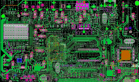
What are EMI and EMC in PCB?
Before diving into, we should know both EMI and EMC are important elements during the PCB design. Some new PCB projects are failed during testing, because EMI and EMC design is not reasonable.
EMC is short for electromagnetic compatibility. EMC in a PCB is the ability of the PCB to operate in its electromagnetic environment without creating unbearable electromagnetic interference to other devices around it. In general, to achieve an EMC compliant design, engineers need to consider three basic aspects:
- Generating unwanted electromagnetic radiation and its propagation.
- The vulnerability of designs or components to electromagnetic interference (EMI).
- PCB design should not cause intolerable electromagnetic interference on its own.
EMI is short for electromagnetic interference. EMI is unwanted noise or signals generated by electronic devices, which can disrupt other nearby equipment. PCBs, being central to electronics, are often both sources and victims of EMI. Every engineer should follow EMC configuration standards to minimize the total amount of EMI and its impact.
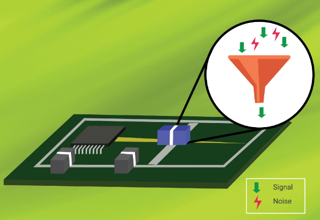
In a word, EMI refers to the generation of electromagnetic interference, while EMC refers to electromagnetic compatibility, that is, how well a device blocks EMI. EMI originates from electromagnetic equipment, and EMC involves equipment that is both anti-interference and non-interference with other equipment.
What Is the Difference Between EMI and EMC Testing?
EMI testing focuses on measuring the interference a device generates. It aims to ensure that the PCB doesn’t emit electromagnetic waves that can interfere with other devices. EMC testing, on the other hand, checks the device’s ability to withstand electromagnetic interference from its environment without losing functionality. Both tests are essential to make sure that your PCB not only works well but also doesn’t cause problems for other systems.
The main difference between EMC tests and EMI is their purpose and method of testing.
Test purpose
- EMC testing focus on the equipment or system will function properly in an electromagnetic environment and will not cause intolerable electromagnetic disturbance to other equipment. EMC testing includes two aspects: electromagnetic immunity (the ability to resist interference) and electromagnetic emission (not to interfere with other equipment).
- However, EMI testing focuses on unwanted electromagnetic energy emitted by a device or system that may interfere with the normal operation of other nearby equipment. The purpose of EMI testing is to identify and reduce these sources of interference to prevent interference with other equipment
Testing method
- EMC test usually includes shielding, grounding, and filtering methods. Shielding is surrounding devices or systems by using conductive materials to reduce leakage of electromagnetic radiation. Grounding is connecting the metal housing and ground to provide a safe electrical circuit loop. Filtering is to reduce unnecessary electromagnetic signal transmission through PCB circuit design.
- EMI test mainly measuring by the conducted interference and radiation interference of the devices. Conducted interference is interference that travels through a conductive medium (such as a wire), while radiative interference refers to the interference that travels through space.
What Are the Testing Standards for EMI/EMC?
Several global standards guide the EMI/EMC testing process. These include:
IEC 61000 series: This is the most common EMC test standard, covering EMI and EMS (Electromagnetic sensitivity) test methods, limits and units of measure.
EN 55014 series: This is the EU EMC test standard, including:
EN 55014-1: Radiation from household appliances
EN 55014-2: Radiation immunity of household appliances
EN 55032 : Interference emission test for multimedia electronic products
EN 55035 : Immune immunity test for multimedia electronic products
GB/T17625 series : This is China’s EMC test standard, including:
GB/T17625.1-2012 : EMC limits Harmonic current emission limits (Input current per phase ≤16A)
GB/T17625.2-2007 : Limits on voltage variation, voltage fluctuation, and flicker (rated current of equipment per phase ≤16A)
GB/T17625.7-2013 : Harmonic current limit for conditionally connected devices with rated current ≤75A in a common low-voltage power supply system
GB/T17625.8-2015 : Harmonic current limit for devices connected to a common low-voltage system with input current greater than 16A but less than 75A per phase
GB/T17625.9-2016 : Signal transmission emission levels, frequency bands and electromagnetic disturbance levels on low-voltage electrical installations
GBZ17625.3-2000 : Limits on voltage fluctuations and flickers in low-voltage supply systems for devices with rated current >16A
GBZ17625.6-2003 : Limits on harmonic currents produced by devices with rated current >16A in low-voltage power supply systems
GBZ17625.13-2020 : Evaluation of emission limits for unbalanced installations connected to medium voltage, high voltage, and ultra-high voltage power systems
GBZ17625.14-2017 : Evaluation of emission limits for harmonics, interharmonics, voltage fluctuations and unbalance of nuisance devices connected to low voltage power systems
GBZ17625.15-2017 : Evaluation of low frequency electromagnetic immunity and emission requirements for distributed generation systems in low voltage power grids
These standards cover a wide range from household appliances to industrial equipment, you can follow one of them according to your specific applications and countries.
How to Conduct an EMI Test?
Before conduct a test, let’s know the testing method. EMI test methods mainly include the following :
1. Pre-test: EMI testing performed during the design phase to detect and resolve EMI problems early in product design and development. Pre-test can be conducted using computer simulation, or by using actual test equipment.
2. Emission test: It is a test to measure whether electromagnetic waves emitted by equipment meet EMI standards. The emission test can be carried out by field test, half-time test, full-field test and other methods. Commonly used test equipment includes spectrum analyzer, scanning receiver, antenna, etc.
3. Sensitivity test: Common sensitivity testing methods include radiation sensitivity testing and conduction sensitivity testing. radiation sensitivity testing uses a signal generator to generate an electromagnetic field of a specific frequency and intensity. And conduction sensitivity testing involves injecting simulated electromagnetic interference signals on the power or signal lines of the equipment under test.
4. Spectrum analysis: By measuring the spectrum of electromagnetic wave to analyze the characteristics of electromagnetic interference.
Above are the testing methods of EMI, and here is the steps that how to test it.
- Select the right test method
First of all, select a right test method according to the specific test purpose and object. For example, if the emission characteristics of the equipment need to be evaluated, an emission test can be selected; If you need to evaluate the anti-interference capability of the equipment, you can choose sensitivity test.
- Use professional equipment
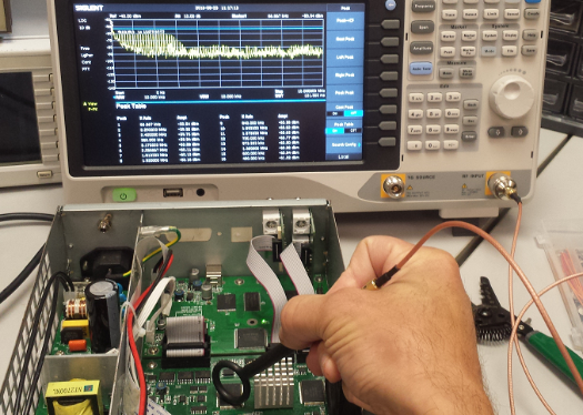
Use professional test equipment, such as spectrum analyzer, signal generator, digital storage oscilloscope, etc., to ensure the accuracy of the test results.
- Environment control
When performing sensitivity test, control the test environment to avoid the influence of other electromagnetic interference sources. Tests can be conducted in a shielded room to reduce outside interference.
- Data analysis
Detailed analysis of the test data, identify potential sources of electromagnetic interference, and propose improvement measures. Methods such as difference method and potential zeroing method can be used to reduce the influence of interfering magnetic field on measurement results.
EMI/EMC PCB Design Guidelines
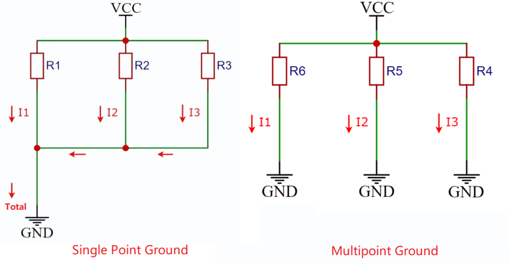
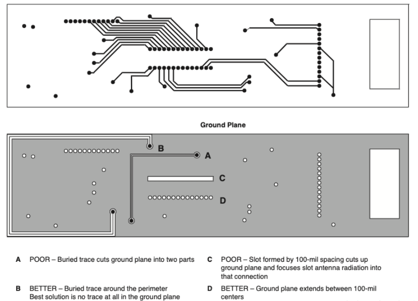
1. Ground plane
Because all circuits need to be grounded, the ground plane is the first line of defense against EMI. The following measures can be taken to reduce EMI:
- Increase the ground area
- Set up the ground plane
- Each component should be connected to the ground plane
- Each component should be connected to the ground plane or a ground point.
- Decoupling capacitor
- The ground plane is placed directly below the plane with the signal trace
- Digital ground and analog ground should be separated
- The ground wire should be as thick as possible
- The length of the ground system should be kept to a minimum
2. Power supply design
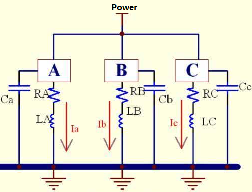
Improper power supply design will result in greater noise and ultimately reduce product performance. Two main factors that lead to power supply instability:
1) Excessive transient AC current under high-speed switching
2) Inductance exists in the current loop Therefore, the integrity of the power supply should be fully considered in PCB design.
3. PCB layout
a) PCB size
PCB size must be considered. When it comes to oversized boards, the traces must go a long way as the impedance increases, the noise immunity decreases, and the manufacturing cost increases. When the board size is particularly small, it will cause heat dissipation problems and crosstalk is prone to occur between adjacent traces. The recommended PCB size is a rectangle with an aspect ratio of 3:2 or 4:3. In addition, when the board size exceeds 200mm*150mm, the mechanical strength of the board retraction should be considered.
b) Avoid right angles
This has been said many times. Avoid 45° to 90° for vias, traces, etc. When the trace reaches more than 45°, the capacitance will increase.
c) Keep signals separated
Digital circuits, analog circuits, and noise sources should be placed independently on the board, and high-frequency circuits should be isolated from low-frequency circuits. In addition, attention should be paid to the component distribution of strong and weak signals and the direction of signal transmission.
d) Increase the trace width as much as possible
e) Wider trace sizes can effectively reduce radiated emissions.
f) Make the return current path as short as possible and route along the path with the least resistance. The length of the return path should be roughly the same as or shorter than the length of the transmission trace.
4. Component placement
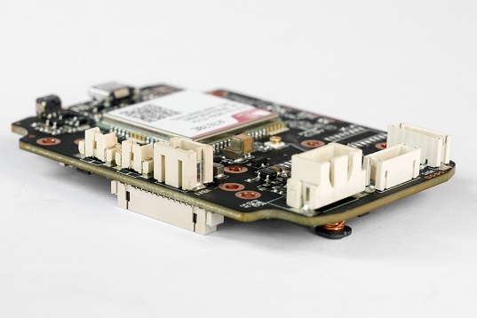
In general, it is best to completely separate analog and digital signals. Being too close can easily lead to problems such as crosstalk. In addition, compatible components should be placed independently to ensure that components do not interfere with each other in space.
5. PCB layer design
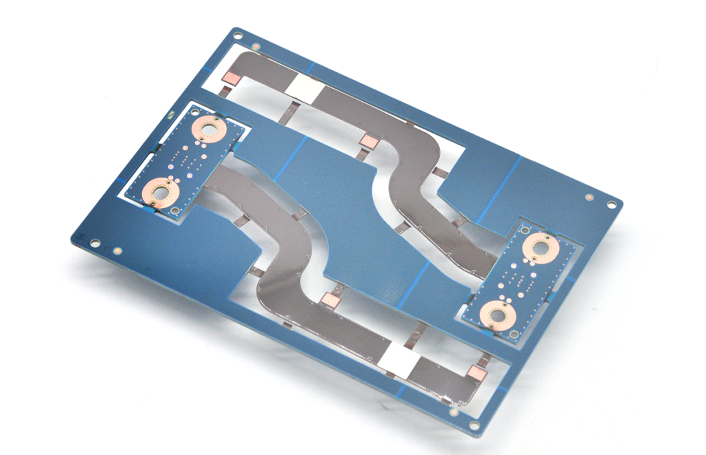
In terms of the number of layers, choose the appropriate number of layers. Single-layer PCBs and double-layer PCBs are suitable for medium and low-density wiring or low-integrity circuits. Based on manufacturing cost considerations, most consumer electronic products rely on single-layer PCBs or double-layer PCBs. However, due to their structural defects, they both generate a lot of EMI, and they are also sensitive to external interference. Multi-layer PCBs tend to be more used in high-density wiring and high-integrity chip circuits. Therefore, when the signal frequency is high and the electronic components are densely distributed, a PCB with at least 4 layers should be selected. In multi-layer PCB design, the power layer and the ground layer should be specially arranged, and the distance between the signal line and the ground line should be reduced.
6. EMI shielding
Shielding and filtering can minimize the impact of EMI. Some shielding and filtering options include:
- Component and PCB shielding
- Low-pass filtering
- Cable shielding
7. Trace routing
Put the current signals with the same output but opposite directions in parallel to eliminate magnetic interference. Discontinuities in printed leads should be minimized. For example, the lead width should not change abruptly and the lead angle should not exceed 90°.
8. Routing design
The power line, ground line, and traces on the circuit board should maintain low impedance to high-frequency signals. When the frequency remains so high, the power line, ground line, and circuit board traces all become small antennas responsible for receiving and transmitting interference. To overcome this interference, it is more important to reduce the high-frequency impedance of the power line, ground line, and circuit board traces than to increase the filter capacitor. Therefore, the traces on the circuit board should be short, thick, and evenly arranged.
9. Decoupling and grounding
The proper placement of decoupling capacitors and the application of the inductor capacitor energy storage function make it possible to provide current to the device at the moment of switching. In a DC loop, load changes can cause power supply noise. The decoupling capacitor configuration can block the noise generated by load changes. For electronic equipment, grounding is a key method to control interference. If grounding is properly combined with shielding measures, most interference problems will be solved.
Above all are the key points when design pcb, hope you can take them in mind and use in your actual design phase.


