What is Flip-Chip Packaging?
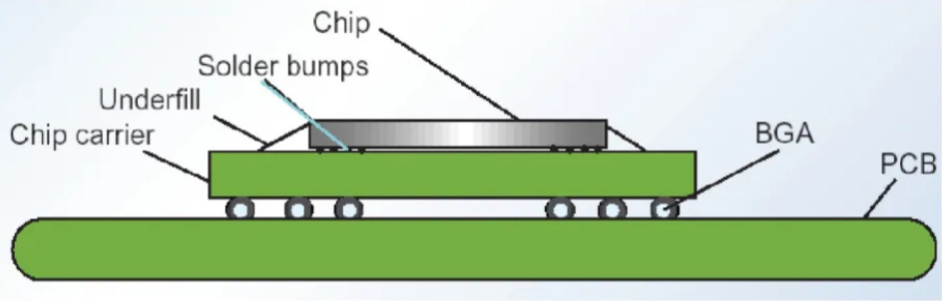
Flip chip is a leadless structure that generally contains circuit units. The term “flip chip” comes from the process of flipping the die upside down during mounting. Solder balls made of tin-lead are deposited on the I/O pads, and then the chip is flipped and heated so that the molten tin-lead balls bond with the ceramic substrate. This technique replaces conventional wire bonding and is gradually becoming the mainstream in packaging technology, currently primarily used in high-clock-rate products such as CPUs, GPUs (Graphic Processor Units), and chipsets. Compared to COB (Chip on Board), the structure of flip-chip packages has the chip and I/O ends (solder balls) facing downward. Since the I/O terminals are distributed across the entire surface of the chip, flip-chip packaging has reached its peak in terms of packaging density and processing speed. In particular, it can be processed using methods similar to SMT (Surface Mount Technology), making it the ultimate direction for chip packaging and high-density assembly.
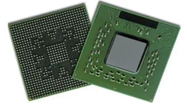
Flip-chip technology originated in the 1950s with thermocouple welding techniques, but it was not widely applied until the 1990s. In traditional packaging methods, the chip is packaged at the bottom and connected to the package substrate via gold wires. In contrast, flip-chip technology connects the active side of the integrated circuit chip (the side with the circuit pattern) face-down directly to the substrate through solder bumps, thereby achieving circuit connections.
What is the Main Advantage of a Flip-Chip Packages?
Compared to traditional wire bonding processes, flip-chip packaging technology offers many distinct advantages, including superior electrical and thermal performance, higher I/O pin count, and reduced package size.
The thermal performance of flip-chip packaging is significantly better than that of conventional wire bonding processes. Today, many electronic devices such as ASICs, microprocessors, and SoCs dissipate power between 10-25W, or even more. In contrast, enhanced heat-dissipation BGA devices using wire bonding can only dissipate between 5-10W. Based on operating conditions, thermal requirements (maximum junction temperature), ambient temperature, and airflow, along with packaging parameters (such as external heatsinks, package size, substrate layers, and the number of solder balls), flip-chip packaging typically supports power dissipation of up to 25W.
The exceptional thermal performance of flip-chip packaging is determined by its low thermal resistance and structure. Heat generated by the chip is dissipated through thermal solder balls and internal and external heatsinks. The close contact between the thermal pad and the chip surface results in low junction temperatures (θjc). To reduce thermal resistance between the thermal pad and the chip, a high thermal conductivity adhesive is applied between them, making it easier for heat to dissipate within the package. For further improvement in thermal performance, an external heatsink can be directly mounted on the thermal pad to achieve even lower junction temperatures (θjc).
Another key advantage of flip-chip packaging is its electrical performance. Wire bonding processes have become bottlenecks for high-frequency and certain applications, while flip-chip technology improves electrical performance. Many electronic devices today operate at high frequencies, making signal integrity a crucial factor. In the past, the frequency limit for IC packaging was around 2-3GHz. With flip-chip packaging, depending on the substrate technology used, it can reach frequencies as high as 10-40GHz.
Flip-Chip Package Acceptance Criteria
Flip-chip packages, like any electronic component, must meet specific acceptance criteria to ensure they function as intended and maintain long-term reliability. These criteria primarily focus on the physical integrity of the die and bumps, as well as electrical performance.
- Bump Integrity: The solder bumps must be intact and free from cracks, voids, or excessive deformation. Even small imperfections can lead to electrical failures over time due to mechanical stress or thermal cycling.
- Chipped Die Edges: While some minor chipping at the die edges may be acceptable, chips that extend too close to the active area of the die can compromise the electrical performance and reliability. Typically, acceptance criteria specify the maximum allowable chip size and proximity to critical areas.
- Solder Joint Strength: The strength of the solder joints between the bumps and the substrate must be sufficient to withstand thermal and mechanical stresses during normal operation. Weak or poorly formed joints can result in electrical discontinuities or complete failure of the device.
- Electrical Performance: The electrical connections between the die and substrate must meet specific resistance and capacitance requirements. Any deviation from these parameters could lead to performance issues or signal integrity problems.
- Thermal Performance: Flip-chip packages must be capable of dissipating heat effectively. If the package does not meet thermal performance criteria, it may overheat, leading to reduced performance or even damage to the device.
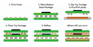
Flip-Chip Packaging Process
1. Inspection and Sorting: The chips are inspected and classified to ensure quality.
2. Adhesion: Conductive glue or solder balls are applied to the IC contact points of the chip.
3. Flip: The chip is flipped onto the PCB substrate using flipping equipment, aligning the chip’s contact points with the substrate.
4. Soldering: The chip contact points are soldered to the metal wiring on the substrate through methods such as thermocompression or thermal cooling.
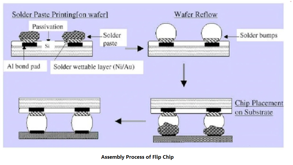
5. Encapsulation: The entire chip is encapsulated using resin or other packaging materials to protect it from external environmental factors.
6. Testing: Functional testing is conducted on the encapsulated chip to ensure it operates correctly.
It is worth mentioning that flip-chip packaging technology faces some challenges during its development. First, since the chip is flipped onto the substrate, the active surface of the chip is exposed, which requires higher protection standards. Second, as the size and spacing of the solder bumps decrease, the alignment precision between the chip and the substrate becomes increasingly critical. Lastly, as packaging density increases, heat dissipation issues become more prominent.
What Are the Different Types of Flip Chips?
Flip chips can be categorized into different types based on their different packages:
1. Flip Chip Ball Grid Array (FCBGA)
Flip Chip Ball Grid Array (FCBGA) is a type of packaging where the die is flipped and connected to a substrate using an array of solder balls. The solder balls are arranged in a grid on the bottom of the package, providing both electrical and mechanical connections. FCBGA is commonly used in high-performance processors like CPUs and GPUs due to its ability to handle high pin counts, excellent electrical performance, and efficient heat dissipation.
2. Flip Chip Chip Scale Package (FCCSP)
Flip Chip Chip Scale Package (FCCSP) refers to a packaging method where the package size is only slightly larger than the die itself. In this type, the die is flipped and mounted directly onto a substrate or carrier using solder bumps. FCCSP is typically used in small form factor devices like mobile phones, tablets, and other compact electronics where space-saving is crucial. It offers better electrical performance and higher packaging density compared to traditional wire-bonded CSP.
3. Flip Chip System in Package (SiP)
SiP integrates multiple components, such as chips, passive components, and sensors, into a single package. The flip chip method allows for denser interconnections within the package, improving overall performance and reducing the footprint. SiP technology is used in applications like mobile devices, wearable technology, and IoT devices where multi-functionality in a compact form is essential.
How Does a Flip Chip Work?
A flip chip works by directly connecting the active side of the semiconductor die to the substrate through solder bumps. These bumps form the electrical pathways between the die and the external circuitry. Once the bumps are reflowed, they solidify into robust electrical connections. The underfill material provides additional mechanical support and helps manage thermal expansion differences between the die and substrate.
The absence of long wire bonds significantly reduces signal latency and noise, making flip-chip packages ideal for high-frequency and high-speed applications. The direct contact also allows for better heat dissipation.
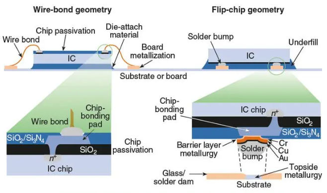
What is the Difference Between Wire Bond and Flip Chip Packaging?
Wire bond packaging and flip-chip packaging are two distinct methods of connecting a semiconductor die to a substrate. They differ in different connection methods, electrical path lengths, applicable scenarios, and multi-chip stacking capabilities.
Connection Method
In wire bonding packaging, the chip is placed face up, and its connections to the circuit board are made through wires (usually gold wires). In contrast, flip-chip packaging uses bumps on the chip to directly interconnect components by flipping them face down onto the substrate, carrier, or circuit board. The electrical side is facing down, essentially flipping the traditional wire bonding method, which is why it’s called “flip chip.”
Electrical Path Length
Wire bonding has a longer electrical path, making it unsuitable for newer devices that require high-speed operation. In comparison, the electrical path in flip-chip packaging is only a fraction of that in wire bonding, making it highly suitable for high-speed operations.
Applicable
Wire bonding is widely used in mobile devices that don’t require fast operations, such as mobile DRAM and NAND chips, due to its cost-effectiveness and reliability. On the other hand, flip-chip packaging, with its shorter electrical path and higher I/O capabilities, is used for packaging high-speed components like CPUs, GPUs, and high-speed DRAM chips.
Multi-Chip Stacking Capability
Wire bonding faces challenges with multi-chip stacking due to the presence of wires, making it less ideal for high-density storage products. Flip-chip packaging, however, allows for denser interconnections in a smaller space, supporting multi-chip stacking and enabling faster data processing.
What is the Difference Between Flip Chip and WLCSP?
Flip-chip packaging and Wafer-Level Chip-Scale Packaging (WLCSP) are both methods of connecting semiconductor dies to external circuitry, but they have important differences:
In flip-chip packaging, the die is mounted onto a separate substrate or PCB. The bumps or solder balls are on the active side of the die, and the assembly is completed after the die is cut from the wafer.
However, in WLCSP, the packaging process occurs directly at the wafer level before the individual dies are cut. The solder bumps are applied while the die is still part of the wafer, and the final package is essentially the same size as the die itself. WLCSP is ideal for applications where size is critical, such as mobile devices, while flip-chip packaging is used for high-performance applications requiring greater thermal and electrical capabilities.
What is a Flip Chip Used For?
Flip-chip packaging is used in a wide variety of applications, particularly those that require high performance, small size, and efficient thermal management. Some common uses include:
- Mobile devices
- Networking equipment
- Automotive electronics
- Cell phones
- Handheld electronics
- GPS
- PC peripherals
- Voltage regulators
- High-speed memory
- Camcorders
- DVD
- Digital cameras
- Game console
- Graphics and chipsets for pcs
- Servers
- Microprocessor for pc and servers
- Memory
This is the end of this sharing, welcome to contact us if you have any questions.