pcb
Home > Blog

Posts Tagged ‘high frequency pcb’

Rogers RT Duroid 5880 | High Frequency Rogers RO5880 PCB Manufacturer
Wednesday, October 16th, 2024

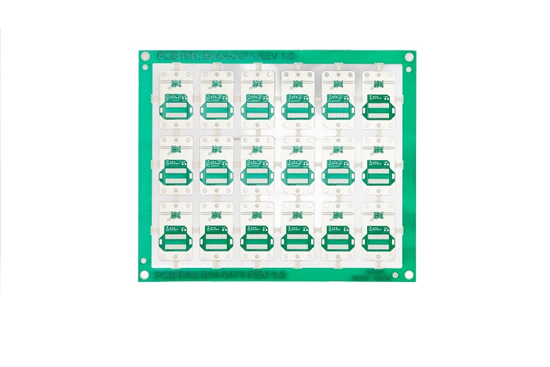
What substrate is Rogers RT Duroid 5880?

Rogers RT Duroid 5880 is a high-frequency laminate specifically designed for applications where precision and low signal loss are critical. The substrate is a composite material known for its excellent performance in RF and microwave circuits. It uses a PTFE (polytetrafluoroethylene) base reinforced with glass microfibers.

The use of glass microfiber ensures the material is durable but lightweight, making it suitable for applications in which weight is a factor. Its composition is perfect for projects where high-frequency signals are involved. From defense systems to automotive radar, RT Duroid 5880 is a reliable choice. It has become the go-to substrate for engineers and designers looking for efficiency, precision, and durability.

Rogers RT Duroid 5880 | High Frequency Rogers RO5880 PCB Manufacturer

Composition of Rogers RT/duroid 5880

RT Duroid 5880 is composed of PTFE (polytetrafluoroethylene) combined with glass microfiber. PTFE provides a low dissipation factor, which reduces signal loss. This is important for maintaining high performance in RF and microwave applications. Glass microfiber reinforces the material, make it stronger without adding unnecessary weight. The composition also includes copper cladding, which is typically laminated on both sides. The copper layer helps with conductivity, ensuring signals travel efficiently across the board.

The unique combination of PTFE and glass microfiber gives RT Duroid 5880 its excellent mechanical stability. It also minimizes the effect of temperature changes, which is critical for high-frequency circuits. As a result, the material can handle extreme temperatures without affecting the performance of the PCB.

RT/duroid 5880 Specifications

The following table highlights the important specifications of Rogers RT Duroid 5880. These specs reflect the high performance of RT Duroid 5880 for complex RF and microwave tasks.

PropertyValue
Dielectric Constant (Dk)2.20 (±0.02)
Dissipation Factor (Df)0.0004 (measured at 10 GHz)
Thermal Conductivity0.20 W/m/K
Operating Temperature Range-55°C to +150°C
Water Absorption0.02%
Volume Resistivity1.7 x 10^9 MΩ·cm (minimum)
Surface Resistivity1.4 x 10^8 MΩ (minimum)
Coefficient of Thermal Expansion (CTE)46 ppm/°C (in X-Y axis)
Tensile Strength10.3 MPa
FlammabilityUL 94 V-0
Peel Strength5.0 N/mm (after soldering)

RT/duroid 5880 Thickness

RT Duroid 5880 comes in various thicknesses. Engineers can choose the right thickness depending on their project’s needs. Rogers RT/duroid 5880 laminate is commercially available in sheet stock and roll stock forms in a range of thicknesses. Here’s a list of the standard thicknesses available:

Available sheet sizes:

  • 304.8 x 457.2 mm
  • 457.2 x 609.6 mm
  • 609.6 x 914.4 mm

Standard thickness:

  • 0.127 mm (5 mils)
  • 0.254 mm (10 mils)
  • 0.381 mm (15 mils)
  • 0.508 mm (20 mils)
  • 0.787 mm (31 mils)
  • 1.524 mm (60 mils)
  • 3.175 mm (125 mils)

Available roll widths:

  • 304.8 mm
  • 609.6 mm
  • 1219.2 mm
  • Standard roll length: 76.2 meters
  • Thickness range: 0.127 mm to 1.575 mm ​

RO5880 RF PCB Advantages

Rogers RT Duroid 5880 has a lot of strengths when used in RF and microwave PCB projects:

  • Minimal Signal Loss

With a low dissipation factor of 0.0004, it reduces signal loss, which is very helpful for high-frequency systems like radar or satellite communications.

  • Strong Stability

It holds up well under temperature changes and in humid environments, keeping circuits running smoothly even in tough conditions.

  • Reliable Electrical Properties

The dielectric constant of 2.20 remains stable over a range of frequencies. This helps keep circuits working consistently without interference or signal issues.

  • Heat Tolerance

It withstands heat up to 150°C, making it a good choice for systems that need to handle higher temperatures.

  • Low Moisture Absorption

With only 0.02% water absorption, the material works well in damp environments. Outdoor systems like antennas benefit from this.

  • Ease of Manufacturing

The material is easy to work with during production, which keeps costs lower and speeds up manufacturing.

  • Chemical Resistance

The PTFE base resists damage from chemicals and solvents, making the material last longer in harsh environments like aerospace and industrial applications.

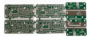
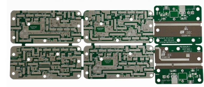
Typical Applications of High-Frequency PCB

High-frequency PCBs built with Rogers RT Duroid 5880 serve important roles across many industries:

  • Aerospace – used in radar, satellite, and navigation systems, RT Duroid 5880 supports reliable communication and tracking, even in high-pressure environments.
  • Telecommunications – in mobile networks, base stations, and antennas, high-frequency PCBs help maintain clear and fast data transmission, supporting the backbone of communication systems.
  • Medical Devices – MRI machines, wireless health monitors, and other equipment use high-frequency PCBs to keep medical data accurate and systems working seamlessly.
  • Defense – communication gear, and electronic warfare systems.
  • Automotive Systems – advanced driver assistance systems (ADAS) and vehicle radar depend on high-frequency PCBs for real-time data, making roads safer for everyone.
  • Satellite Communication – RT Duroid 5880 is frequently used in satellite systems where strong signal transmission over long distances is crucial for communication networks.

Common-Used High Frequency PCB Materials in Best Technology

At Best Technology, we use a range of top-quality materials for high-frequency PCBs, depending on the project’s needs. Some of the most popular materials include:

Material       Dielectric Constant (Dk)      Loss Tangent (Df)       Key Features  
Rogers RO4003C3.380.0027Low loss, excellent thermal stability, ideal for RF applications.
Rogers RO43503.480.0043Low loss, high thermal conductivity, suitable for microwave applications.  
RT/Duroid RO58802.940.0037Very low loss, excellent performance at high frequencies, good for multilayer designs.  
N4000-133.00.009Good thermal stability, low moisture absorption, designed for high-frequency applications.
Taconic RF-60A6.150.0027High dielectric constant, low loss, suitable for low-loss RF and microwave applications.  

Each material brings different strengths for specific applications, giving you the best options for your project.

Discuss Your High Frequency PCB Project with Us Today

If you have a high-frequency PCB project in mind, reach out to us. We’re experienced in creating high-quality PCBs that meet your exact specifications. Whether you need RF, microwave, or other types of high-frequency boards, we’ll make sure your project runs smoothly. Contact us at sales@bestpcbs.com today, and we’ll help you turn your plans into reality.

You may also like

High Frequency PCB & High Frequency PCB Prototype
Friday, September 20th, 2024

What is High-Frequency PCBs?

What is High-Frequency PCBs? High frequency PCBs are specifically designed to operate at frequencies typically above 1GHz. These circuit boards play a crucial role in modern communication systems like satellite communications, radar, and wireless networks. The materials used in high-frequency PCBs are different from those in standard PCBs. While standard PCBs use FR4 material, high-frequency PCBs often require specialized materials like PTFE (Teflon) or Rogers material to reduce signal loss and improve overall performance.

The growing need for faster and more reliable communication across industries makes high-frequency PCBs essential for creating cutting-edge devices.

High Frequency PCB Materials

Click here to download Raw Materials of RF PCB.

Advantages of High Frequency PCB

  • Faster signal transmission
  • Better signal integrity
  • Enhanced thermal management
  • Low electromagnetic interference (EMI)
  • Application in emerging technologies
  • Improved precision in high-speed applications

What is the Frequency Limit for FR4 PCB?

FR4 is the most widely used material in standard PCBs due to its affordability and adequate performance for general applications. However, when it comes to high-frequency operations, FR4 has its limitations. The material can handle frequencies up to about 1GHz, but beyond this range, its performance starts to degrade significantly. High-frequency signals experience increased signal loss, dielectric losses, and electromagnetic interference (EMI) due to FR4’s higher dielectric constant (around 4.5) and poor thermal properties.

The limitations make FR4 unsuitable for more advanced applications like high-speed telecommunications, radar systems, and modern wireless technologies where signals operate in the gigahertz range. When designing PCBs that require frequencies beyond 1GHz, alternative materials like PTFE (Teflon) or Rogers laminates are recommended to maintain signal integrity and reduce losses.

How Do You Make High-Frequency PCB?

Creating a high-frequency PCB involves a few additional considerations compared to standard PCB designs. First, the choice of materials is critical. PTFE, Rogers, and other high-performance laminates are commonly used to ensure the PCB can handle high-frequency signals. Next, the board’s thickness, trace width, and layout need to be carefully calculated to avoid impedance issues. The key process including:

1. Material Selection

The first step is choosing materials that can handle high-frequency signals. Materials like PTFE, Rogers, or ceramic substrates are commonly used because they have lower dielectric constants, low dissipation factors, and better thermal stability. These materials ensure minimal signal degradation.

2. Controlled Impedance

High-frequency signals are sensitive to variations in impedance. Controlled impedance design ensures that the trace impedance matches the signal’s requirements, preventing reflection and signal distortion. This involves calculating the width and spacing of the traces and ensuring consistent dielectric properties across layers.

3. Multi-layer PCB

Multi-layer boards are often necessary for high-frequency applications to separate signals and reduce cross-talk. Ground planes are typically added to lower electromagnetic interference (EMI) and provide better signal grounding.

4. Short and Direct Signal Paths

Keeping signal paths as short as possible helps minimize signal loss and prevents unwanted interference. Traces that are too long or involve sharp bends can introduce delay and noise.

5. Shielding

In some cases, shielding techniques can be employed to prevent interference from other electronic components. This can include grounded planes, copper shields, or even encapsulating certain areas of the PCB.

High-frequency PCB design often requires sophisticated simulation tools. Software such as Ansys or Altium Designer helps predict how signals will behave on the board, allowing for adjustments to be made before fabrication.

What is the Highest RF Frequency?

In communication circuits, radio frequency (RF) bands cover a wide range of frequencies, typically starting from 20kHz up to 300GHz. The highest RF frequency currently used in commercial applications ranges from 100GHz to 300GHz, categorized as millimeter waves. These frequencies are essential for high-speed data transmission in technologies like 5G, radar systems, and advanced satellite communication. While developing PCBs that can efficiently handle such frequencies can be challenging, material innovations have made it possible.

What Are Some Important Considerations When Designing a PCB Layout for High-Frequency Circuits?

Designing a PCB for high-frequency circuits demands a careful approach to ensure signal integrity. The first thing to consider is the dielectric material. As previously mentioned, materials like Rogers or PTFE are preferred because they offer lower dielectric loss, which is crucial at higher frequencies. Trace layout is another critical factor. The length and width of the traces must be calculated to maintain impedance control, ensuring that signals don’t get distorted as they travel through the board.

1. Signal Integrity and Trace Layout

The layout of traces is a critical consideration in high-frequency PCB design. To maintain signal integrity, traces should be kept as short and straight as possible. Long traces can introduce delay, noise, and signal degradation. Additionally, sharp corners in trace routing should be avoided because they can lead to signal reflection and impedance discontinuities. Rounded or 45-degree bends are preferable to right-angle corners, which can cause unwanted signal interference.

2. Ground Planes and Layer Stack-Up

A solid, continuous ground plane is one of the most effective ways to reduce noise and EMI in high-frequency PCBs. Ground planes provide a low-impedance path for return currents and act as shields to prevent electromagnetic radiation from affecting other components. For multi-layer PCBs, having dedicated power and ground planes in the stack-up helps reduce noise and improves overall signal integrity.

3. Via Management

Vias introduce small inductances into the signal path, which can become problematic in high-frequency circuits. High-frequency signals are particularly sensitive to these inductances, and excessive use of vias can degrade signal quality. Designers should minimize the number of vias in high-frequency signal paths and use smaller, controlled-depth vias like microvias or buried vias to reduce parasitic effects.

4. Signal Isolation

High-frequency circuits often involve both analog and digital signals, and proper isolation between these signals is critical to prevent interference. Digital signals tend to generate high levels of noise, which can interfere with sensitive analog signals. To avoid this, analog and digital components should be physically separated on the PCB, with separate ground planes if possible.

5. Power Distribution and Decoupling

Stable power distribution is necessary to ensure that high-frequency components operate without interruptions. A decoupling capacitor should be placed near the power supply pins of each active component to filter out high-frequency noise and maintain a steady voltage. Multiple capacitors of different values (e.g., 0.1µF and 10µF) can be used in parallel to filter noise over a wide frequency range.

How Do You Avoid High-Frequency Interference in PCB?

Interference is a common issue in high-frequency PCBs, but it can be managed with the right design techniques. The most effective way to avoid high-frequency interference is by using a dedicated ground plane. This plane acts as a shield, helping to reduce EMI and cross-talk between different parts of the circuit. Shielding can also be applied to individual traces or components that are more susceptible to interference.

  • Ground Planes

A continuous ground plane is one of the most effective ways to reduce high-frequency interference. It acts as a shield and prevents unwanted noise from penetrating the circuit. The use of multiple ground planes in multi-layer PCBs can also provide better signal grounding.

  • Signal Layer Segregation

Isolating analog and digital signals helps to reduce interference between them. Analog signals are more susceptible to noise, so they should be kept separate from high-frequency digital signals.

  • Shorter Traces

Keeping traces short and direct minimizes the potential for signal loss or delay, and helps maintain signal integrity. The longer the trace, the more likely it is to pick up unwanted noise.

  • Minimize Via Usage

Excessive use of vias can create points of discontinuity in the signal path, leading to reflections and noise. If vias are necessary, they should be placed strategically and sparingly.

  • EMI Shielding

In some cases, it may be necessary to use EMI shields around particularly sensitive areas of the PCB.

  • Decoupling Capacitors

Adding decoupling capacitors between the power supply and ground helps to filter out high-frequency noise and maintain a clean signal.

What is the Difference Between High-Speed and High-Frequency PCB?

Though they may seem similar, high-speed and high-frequency PCBs serve different purposes. High-speed PCBs are designed to handle fast data transmission speeds, often used in applications like computing and networking. These PCBs focus on minimizing delay and ensuring signals reach their destination without distortion.

On the other hand, high-frequency PCBs are specifically optimized for circuits operating at high frequencies, often in communication systems. The emphasis here is on maintaining signal integrity across a wide frequency range. While both high-speed and high-frequency PCBs share common design principles, such as controlled impedance and signal integrity, the challenges they face differ. High-speed PCBs focus more on data transmission, while high-frequency PCBs deal with RF signals and the challenges of maintaining signal strength at higher frequencies.

How Do You Fix Frequency Interference?

If your PCB is experiencing frequency interference, there are several methods to fix the problem. One common approach is to improve grounding by using a continuous ground plane. This helps shield signals from external noise and interference. You can also add shielding to specific components or traces that are particularly susceptible to interference.

Adding filters at key points in your circuit can help block unwanted frequencies. For instance, a low-pass filter allows only low-frequency signals to pass through, blocking higher-frequency interference. You can also reduce trace lengths and maintain clean, direct paths for high-frequency signals. Finally, proper isolation of analog and digital circuits is crucial to prevent noise from leaking into sensitive areas.

You may also like