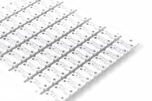
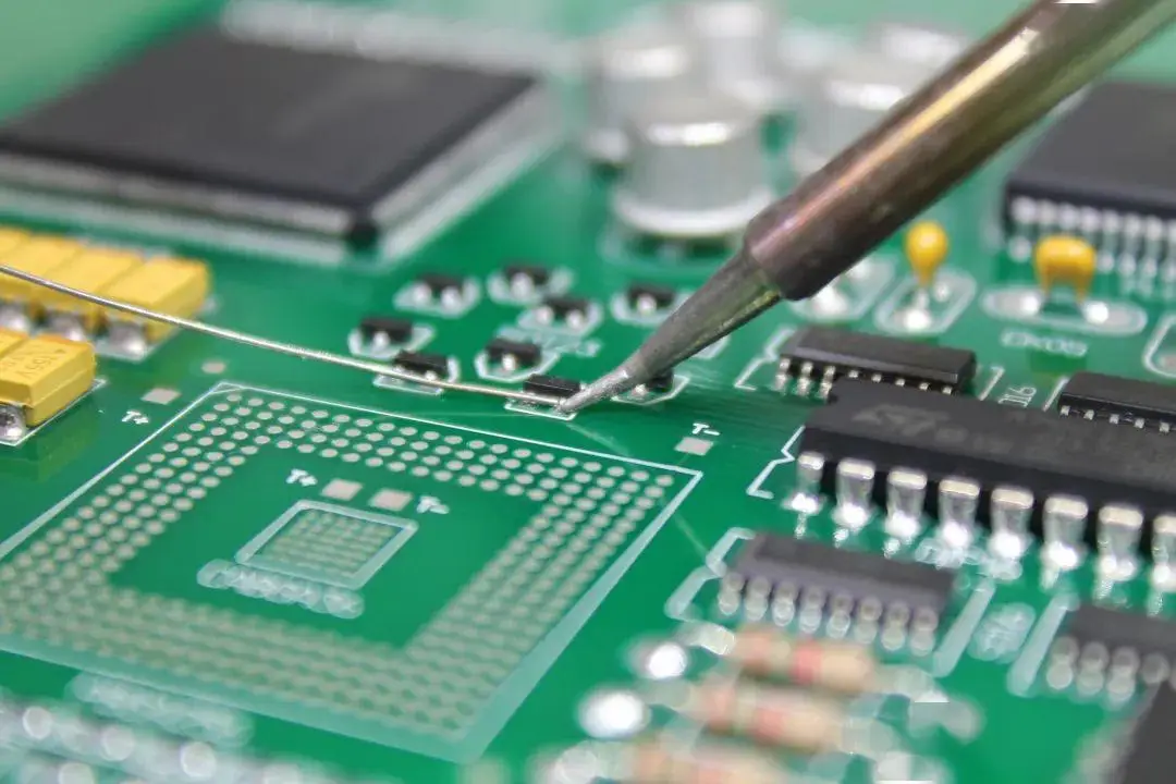
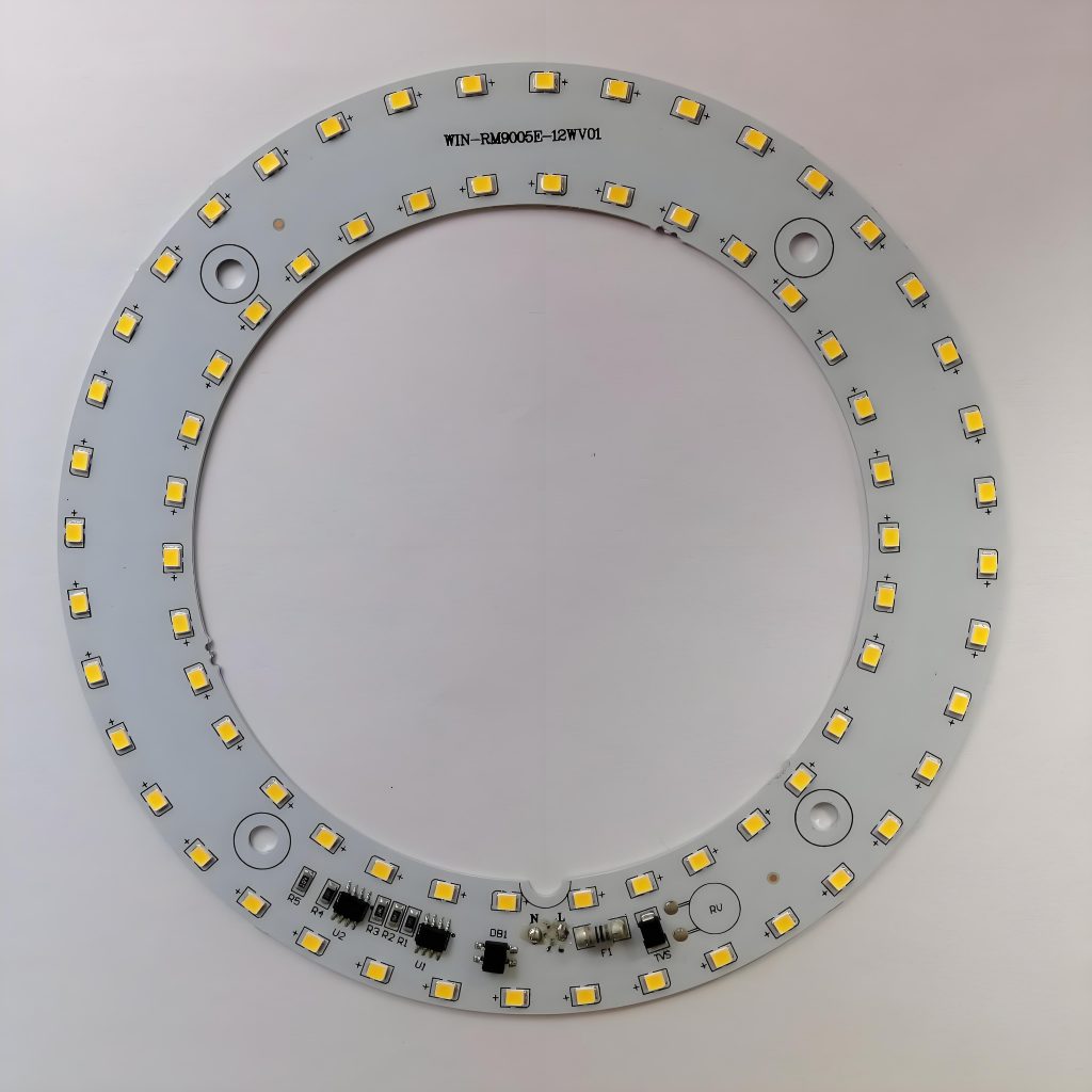
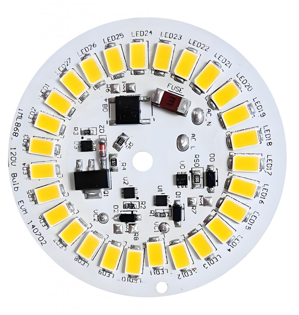
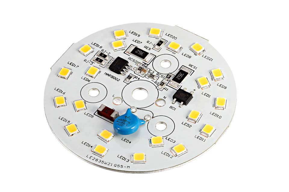
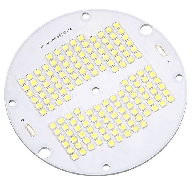
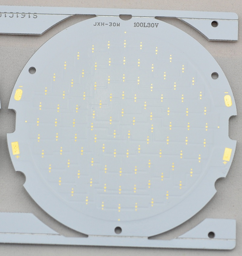
LED switching power supply PCB board design,In the design of switching power supplies, if the PCB board is not designed properly, it will radiate too much electromagnetic interference. The following seven tricks are summarized for the design of PCB boards that ensure stable power supply operation: by analyzing the matters that need to be paid attention to in each step, you can easily design the PCB board step by step!
Step 1
Design process from schematic to PCB: Establish component parameters – > Input schematic netlist – > Design parameter setting – > Manual layout – > Manual wiring – > Verify design – > Review – > CAM output.
Step 2
Parameter setting: The spacing between adjacent wires must meet the electrical safety requirements, and the spacing should be as wide as possible for easy operation and production. The spacing should at least be suitable for the voltage to be tolerated. When the wiring density is low, the spacing between signal lines can be appropriately increased. The signal lines with high and low levels should be as short as possible and the spacing should be increased. In general, the wiring spacing is set to 8mil. The distance from the edge of the inner hole of the pad to the edge of the printed circuit board should be greater than 1mm to avoid pad defects during processing. When the trace connected to the pad is thin, the connection between the pad and the trace should be designed into a water drop shape. The advantage of this is that the pad is not easy to peel, but the trace and the pad are not easy to disconnect.
Step 3
Component layout practice has proved that even if the circuit schematic is designed correctly, improper printed circuit board design will have an adverse effect on the reliability of electronic equipment. For example, if two thin parallel lines on a printed circuit board are very close to each other, a delay in the signal waveform will be formed, and reflected noise will be formed at the end of the transmission line; interference caused by inconsiderate consideration of the power supply and ground line will reduce the performance of the product. Therefore, when designing a printed circuit board, you should pay attention to using the correct method. Each switching power supply has four current loops:
(1) Power switch AC loop
(2) Output rectifier AC loop
(3) Input signal source current loop
(4) Output load current loop
The input loop charges the input capacitor through a current that is close to DC, and the filter capacitor mainly plays a broadband energy storage role; similarly, the output filter capacitor is also used to store high-frequency energy from the output rectifier and eliminate the DC energy of the output load loop. Therefore, the terminals of the input and output filter capacitors are very important. The input and output current loops should be connected to the power supply only from the terminals of the filter capacitors; if the connection between the input/output loop and the power switch/rectifier loop cannot be directly connected to the terminals of the capacitor, the AC energy will be radiated from the input or output filter capacitor to the environment. The AC circuit of the power switch and the AC circuit of the rectifier contain high-amplitude trapezoidal currents. The harmonic components in these currents are very high, and their frequencies are much higher than the switching base frequency. The peak amplitude can be as high as 5 times the continuous input/output DC current amplitude, and the transition time is usually about 50ns. These two circuits are prone to electromagnetic interference, so these AC circuits must be laid out before other printed wiring in the power supply. The three main components of each circuit, filter capacitors, power switches or rectifiers, and inductors or transformers, should be placed adjacent to each other, and the positions of the components should be adjusted to make the current path between them as short as possible.
The method of establishing the layout of the switching power supply is similar to its electrical design. The design process is as follows:
Place the transformer Design the power switch current loop Design the output rectifier current loop Control circuit connected to the AC power circuit Design the input current source loop and input filter Design the output load loop and output filter According to the functional units of the circuit, when laying out all the components of the circuit, the following principles must be met:
(1) First, consider the size of the PCB. When the PCB size is too large, the printed lines are long, the impedance increases, the anti-noise ability decreases, and the cost increases; if it is too small, the heat dissipation is poor, and the adjacent lines are susceptible to interference. The shape of the circuit board is rectangular, with an aspect ratio of 3:2 or 4:3. The components located at the edge of the circuit board are generally not less than 2mm away from the edge of the circuit board.
(2) When placing components, consider the subsequent welding and do not place them too densely;
(3) The components of each functional circuit are centered and the layout is carried out around it. The components should be arranged evenly, neatly and compactly on the PCB. The leads and connections between the components should be minimized and shortened as much as possible, and the decoupling capacitor should be as close to the VCC of the device as possible.
(4) For circuits working at high frequencies, the distribution parameters between components should be considered. Generally, the components of the circuit should be arranged in parallel as much as possible. This is not only beautiful, but also easy to assemble and solder, and easy to mass produce.
(5) Arrange the positions of each functional circuit unit according to the circuit process, so that the layout is convenient for signal flow and the signal keeps the same direction as much as possible.
(6) The first principle of layout is to ensure the wiring pass rate. When moving components, pay attention to the connection of flying wires and put the components with connection relationships together.
(7) Reduce the loop area as much as possible to suppress the radiation interference of the switching power supply.
Step 4
Wiring The switching power supply contains high-frequency signals. Any trace on the PCB can act as an antenna. The length and width of the trace will affect its impedance and inductance, thereby affecting the frequency response. Even traces that pass DC signals can couple to RF signals from adjacent traces and cause circuit problems (even radiate interference signals again). Therefore, all traces that pass AC current should be designed to be as short and wide as possible, which means that all components connected to the traces and to other power lines must be placed very close. The length of the trace is proportional to the inductance and impedance it exhibits, while the width is inversely proportional to the inductance and impedance of the trace. The length reflects the wavelength of the trace response. The longer the length, the lower the frequency of the electromagnetic wave that the trace can send and receive, and it can radiate more RF energy. According to the size of the printed circuit board current, try to increase the width of the power line and reduce the loop resistance. At the same time, make the direction of the power line and ground line consistent with the direction of the current, which helps to enhance the anti-noise ability. Grounding is the bottom branch of the four current loops of the switching power supply. It plays an important role as a common reference point of the circuit. It is an important method to control interference. Therefore, the placement of the grounding wire should be carefully considered in the layout. Mixing various groundings will cause unstable power supply operation.
The following points should be noted in the grounding design:
- Correctly select single-point grounding. Usually, the common end of the filter capacitor should be the connection point where other grounding points are coupled to the AC ground of large current. The grounding points of the same circuit should be as close as possible, and the power filter capacitor of the circuit at this level should also be connected to the grounding point of this level. The main consideration is that the current flowing back to the ground from each part of the circuit is changing. The impedance of the actual flowing line will cause the ground potential of each part of the circuit to change and introduce interference. In this switching power supply, the inductance between its wiring and devices has little effect, while the loop current formed by the grounding circuit has a greater impact on interference. Therefore, a single-point grounding is used, that is, the ground wires of several devices in the power switch current loop are connected to the ground pin, and the ground wires of several devices in the output rectifier current loop are also connected to the ground pin of the corresponding filter capacitor. In this way, the power supply works more stably and is not easy to self-excite. When a single point cannot be achieved, two diodes or a small resistor are connected to the common ground. In fact, it can be connected to a relatively concentrated piece of copper foil.
- Try to thicken the ground wire. If the ground wire is very thin, the ground potential changes with the change of current, causing the timing signal level of the electronic equipment to be unstable and the anti-noise performance to deteriorate. Therefore, it is necessary to ensure that each large current ground end uses a printed line as short and wide as possible, and try to widen the width of the power and ground wires. The ground wire is wider than the power line. Their relationship is: ground wire>power line>signal line. If possible, the width of the ground wire should be greater than 3mm, or a large copper layer can be used as a ground wire. On the printed circuit board, all unused areas are connected to the ground as ground wires. When performing global wiring, the following principles must be followed:
(1) Wiring direction: From the welding surface, the arrangement of components should be kept consistent with the schematic diagram as much as possible, and the wiring direction should be consistent with the wiring direction of the circuit diagram. Because various parameters usually need to be tested on the welding surface during the production process, this is convenient for inspection, debugging and maintenance during production (Note: It refers to the premise of meeting the circuit performance and the requirements of the whole machine installation and panel layout).
(2) When designing the wiring diagram, the wiring should have as few turns as possible, the line width on the printed arc should not change suddenly, the wire corner should be ≥90 degrees, and the lines should be simple and clear.
(3) No cross circuits are allowed in the printed circuit. For lines that may cross, “drilling” and “winding” can be used to solve them. That is, let a lead “drill” from the gap under the feet of other resistors, capacitors, and transistors In the past, or from one end of a lead that may cross, in special cases, if the circuit is very complicated, in order to simplify the design, it is also allowed to use wire jumper to solve the problem of cross circuit. Because a single-sided board is used, the through-hole components are located on the top surface and the surface-mount components are located on the bottom surface, so when laying out, the through-hole components can overlap with the surface-mount components, but the pads must be avoided from overlapping. - Input ground and output ground This switching power supply is a low-voltage DC-DC. To feed the output voltage back to the primary of the transformer, the circuits on both sides should have a common reference ground, so after the ground wires on both sides are coppered separately, they must be connected together to form a common ground.
Step 5
Inspection: After the wiring design is completed, it is necessary to carefully check whether the wiring design conforms to the rules set by the designer. At the same time, it is also necessary to confirm whether the rules set meet the requirements of the printed circuit board production process. Generally, check whether the distance between lines, lines and component pads, lines and through holes, component pads and through holes, and through holes are reasonable and meet production requirements. Whether the width of the power line and the ground line is appropriate, and whether there is any place in the PCB that can widen the ground line. Note: Some errors can be ignored. For example, part of the outline of some connectors is placed outside the board frame, which will cause errors when checking the spacing; in addition, after each modification of the routing and vias, copper must be re-coated.
Step 6
Review According to the “PCB Checklist”, the content includes design rules, layer definition, line width, spacing, pads, and via settings. It is also necessary to focus on reviewing the rationality of the device layout, the routing of the power and ground network, the routing and shielding of the high-speed clock network, and the placement and connection of the decoupling capacitors.
Step 7
a. The layers that need to be output are the wiring layer (bottom layer), the silk screen layer (including the top silk screen and the bottom silk screen), the solder mask layer (bottom solder mask), the drilling layer (bottom layer), and the drilling file (NCDrill)
b. When setting the layer of the silk screen layer, do not select PartType, select the Outline, Text, and Line of the top (bottom) and silk screen layers
c. When setting the layer of each layer, select Board Outline, and when setting the layer of the silk screen layer, do not select PartType, select the Outline, Text, and Line of the top (bottom) and silk screen layers.
d. When generating the drilling file, use the default settings of PowerPCB and do not make any changes.