Why medical LED PCB? This guide explores design strategies, manufacturer selection, cost optimization, and cutting-edge innovations driving LED-based medical diagnostics, therapy systems, and smart surgical tools.
Best Technology delivers precision medical LED PCB tailored for healthcare innovation. As a certified manufacturer with in-house ISO 13485/9001-compliant production, we ensure medical-grade reliability for surgical, diagnostic, and therapeutic devices. Fast-tracked lead times (15 days or less) and rigorous testing (AOI, thermal cycling) streamline compliance with sterilization and safety standards. Custom solutions include IoT integration, aluminum-core thermal designs, and RoHS-certified materials. Contact us today: sales@bestpcbs.com
What Is Medical LED PCB?
A medical LED PCB (Printed Circuit Board) is a specialized electronic component designed to support and control LED (Light-Emitting Diode) systems in medical devices. These circuit boards are engineered to meet the stringent requirements of healthcare applications, ensuring reliability, precision, and safety in critical medical environments.
What Are Features of LED Medical PCB?
Below are features their defining features:
- High Precision and Stability: Medical LED PCBs ensure consistent performance in critical applications, such as surgical lighting and diagnostic tools. They minimize signal interference and voltage fluctuations, maintaining accuracy in sensitive procedures.
- Compliance with Medical Standards: These PCBs adhere to strict international regulations, including ISO 13485 and IEC 60601, which govern safety and quality in medical electronics. Materials and manufacturing processes align with biocompatibility and sterilization requirements.
- Advanced Thermal Management: Efficient heat dissipation is achieved through specialized copper substrates or ceramic materials. This prevents overheating in prolonged operations, extending LED lifespan and ensuring device reliability.
- Compact and Customizable Design: Medical LED PCBs are often tailored to fit space-constrained devices, such as handheld scanners or endoscopic systems. Their modular layouts allow integration with sensors, drivers, and connectivity modules.
- Durability in Harsh Conditions: Built to withstand repeated sterilization (e.g., autoclaving or UV exposure) and chemical cleaning, these PCBs use protective coatings like conformal silicone to resist moisture and corrosion.
- Low Power Consumption: Optimized circuitry reduces energy usage without compromising brightness, making them ideal for portable or battery-operated medical devices.
- Enhanced Safety Protocols: Features like short-circuit protection and fail-safe mechanisms prevent malfunctions, ensuring patient and operator safety during treatments.
- Compatibility with Digital Systems: Many Medical LED PCBs support IoT connectivity, enabling integration with smart healthcare platforms for real-time monitoring and data analysis.
What Are Application of Medical LED PCBs?
Applications of Medical LED PCBs:
- Surgical Lighting Systems – Medical LED PCBs power high-intensity surgical lights, providing consistent illumination for operating rooms. Their ability to maintain stable brightness and color accuracy ensures optimal visibility during procedures, reducing eye strain for medical teams.
- Phototherapy Devices – Neonatal jaundice treatment often relies on LED-based phototherapy systems. Medical LED PCBs enable controlled blue-light emission, which safely breaks down bilirubin in infants’ blood without generating excessive heat.
- Diagnostic Imaging Equipment – LED arrays in imaging tools like endoscopes depend on medical LED PCBs. These boards deliver precise light wavelengths to enhance tissue visualization, aiding in early detection of conditions such as skin cancer or gastrointestinal issues.
- UV Sterilization Devices – Ultraviolet (UV) LED systems used for disinfecting medical instruments and surfaces incorporate medical LED PCBs. They ensure efficient UV-C light output to eliminate pathogens while resisting damage from repeated exposure to cleaning agents.
- Wearable Health Monitors – Compact medical LED PCBs are embedded in wearable devices, such as pulse oximeters or glucose monitors. They enable non-invasive tracking of vital signs by emitting and detecting specific light wavelengths through the skin.
- Dental Curing Tools – LED-based dental curing lamps use medical LED PCBs to produce targeted blue light for hardening composite resins during fillings or orthodontic treatments. Their precise light control minimizes overheating risks to oral tissues.
- Therapeutic Light Therapy – Chronic pain management and wound healing devices leverage medical LED PCBs to emit red or near-infrared light. These wavelengths stimulate cellular repair and reduce inflammation in conditions like arthritis or diabetic ulcers.
- Laboratory Analyzers – In vitro diagnostic equipment, such as blood analyzers or PCR machines, integrate medical LED PCBs for optical sensing. They ensure accurate fluorescence detection or sample illumination during lab tests.
- Endoscopic Illumination – Medical LED PCBs provide reliable light sources for minimally invasive endoscopic procedures. Their compact design and heat management capabilities prevent tissue damage while illuminating internal organs during surgery.
- Emergency Medical Devices – Portable defibrillators and ventilators use medical LED PCBs for status indicators and display backlighting. Their durability ensures functionality in high-stress emergency scenarios, even in extreme environments.

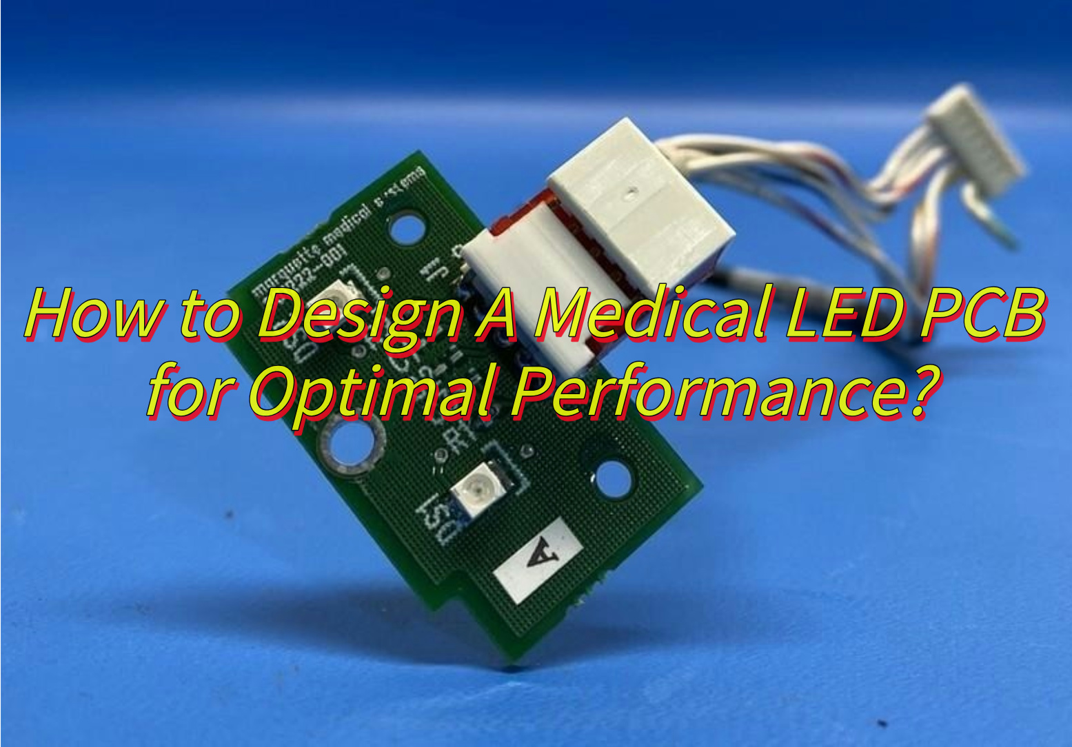
How to Design A Medical LED PCB for Optimal Performance?
This is how to design a medical LED PCB for optimal performance:
- Select High-Performance Materials–Use substrates like aluminum or ceramic for superior heat dissipation. These materials handle high currents and temperatures common in medical devices. For flexible applications, polyimide-based PCBs offer durability in compact designs.
- Prioritize Thermal Management–Integrate thermal vias, heat sinks, or metal-core designs to channel heat away from LEDs. Proper thermal design prevents overheating, ensuring stable light output and prolonging component lifespan.
- Minimize Electromagnetic Interference (EMI)- Implement shielding layers, ground planes, and ferrite beads to suppress EMI. Keep high-frequency traces short and avoid routing them near sensitive analog circuits to comply with medical EMC standards.
- Optimize Circuit Layout for Precision–Use controlled impedance routing for signal integrity. Maintain consistent trace widths and spacing to reduce cross-talk. Place LEDs and drivers close to power sources to minimize voltage drops.
- Ensure Biocompatibility and Sterilization Resistance- Choose conformal coatings like silicone or epoxy that withstand repeated sterilization (e.g., autoclaving, UV-C exposure). Verify materials meet ISO 10993 standards for biological safety.
- Design for Mechanical Robustness: Reinforce solder joints and use thicker copper layers (2 oz+) to withstand vibrations or bending in portable devices. Avoid placing components near board edges to reduce stress during handling.
- Incorporate Redundancy for Critical Components: Duplicate essential circuits, such as current regulators, to maintain functionality if a component fails. This is vital for life-saving equipment like surgical lights or monitors.
- Validate with Rigorous Testing: Perform thermal cycling, HALT (Highly Accelerated Life Testing), and EMI/EMC testing to identify weaknesses. Simulate real-world conditions, including humidity and chemical exposure, to ensure reliability.
- Adhere to Medical Compliance Standards: Follow IEC 60601-1 for electrical safety and ISO 13485 for quality management. Document design choices to streamline FDA or CE certification processes.
- Optimize Power Distribution: Use separate power planes for analog and digital sections to prevent noise coupling. Incorporate voltage regulators with tight tolerances to ensure consistent LED performance.
How to Choose A Wholesale Medical LED PCB Manufacturer?
Here’s how to choose a wholesale medical LED PCB manufacturer:
- Confirm Compliance with Medical Standards - Verify certifications like ISO 13485 (medical device QMS) and IEC 60601-1 (electrical safety). Manufacturers familiar with these frameworks reduce regulatory risks and streamline device approvals.
- Evaluate Material Expertise – Prioritize manufacturers experienced with medical-grade substrates (e.g., aluminum for heat dissipation, FR4 for cost-sensitive applications). They should source UL-listed materials and biocompatible coatings resistant to sterilization.
- Review Advanced Manufacturing Capabilities– Ensure the manufacturer supports high-density interconnect (HDI), laser drilling, and impedance-controlled routing. These features are critical for compact, high-performance LED arrays in surgical tools or wearables.
- Demand Rigorous Testing Protocols– Look for HALT (Highly Accelerated Life Testing), thermal cycling, and EMC/EMI validation. Medical LED PCBs must operate flawlessly in environments with temperature fluctuations, humidity, or electromagnetic noise.
- Assess Design Collaboration Support – Choose manufacturers offering design-for-manufacturability (DFM) feedback and rapid prototyping. Engineers benefit from partners who optimize layouts for signal integrity, thermal management, and assembly efficiency.
- Check Scalability and Turnaround Time - Confirm the ability to scale from prototypes to mass production without quality loss. Short lead times (e.g., 2-4 weeks for complex designs) prevent delays in clinical trials or product launches.
- Audit Traceability and Documentation - Medical projects require full material traceability (IPC-1752A) and detailed batch records. Manufacturers should provide comprehensive documentation for FDA audits or post-market surveillance.
- Prioritize Cleanroom Facilities – For PCBs used in implantable or sterile devices, ensure the manufacturer has ISO Class 7/8 cleanrooms to prevent contamination during assembly and packaging.
- Analyze Failure Analysis Expertise – Partner with manufacturers who perform root-cause analysis (RCA) and provide failure reports. This transparency helps engineers refine designs and address latent defects preemptively.

What Factors Affect Medical LED PCB Quotes?
- Material Selection - Medical-grade substrates directly impact costs. Biocompatible coatings and UL-listed laminates often incur higher expenses compared to standard materials.
- Layer Count and Design Complexity- Multi-layer boards (6+ layers) with HDI (High-Density Interconnect) routing or impedance-controlled traces require advanced fabrication processes, raising production costs. Simplified layouts reduce layer counts and expenses.
- Manufacturing Tolerances – Tight tolerances (<0.1mm trace widths, <0.2mm drill holes) demand precision laser drilling and AOI (Automated Optical Inspection) systems, increasing labor and equipment costs.
- Testing and Certification Requirements – Mandatory medical certifications (ISO 13485, IEC 60601-1) and reliability tests (HALT, thermal cycling) add validation costs. Non-compliant manufacturers may offer lower quotes but risk regulatory failures.
- Order Volume and Lead Times - Low-volume orders (<100 units) lack economies of scale, raising per-unit costs. Expedited production (2-week lead times vs. 6-week standard) often incurs 20-30% price premiums.
- Supply Chain Stability – Manufacturers with robust supplier networks mitigate material shortages (e.g., copper-clad laminates) that cause price fluctuations. Transparent procurement practices reduce hidden costs.
- Surface Finish Specifications – ENIG (Electroless Nickel Immersion Gold) or immersion silver finishes, required for high-reliability LED contacts, cost 15-25% more than HASL (Hot Air Solder Leveling).
- Documentation and Traceability – Full material traceability (IPC-1752A) and detailed batch records, essential for FDA audits, require additional administrative efforts, influencing overall pricing.
How to Reduce Costs Without Compromising Medical LED PCB Quality?
Below are practical strategies to achieve this balance:
Optimize PCB Layer Count
- Reduce layers where possible by simplifying circuit layouts. Use advanced routing techniques like HDI (High-Density Interconnect) to maintain functionality in fewer layers, lowering material and fabrication expenses.
Standardize Component Sizes and Footprints
- Design with widely available, off-the-shelf components (e.g., 0603 or 0805 packages) to avoid costly custom parts. Ensure footprints match industry standards to streamline assembly and reduce sourcing delays.
Leverage Design for Manufacturability (DFM)
- Collaborate early with manufacturers to identify cost-saving design adjustments. Eliminate unnecessary features like oversized solder pads or non-critical via fills that add complexity without value.
Choose Cost-Effective and Compliant Materials
- Select substrates (e.g., FR4 instead of ceramic for non-high-power LEDs) that meet thermal and safety requirements without over-specifying. Verify alternatives retain biocompatibility and sterilization resistance.
Batch Prototyping and Production
- Consolidate multiple design iterations into a single prototyping batch to minimize setup costs. For low-volume medical projects, partner with manufacturers offering pooled production runs with other clients.
Negotiate Long-Term Supplier Contracts
- Secure volume-based pricing for recurring materials like copper-clad laminates or solder masks by committing to long-term agreements with trusted suppliers.
Implement Automated Testing Early
- Integrate automated optical inspection (AOI) and in-circuit testing (ICT) during prototyping to catch defects early. Reducing rework in later stages lowers overall costs.
Simplify Assembly Processes
- Design panels with standardized sizes to maximize panel utilization during assembly. Avoid mixed-technology boards (e.g., combining SMT and through-hole) unless necessary to reduce labor costs.
Prioritize Functional Over Aesthetic Finishes
- Use HASL (Hot Air Solder Leveling) instead of ENIG (Electroless Nickel Immersion Gold) for non-critical connections. Reserve premium finishes only for high-reliability areas like edge connectors.
Reuse Validated Circuit Blocks
- Modularize designs by recycling pre-tested circuit blocks (e.g., power regulators or EMI filters) from previous projects. This minimizes redesign efforts and accelerates certification.
What Are the Latest Innovations in Medical LED PCB Technology?
- Flexible PCBs: Polymer-based substrates like polyimide enable PCBs to bend and stretch, ideal for wearable devices and implantable sensors. These designs adapt to body movements, enhancing comfort and data accuracy in applications like ECG monitors.
- High-Density Interconnects (HDI): Multi-layer PCBs with micro-via structures allow compact integration of components, critical for miniaturized devices such as handheld diagnostics tools. HDI technology ensures signal integrity even in densely packed designs.
- 3D-Printed PCBs: Additive manufacturing enables rapid prototyping of complex 3D structures, reducing development time. These PCBs support lightweight, ergonomic designs for portable devices like blood glucose meters.
- Integrated Sensors: MEMS technology integrates sensors directly onto PCBs, simplifying device architecture. For example, a single board might house a temperature sensor, LED indicator, and wireless transmitter for a smart thermometer.
- Bio-Inspired Materials: Biocompatible, biodegradable polymers and antimicrobial coatings minimize immune responses in implantable devices. These materials are tailored for long-term use in neural sensors or drug-delivery systems.
- Smart Thermal Solutions: Embedded thermal vias and phase-change materials efficiently dissipate heat from high-power LEDs. Thermal simulations during design optimize layouts for devices like surgical headlights.
- AI Design Tools: Automated software uses AI to optimize layouts, predict component failures, and ensure compliance with medical standards. This accelerates prototyping and reduces human error.
- Wireless Power Coils: Embedded charging coils eliminate connectors in devices like portable ultrasound machines. Engineers optimize coil placement to maximize power transfer efficiency while maintaining device aesthetics.