With nearly two decades of experience, Best Technology has become one of the most reliable ceramic PCB manufacturers in Asia. We specialize in high-quality ceramic substrate PCBs for a wide range of industries. From automotive to aerospace, from LED lighting to power electronics—we support innovation with strong technical backing and fast delivery.
We don’t just offer boards; we offer tailored solutions. Our team listens carefully, moves quickly, and delivers results. Whether you need AlN, Al₂O₃, or multilayer ceramic PCB, we’ve got your back.
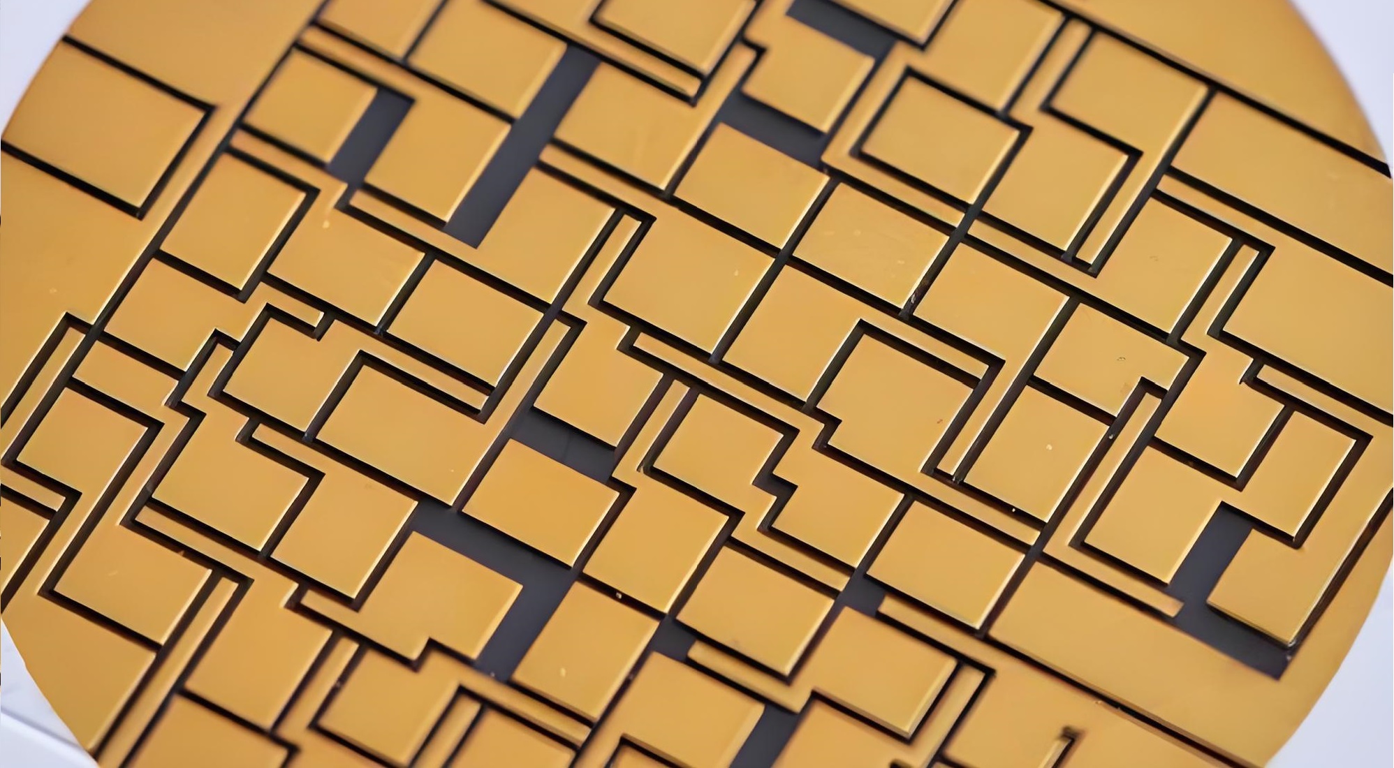
What Is a Ceramic Substrate PCB?
A ceramic substrate PCB is a circuit board made using ceramic materials as the base instead of traditional resins. Unlike FR-4 or other standard materials, ceramics offer excellent heat resistance, thermal conductivity, and mechanical strength.
They’re not just tough—they’re smart. Ceramics can carry high-frequency signals without distortion. They also handle high power loads with ease, which is why they’re often used in power modules and high-speed communication systems.
Ceramic Substrate PCB Types
Ceramic PCBs vary based on two main categories: materials and production techniques.
1. Divided by Materials
- Aluminum Nitride (AlN) PCB
Aluminum nitride PCB is favored for its exceptional thermal performance. Its thermal conductivity ranges from 170 to 230 W/m·K, which is much higher than FR4 or even alumina. It’s often used in power devices, RF modules, and LED lighting. This type also provides strong insulation and good mechanical stability.
- Alumina (Al2O3) PCB
Alumina PCBs are the most common type. They offer a balanced mix of electrical insulation, mechanical strength, and cost-effectiveness. They’re available in 96%, 99%, or 99.6% purity levels. The higher the purity, the better the thermal and electrical properties. These boards are widely used in automotive sensors, LED lighting, and industrial controls.
- Beryllium Oxide (BeO) PCB
BeO PCBs offer the highest thermal conductivity among ceramic materials—up to 300 W/m·K. However, due to safety concerns during manufacturing, it’s less popular today. Still, for very specific military or aerospace projects, it’s an option. At Best Technology, we generally recommend safer materials like AlN or Alumina for most projects.
- Silicon Nitride (Si₃N₄) PCB
Silicon nitride offers high strength and fracture toughness. It handles heavy vibration and thermal shock better than others. It performs well in both high-temperature and high-load environments.
- Silicon Carbide (SiC) PCB
SiC gaining attention in high-demand environments like electric vehicles and aerospace systems. It offers thermal conductivity in the range of 80 to 180 W/m·K, along with excellent chemical and radiation resistance.
- Zirconia (ZrO₂) PCB
Zirconia is known for its toughness and wear resistance. ZrO₂ is used in environments requiring abrasion resistance, such as medical implants, aerospace sealing systems, or sensor housings. It’s not as popular for power electronics but fills special roles where durability matters more than heat dissipation.
2. Divided by Manufacturing Techniques
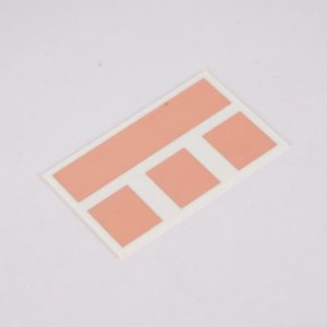
- Thick Film Ceramic Substrate PCB
These use screen-printing to apply conductive and dielectric pastes onto the ceramic surface. It’s reliable, cost-effective, and great for low to medium-volume production. The conductor is usually silver or gold. This type works well for sensors and power hybrid circuits. They also support multilayer designs.
- Thin Film Ceramic PCB
This method uses vacuum deposition and photolithography. It’s precise and supports very fine lines and spaces. Thin-film PCBs are more expensive but deliver unmatched performance in miniaturized devices, such as medical implants or RF modules.
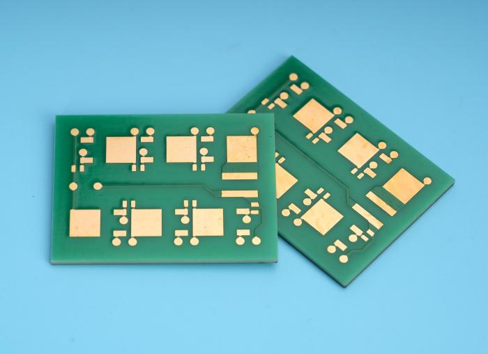
- DBC Ceramic PCB (Direct Bonded Copper)
DBC PCBs bond copper directly onto a ceramic surface through a high-temperature process. The copper layer is thick and can carry high currents. They are suitable for power semiconductors and automotive applications. They also offer strong adhesion and excellent heat spreading.
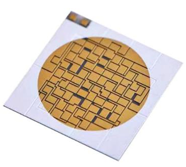
- DPC Ceramic PCB (Direct Plated Copper)
DPC PCBs are made by plating copper directly onto the ceramic using a chemical process. They can achieve finer features than DBC and are suitable for high-frequency or miniaturized devices.
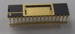
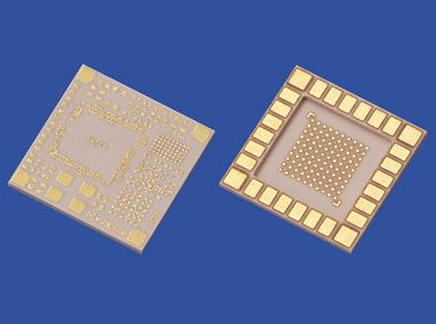
- HTCC Ceramic PCB (High-Temperature Co-fired Ceramic)
HTCC involves firing a mix of ceramic and metal powders at over 1600°C. It’s durable and works in harsh environments. HTCC PCBs are commonly used in military and aerospace industries due to their stability under extreme conditions.
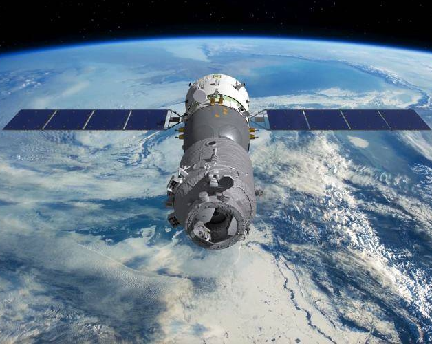
- LTCC Ceramic PCB (Low-Temperature Co-fired Ceramic)
LTCC is similar to HTCC but fired at a lower temperature (around 850°C). This process allows for the embedding of passive components, which saves space. It’s perfect for compact, multi-functional devices, especially in telecom and satellite systems. Both HTCC and LTCC ceramic substrate can made into multilayers.
- AMB Ceramic PCB (Active Metal Brazing)
AMB PCBs use an active brazing technique to bond copper and ceramic. This method provides better bonding strength than DBC and is ideal for high-load applications like electric vehicles.
Technical Specification of Beryllium Oxide (BeO) Ceramic Substrate
| Material Property | Unit | Value | |
| Color | \ | White | |
| Medium grain size | um | 3-5 | |
| Surface roughness (Ra) | um | 0.3-0.5 | |
| Density | Kg/m3 | 3010 | |
| Rate of water absorption | % | 0 | |
| Bending strength | 4 point method (40x4x3mm3) | Mpa | 400 |
| Dual ring method (0.63mm substrate thickness) | Mpa | 500 | |
| Thermal conductivity (20-100℃) | W/m-k | 220-250 | |
| Specific heat | J/kg.K | 800 | |
| Coefficient of Linear expansion | 1*E-6 / K | 5.1-8.9 | |
| Dielectric constant | 6-7 | ||
| Dielectric loss factor (1 MHz) | 1*E-3 | 0.3 | |
| Breakdown Voltage | 2.0mm substrate | KV/mm | 34 |
| 1.0mm substrate | 17 | ||
| 0.635mm substrate | 11 | ||
| Volume resistivity | 20℃ | Ohm * cm | – |
Technical Specification of Silicon Nitride (Si₃N₄) Ceramic Substrate
| Material Property | Unit | Value | |
| Color | \ | Gray, White, Off-White | |
| Medium grain size | um | 3-5 | |
| Surface roughness (Ra) | um | 0.3-0.5 | |
| Density | Kg/m3 | 3120-3220 | |
| Rate of water absorption | % | 0 | |
| Bending strength | 4 point method (40x4x3mm3) | Mpa | 147 |
| Dual ring method (0.63mm substrate thickness) | Mpa | 490 | |
| Thermal conductivity | W/m-k | 18.42 | |
| Specific heat | J/kg.K | 710 | |
| Coefficient of Linear expansion (20-1000℃) | 10-6/℃ | 2.8-3.2 | |
| Dielectric constant | 9.4-9.5 | ||
| Dielectric loss factor (1 MHz) | 1*E-3 | 0.3 | |
| Breakdown Voltage | 2.0mm substrate | KV/mm | 34 |
| 1.0mm substrate | 17 | ||
| 0.635mm substrate | 11 | ||
| Volume resistivity | 20℃ | Ohm * m | 1.4*105 |
| 500℃ | Ohm * m | 4*108 | |
Technical Specification of Silicon Carbide (SiC) Ceramic Substrate
| Material Property | Unit | Value | |
| Color | \ | Black | |
| Medium grain size | um | 3-5 | |
| Surface roughness (Ra) | um | 0.3-0.5 | |
| Density | Kg/m3 | 3220 | |
| Rate of water absorption | % | 0 | |
| Bending strength | 4 point method (40x4x3mm3) | Mpa | 400 |
| Dual ring method (0.63mm substrate thickness) | Mpa | 500 | |
| Thermal conductivity | W/m-k | 83.6 | |
| Specific heat | -106℃ | J/kg.K | 399.84 |
| 107℃ | 472.27 | ||
| 247℃ | 1266.93 | ||
| Coefficient of Linear expansion (20-1000℃) | 10-6/℃ | 6.28-9.63 | |
| Dielectric constant | 7 | ||
| Dielectric loss factor (1 MHz) | 1*E-3 | 0.3 | |
| Breakdown Voltage | 2.0mm substrate | KV/mm | 34 |
| 1.0mm substrate | 17 | ||
| 0.635mm substrate | 11 | ||
| Volume resistivity | 20℃ | M * cm | 102 |
Technical Specification of Zirconia (ZrO₂) Ceramic Substrate
| Material Property | Unit | Value | |
| Color | \ | White | |
| Medium grain size | um | 3-5 | |
| Surface roughness (Ra) | um | 0.3-0.5 | |
| Density | Kg/m3 | 5850 | |
| Rate of water absorption | % | 0 | |
| Bending strength | 4 point method (40x4x3mm3) | Mpa | 380 |
| Dual ring method (0.63mm substrate thickness) | Mpa | 500 | |
| Thermal conductivity | W/m-k | 2.09 | |
| Specific heat | J/kg.K | 563.89 | |
| Coefficient of Linear expansion (20-1000℃) | 10-6/℃ | 6.5-11.2 | |
| Dielectric constant | 27 | ||
| Dielectric loss factor (1 MHz) | 1*E-3 | 0.3 | |
| Breakdown Voltage | 2.0mm substrate | KV/mm | 34 |
| 1.0mm substrate | 17 | ||
| 0.635mm substrate | 11 | ||
| Volume resistivity | 1000℃ | Ohm * cm | 104 |
| 1700℃ | Ohm * cm | 6-7 | |
For technical specifications of Al2O3 and AlN, please click here to view the details.
What Is the Difference Between Ceramic Substrate and FR-4?
| Property | Ceramic Substrate PCB | FR-4 PCB |
| Material Composition | Inorganic (e.g., Al₂O₃, AlN, Si₃N₄) | Organic (Epoxy resin + fiberglass) |
| Thermal Conductivity | High (AlN: 170–230 W/m·K, BeO: up to 300 W/m·K) | Low (~0.3–0.5 W/m·K) |
| Operating Temperature | Up to 800°C or more | Limited to ~130–150°C |
| Electrical Insulation | Excellent and stable | Moderate |
| Dielectric Constant | Low and stable (AlN ~8.5, Al₂O₃ ~9.8) | Higher and less stable (~4.2–4.8) |
| Moisture Absorption | None (non-porous) | Yes (hygroscopic) |
| Mechanical Strength | High (brittle but rigid) | Good flexibility and toughness |
| Thermal Expansion (CTE) | Very low (~5–7 ppm/°C) | Higher (~14–17 ppm/°C) |
| RF / Microwave Performance | Excellent (low loss, stable dielectric) | Poor to average (higher signal loss) |
| Price | Higher | Lower |
| Application | Focus High-power, high-reliability systems (LEDs, lasers, RF) | General-purpose, consumer electronics |
| Design Flexibility | Less flexible, requires precise processing | Very flexible, supports complex multilayer structures |
How Thick Is a Ceramic Substrate?
Ceramic substrate PCBs come in various thicknesses, depending on the material and application. The most commonly used thicknesses range from 0.25 mm to 3.0 mm. However, special requests can push this range even further.
- For alumina, the standard thicknesses are 0.25 mm, 0.38 mm, 0.5 mm, 0.635 mm, 1.0 mm, and 1.5 mm. These sizes work well for LED packages and power control boards.
- Aluminum nitride substrates are typically used in 0.38 mm to 1.0 mm thicknesses. The thinner sheets are used in RF circuits, while thicker ones help in thermal management and mechanical support.
- Silicon nitride and silicon carbide can also be customized in terms of thickness. Some high-strength applications require boards thicker than 2 mm to add mechanical stability.
- For LTCC and HTCC processes, the thickness can vary as layers are stacked. After sintering, the final board may be thinner than expected due to shrinkage. Designers often specify individual layer thicknesses from 100 µm to 300 µm before lamination.
Factors Affect Ceramic Substrate PCB Price
A ceramic substrate price can be varied depends on the material and process used. Here is a detailed explanation.
1. Material Type
Alumina is the most cost-effective, followed by aluminum nitride. Silicon nitride, silicon carbide, and beryllium oxide are more expensive due to material costs and production challenges.
2. Board Size and Thickness
Larger boards cost more to produce. Thicker substrates also require more raw material and longer sintering times, increasing the cost.
3. Layer Count
Single-layer ceramic PCBs are cheaper. Multilayer designs need more lamination and alignment, raising both time and processing costs.
4. Metallization Method
The choice between thick film, DPC, DBC, or HTCC has a big impact. DPC and DBC processes require specialized equipment, so they are more expensive than thick film types.
5. Tolerances and Precision
If your application requires tight tolerances or fine trace widths, this will increase the cost. More precise laser cutting, printing, or etching takes longer and demands higher quality control.
6. Volume
Like most products, higher quantities reduce the per-unit cost. Low-volume or prototype runs are usually priced higher due to tooling and setup.
7. Surface Finish and Testing
Optional services such as ENIG, silver plating, or 100% electrical testing will raise the overall price.
In summary, the price of a ceramic substrate PCB depends on the complexity, material, and quality requirements. While they cost more than FR-4 boards, their performance and longevity often justify the higher investment.
What Is a Ceramic PCB Used For?
- High-brightness and long-lifetime lighting
- Inverters
- IGBTs
- Motor drives
- Imaging systems
- Implants
- Diagnostics
- Telecom
- Antennas
- Filters
- Base stations
- EV batteries
- Sensors
- Control units
- Aerospace
- Radar systems
- Satellite modules
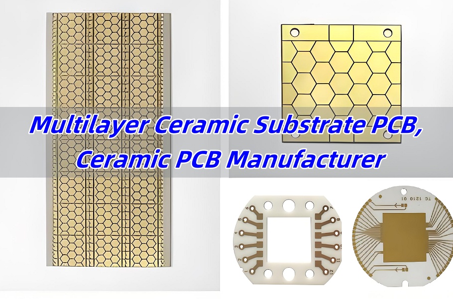
Multilayer Ceramic PCB Manufacturing Process
Multilayer ceramic PCBs are built using different methods than traditional FR-4 boards. The most popular technique is the thick film, HTCC or LTCC process, which allows stacking multiple ceramic layers with embedded circuits. Here’s a step-by-step look at how they’re made:
1. Ceramic Tape Casting
First, thin ceramic tapes (called green sheets) are cast using alumina, aluminum nitride, or other ceramic powders mixed with binders and solvents. These tapes are then dried and punched to create holes for vias.
2. Via Filling and Screen Printing
Vias are filled with conductive pastes such as gold, silver, or tungsten. Then, a conductive pattern is printed on each layer using screen printing or sputtering techniques.
3. Layer Alignment and Lamination
Multiple layers are stacked together carefully, with precise alignment. They are then laminated under pressure and heat, forming a compact structure ready for sintering.
4. Sintering or Firing
In this step, the laminated structure is fired in a high-temperature furnace—up to 1,600°C for HTCC or 850°C for LTCC. This burns off the organic materials and solidifies the ceramic and metal layers.
5. Metallization and Plating
After sintering, the external layers are coated with surface finishes like silver, gold, ENIG, or nickel. These finishes improve solderability and prevent oxidation.
6. Laser Cutting and Drilling
Final shaping is done using CO₂ or UV lasers. This step defines the board outline and makes precise holes for connectors or mounting.
7. Inspection and Testing
Each board undergoes dimensional inspection, electrical testing, and sometimes X-ray analysis to check for internal defects or misalignments.
Why Choose Best Technology as Your Ceramic PCB Manufacturer?
You’re not just buying a board. You’re choosing a partner. At Best Technology, we offer:
- Free ceramic substrate technical consultation
- In-house production for better lead times
- 100% electrical testing before shipping
- Rapid prototyping and mass production
- Custom designs for all industries
- Friendly support team that speaks your language
- Military-grade quality
- ISO13485, IATF16949, AS9100D certificated
- No minimum order quantity requirement
- 5 years quality assurance
Let us help bring your next high-performance product to life. Whether it’s Aluminum Nitride PCB, Alumina, or multilayer ceramic PCB, we’re ready to deliver results you can count on.