What is a Microvias?
A microvia is a small hole drilled into a PCB that connects different layers. They are essential for high-density interconnections and are commonly used in advanced electronic designs. Typically, microvias equal to or less than 150 microns drilled on the PCB board with a laser. In 2013, the IPC standard changed the definition of microvias to those with an aspect ratio of 1:1. Ratio of aperture to depth (not exceeding 0.25mm). Previously, micropores were less than or equal to 0.15 mm in diameter, so they typically spanned only one layer.
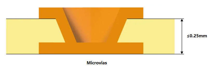
Because the diameter is very small compared to mechanically drilled through holes (PTH), we define them as microvias, usually connecting only one layer of the board to its adjacent layers. These through holes reduce the possibility of any type of manufacturing defect because they are laser drilled, thus reducing the possibility of any residue remaining after the process. Because of their small size and ability to connect one layer to the next, they can make dense printed circuit boards with more complex designs.
Types of Microvias
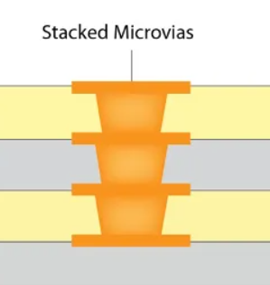
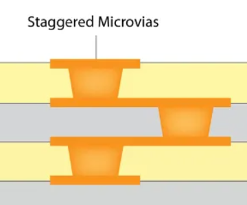
There are two types of microvias in the PCB design – stacked microvias and staggered microvias.
- Stacked Microvias
Stacked microvias are formed by stacking multiple layers on top of each other to provide a path through which current flows. Create a hole in one layer and drill into another layer below. The top layer is welded or welded to the bottom layer to form an interconnect between the two layers. This allows for fast, efficient routing without compromising performance or reliability.
- Staggered Microvias
The interlaced microvias is aligned with the pad of the same layer, but is offset from its center by half of the pad diameter. The distance from its center to the edge of the board is also half the diameter of the pad. Staggered microvias allow you to place two through holes in a single pad without overlapping them or having to route wires on different layers together in this location. This type of microvias can be used for electrical connections to the surrounding brass pads and traces.
What is the Difference Between Vias and Microvias?
Vias and microvias serve similar purposes in connecting different layers of a PCB, but they differ significantly in size and application.
1. Size
One of the most significant differences between vias and microvias is their size. Standard vias typically have a diameter greater than 150 micrometers (μm), while microvias are defined as having a diameter of 150 μm or less.
2. Design Complexity
As technology advances, the demand for higher circuit densities and more complex designs has grown. Microvias enable designers to create intricate multilayer circuits that were not possible with standard vias.
3. Layer Connection
Standard vias can connect any number of layers in a PCB, typically running from the outer layer through to the inner layers. In contrast, microvias are usually used for connecting one or two layers. Microvias are commonly employed in multilayer PCBs, where they can connect the outer layer to one or more inner layers without passing through the entire board.
4. Aspect Ratio
The aspect ratio, which is the ratio of the depth of a via to its diameter, is another important difference. Standard vias generally have lower aspect ratios, making them easier to fabricate. Microvias, due to their smaller size, often have higher aspect ratios. A typical aspect ratio for microvias ranges from 1:1 to 2:1.
5. Applications
Standard vias are commonly used in traditional PCB designs for applications where space is not as critical. They are suitable for general-purpose circuits, power distribution, and less complex layouts. In contrast, microvias are essential in high-density applications, such as smartphones, tablets, and advanced computing devices, where compact designs are necessary.
Microvias vs. Blind Via
Blind vias connect the outer layer of the PCB to one or more inner layers without penetrating the entire board. As the name suggests, these through-holes are “blind holes” because they are not visible from the other side of the PCB. Blind holes have several advantages, such as saving space on the board, enabling a more compact design, and improving signal integrity by reducing the length of the signal path.
The blind via passes through the surface layer of the PCB, extending through only a portion of the board to connect the surface layer to one or more inner layers. They are a key component in current PCB designs, allowing surface components to connect to inner layers while minimizing the number of layers required for wiring. The advantages of using blind vias including:
- Increased density
- Reduce the number of layers
- Improved signal performance
- Good for heat dissipation
- Improve mechanical strength
Can Microvias be Designed in Multilayer MCPCB?
Yes, microvias can indeed be designed in multilayer MCPCBs. In fact, their small size and efficient design make them ideal for these types of boards. Multilayer MCPCBs often require compact interconnections to accommodate various functionalities, and microvias facilitate this need. By enabling multiple layers to connect efficiently, microvias enhance the overall performance of the MCPCB. Additionally, they contribute to improved thermal management, a critical factor in high-power applications. Their integration in multilayer designs is a significant advantage for modern electronics.
The process for using microvias in multilayer metal-based circuit boards includes the following key steps:
1. Inner laser drilling and plating: This is the first step in the production of microvias, precisely drilled by laser technology, and electroplated.
2. Resin filled: The micro-vias after electroplating are filled with resin to enhance the stability of the structure.
3. Resin grinding: Grind the orifice after the jack hole to ensure a smooth surface.
4. Electroplating: Metallize the surface of the orifice resin to achieve electrical interconnection between layers.
5. Inner circuit etching and outer layer lamination: To complete the production of the inner circuit, and the outer layer of laser drilling and graphic plating, and finally realize the production of multi-layer circuit board.
MCPCB Material in EBest Circuit (Best Technology)

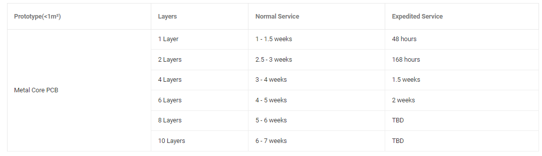
MCPCB Prototype Lead Time (Vary Depends on the MCPCB Design)