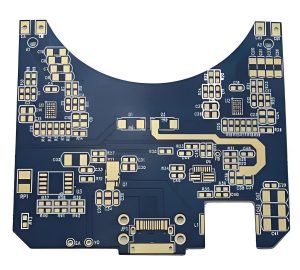
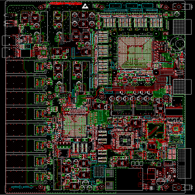
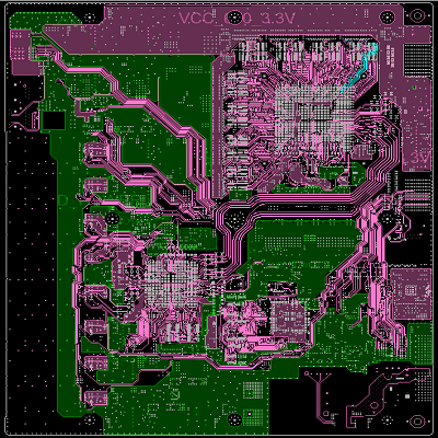
Best technology offers numerous PCB design solutions for our customer, from HDI design, high speed device PCB design, AI optical module design and network motherboard design for network switching. Below is one of our network motherboard design solutions:
An ATCA network switching motherboard
[1]:BCM88XXX, BCM55XXX chips
[2]:60A maximum current
[3]:8口10G optical network
[4]: 8 x DDR3 chips
Network Switching Differential Pair Design Guide
- Each TrxP/TrxN signal group (where xcx0-3) shall be routed as a differential pair. This includes the entire length of wiring processing.
- The individual differential correspondences are packed together as tightly as possible. Impedance calculations are usually started by selecting the smallest line blank (4-5mil). The tracking width is then adjusted to achieve the necessary impedance.
- Differential line group resistance of Ethernet is calculated at 100 ohms.
- In general, when routing the four differential pairs of the Gigabit Ethernet to the r45 connector, at least one pair will pass through to the opposite outer layer.
- Priority should be given to differential pair wiring. Terminals should be added after the routing is determined
- The values of all resistance terminals in the Ethernet front end should be 1.0% tolerance
- All capacitor termination Ethernet front ends in the module should have strict tolerances and high quality product media (npo)
You are welcome to contact us if you want to get your DIY network switching PCB designs.