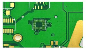
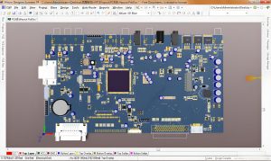
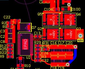
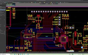
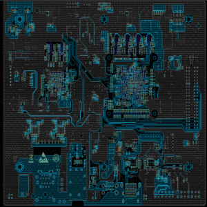
PCB design is an indispensable part of modern electronic product development. An efficient and reliable PCB design can ensure the normal operation of the circuit and meet the performance and manufacturability requirements of the product.
PCB design (Printed Circuit Board Design) refers to the design of circuit boards using electronic design automation software (EDA), designing the layout and circuit connections of printed circuit boards (PCBs). Circuit boards are an important part of electronic products. They can connect electronic components together and transmit signals through wires.
Is PCB design hard to learn?
PCB design is not difficult to learn. The key lies in mastering the relevant basic knowledge and practical experience.
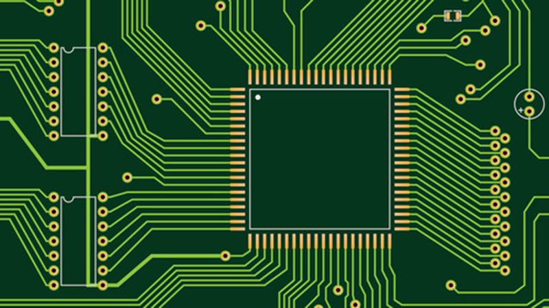
PCB design mainly involves electronic circuit knowledge and software operation skills. For people with electronic circuit foundation, it is relatively easy to learn the use of PCB design software. It is important that learners should use their spare time to learn and practice at the same time. They can assist in learning by watching video tutorials. These resources can help understand the basic concepts and skills of circuit design and software operation.
In addition, the difficulty of PCB design lies mainly in the design of wiring rules, which is the most complex and critical part of PCB design. Beginners should pay attention to the design of conventional constraint rules, such as the size of vias, line width and line spacing, etc., which need to be mastered through practical operation and practice. Just reading materials is not enough. Practical operation and practice are the key to improving PCB design capabilities.
In general, although PCB design involves certain technical difficulties, it can be gradually mastered through systematic learning and practice.
What should I learn before PCB design?
Before PCB design, you need to learn the following key knowledge and skills:
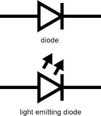
1. Basic knowledge reserve: First of all, you need to understand various electronic components, such as resistors, capacitors, inductors, diodes, triodes, integrated circuits, etc. You also need to be familiar with common circuit topologies, such as amplifier circuits, filter circuits, oscillation circuits, and their functions and representation methods in circuits.
2. PCB design software: Be proficient in at least one PCB design software for schematic design, component layout, wiring, and generation of PCB production files, such as Altium Designer, EAGLE, PADS, OrCAD, etc.
3. Circuit board manufacturing process: Understand the manufacturing process of PCB circuit boards, including substrate material selection, circuit pattern transfer, etching, drilling, welding, assembly, etc.
4. Component packaging: Familiar with the packaging types and sizes of various components, such as DIP, SOP, QFP, BGA, etc., as well as their characteristics and usage scenarios.
5. Basic terms and concepts: Master some basic PCB terms, such as microstrip, stripline, differential line, via, solder mask, silk screen, structural diagram, etc.
6. Circuit function and signal flow: Understand the function and signal flow of the circuit, and be able to distinguish between digital circuits and analog circuits, as well as places with large and small currents.
By mastering the above knowledge and skills, you can better design and layout circuits, improve the performance and reliability of circuit boards,
Which software is used for PCB design?
1. Altium Designer is a powerful PCB design software that provides a wealth of tools and libraries to quickly create complex circuit board designs. This software has an intuitive interface and powerful simulation functions to help designers quickly verify the correctness of the design. It also supports multiple design file formats, which is convenient for collaboration with other design tools.
2. Cadence Allegro is a comprehensive circuit board design software with powerful layout and routing tools, as well as multiple simulation and verification tools to ensure the correctness of the design. It also supports multiple design file formats for team collaboration.
3. Mentor Graphics DesignX is also a powerful PCB design software that provides a variety of tools and libraries to help designers quickly create complex circuit board designs. It also has an intuitive interface and powerful simulation functions, and supports multiple design file formats.
4. PADS is a professional circuit board design software with powerful layout, routing, simulation and verification functions, which can quickly complete complex PCB design work. It also supports multiple design file formats, which is convenient for collaboration with other design tools.
These software are all commonly used PCB design tools with powerful layout, routing, simulation and verification functions, which can help designers quickly complete complex PCB design work.
What is the basic rule of PCB design?
The basic rules of PCB design involve many aspects, including layout, routing, power and ground design, signal integrity, etc.
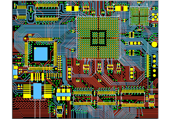
Follow the design principle of placing in a straight line along the signal flow direction to avoid the signal from circling back and forth to reduce the impact of direct signal coupling.
The filtering, protection and isolation devices of the interface circuit should be placed close to the interface to achieve effective protection, filtering and isolation effects.
For high-speed signals or high-current signals, multi-layer board design should be considered to control the signal loop area.
2. Wiring rules:
Control the length of the trace, especially for important signal lines, such as clock signals, the trace length should be shortened as much as possible to reduce unnecessary interference.
Avoid forming self-loop traces to reduce radiation interference.
Follow the principle of minimum ground loop, design the signal line and its loop to form the smallest possible loop area to reduce external radiation and external interference.
3. Power and ground design:
The power plane should be retracted a certain distance relative to its return ground plane to effectively suppress edge radiation problems.
Avoid overlapping of different power layers in space to reduce interference between different power supplies.
4. Drawing:
When drawing the board frame, a specific line width should be used to ensure that the error between the board frame size and the assembly size is within the allowable range.
Set a reasonable origin to ensure that the coordinates of the SMT original are within the first quadrant.
Set a prohibited area, especially prohibiting routing and placing components within a certain range around the mounting hole.
Following these basic rules can ensure the effectiveness and reliability of PCB design, while improving product performance and user experience.
How long does it take to design a PCB board?
It takes about 1-2 days to design a PCB board, and the specific time depends on multiple factors, including the number of layers of the PCB, design complexity, etc.
Number of layers and complexity: The more layers the PCB has, the more complicated the design process is, and more time and delicate work are required to ensure the correctness and performance of the circuit.
Design stage: PCB design includes multiple steps such as design layout, schematic drawing, and PCB design conversion.
The time to design a PCB board is a comprehensive estimate involving multiple stages and factors.
What is the proper PCB layout?
Proper PCB layout involves many aspects, including structural requirements, heat dissipation considerations, component spacing, routing rules, etc.
Structural requirements: First, the PCB layout must meet the structural requirements, including the location arrangement of structural components such as power sockets and DVI interfaces.
Heat dissipation considerations: The distribution of heat sinks should be even to ensure good ventilation of the air path. Avoid heat sinks blocking the air path to avoid affecting the heat dissipation effect.
Component spacing: Capacitors, ICs, etc. should be kept away from thermal components to avoid being affected by heat.
Routing rules: The design of the current loop should consider the convenience of threading, and the lead hole spacing should not be too far or too close. The layout of input/output and AC/socket should meet the consistency of the length of the two lines, leaving a certain space margin, and pay attention to the position of the plug wire buckle and the convenience of plugging and unplugging.
Special component layout: For high-frequency components and components with high potential difference, the distance between them should be increased to avoid electrical interference and damage.
Wiring design parameters: including the line width of the copper trace, the minimum gap between the copper foil traces, the minimum distance between the copper foil traces and the edge of the PCB board, etc. .
In summary, the correct PCB layout is a process that comprehensively considers the structure, heat dissipation, component spacing, routing rules and wiring design parameters, aiming to optimize the performance and reliability of the circuit board.
Conclusion:
Designing a PCB board is a complex and meticulous process involving multiple steps and considerations. Systematically complete the design process of a PCB board. Each step requires careful operation and multiple checks to ensure the quality and reliability of the final product. BEST Technology’s PCB designers have many years of design experience and are far ahead in the industry design. We can meet any PCB design you need.


