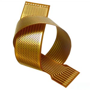
PCB copper thickness is one of the most important parts of a printed circuit board’s design. It directly affects how much current your board can carry, how it dissipates heat, and how strong the overall structure is. Therefore, whether you’re working on a high-current power supply or a compact signal board, understanding the copper layer’s thickness plays a key role in avoiding costly design mistakes.
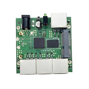
At Best Technology, we focus on both manufacturing and sales services for various types of printed circuit boards and PCB assembly. To guarantee quality, our PCBs undergo strict tests like X-ray, 3D AOI (Automated Optical Inspection), and 3D SPI (Solder Paste Inspection) to ensure flawless performance even in extreme environments. Moreover, Best Technology offers a fast and reliable 72-hour PCB prototype turnaround with free DFM feedback. In addition, our production lead times are 30% faster than the industry average, helping you meet tight deadlines with ease.
If you need urgent order coordination or have any questions about PCB copper thickness or PCB copper thickness tolerance, please feel free to reach out directly to our team at sales@bestpcbs.com. We’re always ready to support your project needs.

How thick is PCB board FR4 copper?
When people talk about standard PCBs, FR4 is the core material they usually mean. In most cases, the copper thickness on FR4 boards depends on the design, but generally, the most common one used is 1 oz copper.
To explain further, 1 oz copper means the copper layer weighs one ounce per square foot. That equals 35 microns or 1.4 mils in thickness. Even so, manufacturers can offer a wide range—from 0.5 oz to 3 oz, or even more—based on specific customer needs.
In typical applications, most 2-layer and 4-layer FR4 boards use 1 oz as the default. However, for power circuits that demand more robust current handling, 2 oz or 3 oz copper is often the better choice.
What is the standard thickness of a copper layer on a PCB?
The standard PCB copper thickness is 1 oz (35 µm). But this can change depending on the application. Some high-density boards may use 0.5 oz (17.5 µm) to save space. On the other end, power boards can go with 2 oz (70 µm) or more.
Here’s a quick reference:
- 0.5 oz = 17.5 µm
- 1 oz = 35 µm
- 2 oz = 70 µm
- 3 oz = 105 µm
You’ll often see this in a pcb copper thickness chart or a pcb copper thickness table provided by PCB fabricators. It’s always a good idea to check with your supplier before starting your design.
How thick is 1 oz copper on a PCB?
This is one of the most searched questions online. 1 oz copper thickness in mm is 0.035 mm. In inches, it equals around 0.0014 inch. If you’re using a pcb copper thickness calculator, this will be the default thickness unless you change it.
The good part about 1 oz copper is its balance. It works for most signal and low-power designs. It’s also easy to etch and doesn’t raise costs too much. Need more current? Then jump to 2 oz or thicker copper.
What is the difference between 1 oz and 2 oz copper PCB?
Let’s compare them quickly:
- 1 oz copper = 35 µm
- 2 oz copper = 70 µm
With 2 oz copper, your board can carry more current and handle more heat. This is good for power supply circuits, motor drivers, and high-load designs.
However, thicker copper may need wider spacing and larger traces. That’s why it’s important to check design rules before switching.
You can use a PCB copper thickness vs current chart or a PCB copper thickness current calculator to find out the max current your traces can handle.
What is the thickness tolerance of copper in PCB?
Manufacturers follow industry standards, but there’s always some tolerance in pcb copper thickness. This tolerance depends on the copper weight and the etching process.
Usually, the tolerance is:
- ±10% for 0.5 oz and 1 oz
- ±15% for 2 oz or higher
So, a 1 oz copper layer might actually range from 31 µm to 39 µm. These differences can matter in tight power designs. It’s smart to ask your supplier for exact specs if your project is sensitive to trace width or heat.
What’s the difference between PCB copper thickness in oz, mm, and inches?
People often get confused because copper thickness is shown in many units. Here’s how to convert oz to mm or inches:
| Oz (ounce/ft²) | Microns (µm) | Millimeters (mm) | Inches |
| 0.5 oz | 17.5 µm | 0.0175 mm | 0.0007” |
| 1 oz | 35 µm | 0.035 mm | 0.0014” |
| 2 oz | 70 µm | 0.070 mm | 0.0028” |
| 3 oz | 105 µm | 0.105 mm | 0.0041” |
For less common options like 1/2 oz copper thickness in mm or 1/3 oz copper, the rule is the same—divide the value based on 1 oz.
How to calculate PCB copper thickness accurately?
To get a more precise idea of the copper layer, you can use a pcb copper thickness calculator. Some calculators also let you estimate the weight, trace width, and current carrying ability based on copper thickness.
For weight, you can use a pcb copper weight calculator if you need to know the total copper mass for large-volume production or thermal analysis.
These tools are especially useful when designing multilayer PCBs with different copper thicknesses on different layers.
How to check PCB copper thickness?
There are three main ways:
- Ask the supplier – Most PCB makers include copper thickness in their stack-up files.
- Check the fab drawing – Often marked as 0.5 oz, 1 oz, etc., on each layer.
- Use physical testing – Some advanced users measure thickness using a micrometer or microscope after etching.
Still, for most users, trusting your fabricator’s data is good enough. Just make sure to request the thickness you need in your Gerber or fabrication notes.
In conclusion, choosing the right PCB copper thickness isn’t just a number game. It can impact the heat flow, voltage drop, size of the board, and even reliability over time. That’s why understanding copper thickness is one of the smart ways to make your design work better from the start.
At Best Technology, we help you make the right decision for your design. Whether you’re working on high-frequency boards or heavy copper PCBs for power electronics, we have the experience and tools to support you. You can get the services like:
- Request custom copper thickness for any layer.
- Use our support to optimize trace width based on current needs.
- Get a free consultation on stack-up and copper weight.
When you choose us, you’re not just buying a PCB. You’re getting a trusted partner in the entire process. Ready to build better boards with the right copper thickness? Warm welcome to reach out to Best Technology at sales@bestpcbs.com and get a best quote that matches your exact design needs.