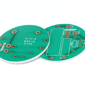
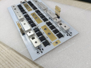
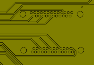
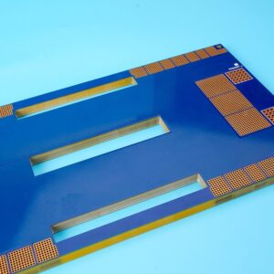
PCB copper traces are copper wires used to conduct current and signals on PCBs. They are usually etched from copper foil and have a specific width and thickness. The design of copper traces needs to consider factors such as current carrying capacity, signal integrity, and heat dissipation performance. They are widely used in various electronic devices to connect components and transmit electrical signals.
What is copper trace in pcb?
A copper trace in PCB is essentially a flat, conductive pathway formed on the PCB’s surface. This pathway connects the different components of the board, allowing electrical signals or power to flow between them.
Copper traces are created by etching copper foil, which is typically laminated onto a non-conductive substrate (such as FR4 or other materials).
The design and size of copper traces can significantly impact the performance of the PCB. These traces are precisely engineered to handle specific electrical loads, ensuring the efficient functioning of the PCB in devices such as smartphones, computers, automotive systems, medical equipment, and much more.
What is the role of copper trace in pcb design?
The role of copper trace in PCB design is to provide a reliable and efficient pathway for electrical current. Copper, due to its high conductivity, ensures that the signal or power transmitted through the PCB travels with minimal loss.
The width and thickness of copper traces, as well as their routing, need to be carefully designed to match the required current-carrying capacity and to prevent issues such as overheating, signal interference, and voltage drops.
In PCB design, copper traces serve as the arteries of the board. They ensure that electrical signals flow smoothly from one component to another. Without properly designed copper traces, the performance and reliability of the entire circuit can be compromised, leading to malfunctioning or inefficient devices.
What factors affect copper trace design?
Several factors influence the design of copper traces in PCB manufacturing. The key considerations include:
- Current Carrying Capacity: Copper traces must be designed to handle the amount of current they will carry. If the trace is too narrow, it may overheat and cause damage to the board or components.
- Trace Length: Longer traces have more resistance, which can cause signal degradation or voltage drops. It’s essential to minimize trace length where possible to reduce these effects.
- Trace Width: The width of the copper trace directly affects its current-carrying capacity. A wider trace can carry more current without overheating, but it may take up more space on the PCB.
- Temperature: High temperatures can affect the performance of copper traces, causing them to expand or degrade. Proper thermal management is essential to ensure that copper traces continue to function efficiently.
- Board Thickness and Material: The thickness of the PCB substrate and the copper layer can affect the trace’s resistance and heat dissipation. Different materials have different thermal conductivity, which should be considered during the design phase.
- Signal Integrity: For high-speed circuits, the design of the copper trace must minimize electromagnetic interference (EMI) and crosstalk between adjacent traces.
How does copper trace width affect pcb performance?
The width of copper traces is one of the most critical design parameters in PCB layout. Trace width affects several factors, including:
- Current Carrying Capacity: Wider copper traces have a higher current-carrying capacity, meaning they can safely handle larger electrical loads without overheating. Narrower traces are more prone to heating under higher currents, which can lead to failure.
- Power Dissipation: As current flows through a copper trace, some of the electrical energy is converted into heat due to the resistance of the trace. Wider traces help distribute heat more effectively, reducing the risk of thermal damage to the board.
- Signal Integrity: The width of the trace can also influence the impedance of the signal. Incorrect trace width can cause reflections, signal loss, or noise in high-speed circuits.
- Size and Space Optimization: While wider traces carry more current, they also take up more space on the PCB.
PCB line width and current carrying capacity
The current carrying capacity of a copper trace is a key factor in determining its appropriate width. Wider traces can carry more current without excessive heating, while narrower traces are limited in the amount of current they can handle before becoming too hot.

In general, the higher the current, the wider the trace needs to be. However, in designs where space is limited, other solutions such as multi-layer PCBs or increasing copper thickness can also help meet current-carrying requirements without significantly increasing trace width.
How do you calculate pcb trace width?
To calculate PCB trace width, designers need to take into account several parameters:
- Current: The amount of current the trace will carry.
- Temperature Rise: The maximum allowable temperature increase in the trace due to the current.
- Copper Thickness: The thickness of the copper layer used in the PCB.
- PCB Material: The thermal conductivity of the PCB material, which can affect the heat dissipation from the trace.
There are several online PCB trace width calculators that use formulas and standards (like IPC-2221) to calculate the appropriate trace width based on these parameters.
These calculators provide a quick and reliable way to ensure that your PCB design meets the current requirements without overheating or compromising signal integrity.
How do you calculate copper trace width for different currents?
When calculating copper trace width for different currents, the general approach is to increase the trace width as the current demand increases.
- Determine the Current: Start by determining the amount of current that the trace needs to carry. This will be based on the requirements of the components connected to the trace.
- Select Copper Thickness: Choose the copper thickness for the PCB. Standard copper thickness is typically 1 oz/ft² (which is 35 µm thick), but it can be increased for high-power applications.
- Calculate the Trace Width: Use a PCB trace width calculator or a standard formula to calculate the trace width required for the chosen current. The calculation takes into account the copper thickness and temperature rise constraints.
For instance, using a typical 1 oz/ft² copper PCB and a current of 2A, the required trace width for a 10°C temperature rise might be around 1.6mm. However, for a higher current like 5A, the trace width may need to be 3.4mm to safely carry the current without excessive heating.
Conclusion:
The width and design of the copper trace play a significant role in the PCB’s overall performance, impacting current carrying capacity, thermal management, and signal integrity.
If you need expert assistance in designing copper traces or any other aspect of PCB manufacturing, Best Technology is here to help. Contact us at sales@bestpcbs.com for top-notch PCB design and manufacturing services.


