Q: What is a PCB?
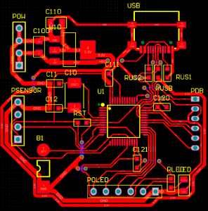
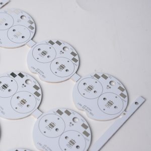
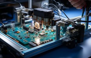
A: A PCB is used to mechanically support and electrically connect electronic components using conductive tracks, pads, and other features. It replaces bulky wiring by embedding copper traces directly onto a non-conductive board, which makes the circuit more compact, organized, and reliable. Unlike breadboards, which are used for prototyping, PCBs are permanent and more durable, reducing the chances of loose connections or accidental shorts.
Q: What are the basic layers of a PCB?
- Silkscreen
- Solder Mask
- Copper Layer(s)
- Substrate (FR4 or other material)
Q: What is a solder mask?
A: A protective layer preventing solder bridges and oxidation, leaving pads exposed.
Q: What is DFM (Design for Manufacturing)?
A: Designing PCBs to meet manufacturer capabilities (e.g., trace spacing, hole sizes, panelization).
Q: What is the standard thickness of a PCB?
Typically 1.6 mm (0.062 inches), but it can vary depending on the application.
Q: How do you design a PCB stackup?
A: Layer arrangement balancing signal integrity, power delivery, and cost (e.g., 4-layer: signal-ground-power-signal).
Q: What are basic checks when laying out an MCU-based design?
A: Ensure power traces are wide enough to carry current without voltage drops. Place the oscillator crystal or clock source close to the MCU pins to reduce noise and maintain clock integrity. Separate analog and digital ground areas and signals if the MCU uses both types of signals. Include bypass capacitors near power pins to filter noise.
Q: How do you handle mixed-signal layouts?
A: Separate analog/digital grounds, minimize cross-talk, and use shielding.
Q: What is the flow of a complete PCB design?
A: The full PCB design process involves multiple steps:
- Library Creation: Create symbols (schematic) and footprints (layout) for each component.
- Board Outline: Define the mechanical dimensions of the board.
- Netlist Import: Transfer the circuit connections from the schematic to layout software.
- Design Rules Setup: Define constraints like trace width, clearance, via sizes.
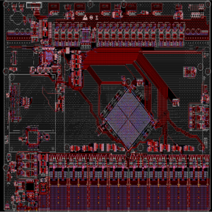
- Component Placement: Place components logically, optimizing for signal flow and accessibility.
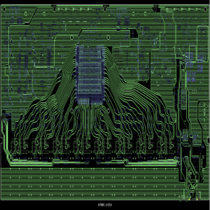
- Routing: Draw the copper traces to connect all components based on the netlist.
- Power/Ground Planes: Add split planes or solid fills for power and ground connections.
- Silkscreen & Assembly Layers: Add component labels and other printing layers.
- Gerber Generation: Output files needed by manufacturers to fabricate the board.
Q: What inputs are needed to design a PCB?
A: To design a PCB, you need:
- Schematic Diagram: The circuit blueprint.
- Bill of Materials (BOM): List of all components.
- Netlist: List of electrical connections.
- Board Outline: Mechanical boundary of the PCB.
- Mounting Hole Details: For mechanical assembly.
- Stackup Information: Defines how the board layers are arranged, especially important for complex designs.
Q: How do you verify schematic symbols or footprints?
A: Verifying schematic symbols and footprints is crucial to avoid errors in the final board. This involves cross-referencing the component’s datasheet to ensure pin configurations and dimensions match the footprint. You can print the footprint layout on paper and physically place the actual component over it to confirm accuracy. This step helps prevent costly rework or redesign later in the process.
Q: What is the 3W rule?
A: Spacing traces 3x the trace width apart to reduce crosstalk by ~70%.
Q: How do you place components?
A: Start by placing key components like connectors, microcontrollers, or BGAs (Ball Grid Arrays) that affect the overall layout. Follow the logical flow of the circuit and try to keep related components close together. Orientation and alignment should promote easy routing and good signal integrity.
Q: How do you place connectors?
A: Connectors should be placed at the edge of the PCB for easy access. Use right-angle connectors when the board needs to connect to other devices or enclosures. Always follow client or mechanical design guidelines regarding orientation and mechanical clearance.
Q: Why use decoupling capacitors?
A: Decoupling capacitors (also called bypass capacitors) are used to filter noise from the power supply lines. They help maintain a steady voltage by absorbing voltage spikes or dips. These capacitors should be placed as close as possible to the power pins of ICs to be most effective.
Q: If trace width increases, does its characteristic impedance increase or decrease?
A: When the trace width increases, the characteristic impedance decreases. This happens because a wider trace has higher capacitance and lower inductance, both of which reduce impedance.
Q: How to avoid high-frequency interference?
A: To reduce high-frequency interference:
- Keep analog and high-speed digital traces separate.
- Increase spacing between signal lines.
- Use ground guards (ground traces around sensitive lines).
- Avoid running high-speed traces over split planes.
Q: What are controlled impedance traces and where are they used?
A: Controlled impedance traces are designed with precise dimensions to maintain a specific impedance (e.g., 50Ω or 100Ω). They are used in high-speed digital circuits like USB, HDMI, and DDR.
Q: What is the skin effect in high-speed PCB design?
A: At high frequencies, AC current tends to flow on the surface of conductors. This reduces the effective conducting area and increases resistance, impacting signal integrity.
Q: What causes EMI in PCBs?
A: High-frequency signals, loop areas, improper grounding, and lack of shielding.
Q: How do you terminate transmission lines?
A: Use series, parallel, or AC termination to absorb signal reflections.
Q: How to route differential pairs?
A: Differential pairs should be routed with equal length and closely spaced to maintain constant differential impedance. The traces should run parallel, with no ground or power traces in between. Unequal lengths or inconsistent spacing can cause timing mismatches and degrade signal quality.
Q: How do you calculate the trace width for a given current?
A: Use IPC-2221 or IPC-2152 standards. Trace width calculator may save much time, like Best Technology’s free trace width & spacing calculator. Key variables affect the trace width include:
- Current
- Copper thickness
- Temperature rise
Q: Can matched resistors be added to differential pairs?
A: Yes, termination resistors (usually equal to the differential impedance) are added at the receiving end to absorb reflections and improve signal quality. This is especially important in high-speed data lines.
Q: What causes signal reflection?
A: Signal reflections happen due to impedance mismatches between traces and components. Reflections distort signals and can cause data errors. They are minimized using termination resistors, controlled trace geometry, and proper layer stackup.
Q: What is return current?
A: Return current is the path the current takes to return to the source. In PCBs, it usually flows through ground or power planes. High-speed signals tend to follow the path of least inductance, often right under the signal trace.
Q: How to optimize power distribution (PDN)?
A: Optimize PDN by:
- Using solid power and ground planes.
- Placing decoupling capacitors close to ICs.
- Minimizing plane splits and ensuring wide power traces.
- Using ferrite beads or power filters when needed.
Q: Why split a thermal pad into sections?
A: Splitting thermal pads allows gases to escape during solder reflow. This improves solderability and helps avoid solder voids, leading to better mechanical and thermal performance.
Q: What is a split plane?
A: Dividing a plane into isolated regions (e.g., analog/digital grounds), connected at a single point to avoid ground loops.
Q: How do you manage heat in PCBs?
A: Use thermal vias, heatsinks, copper pours, and proper component placement.
Q: What are Gerber files?
A: Gerber files are standard file formats used by PCB manufacturers to produce the board. They include information for each layer—copper, silkscreen, solder mask, etc.—as well as drill and outline data.
Q: What is thermal relief in pads?
A: Spokes connecting pads to copper pours, reducing heat dissipation during soldering.
Q: What is copper pour?
A: Copper pour is filling empty areas with copper to reduce EMI, improve grounding, and enhance thermal performance.
Q: What is a decoupling capacitor?
A: A capacitor placed near ICs to suppress high-frequency noise and stabilize power supply.
Q: What is a fiducial marker?
A: Fiducial markers are small copper pads used as reference points by automated pick-and-place machines to align the board and components accurately.
Q: What causes solder bridging?
A: Solder bridging happens when excess solder connects adjacent pads, creating a short. It can be prevented by:
- Using properly designed solder stencils.
- Maintaining adequate spacing between pads.
- Optimizing solder paste volume.
Q: What is ICT (In-Circuit Testing)?
A: ICT uses test probes to contact test points on a PCB. It checks for correct values, presence of components, and verifies connections. It’s a fast and reliable method for catching assembly errors.
Q: What is DRC (Design Rule Check)?
A: DRC is an automated check performed by design software to ensure the layout follows all defined rules, such as trace spacing, pad sizes, and via clearance. Fixing DRC errors is critical before sending the board for fabrication.
Q: How to calculate trace impedance?
A: Trace impedance is calculated using formulas or tools (e.g., online calculators or field solvers). It depends on trace width, dielectric height, dielectric constant, and copper thickness.
Q: What is the difference between microstrip and stripline?
A: Microstrip traces are on the outer layer of a PCB, running above a reference plane. Stripline traces are buried between two reference planes inside the PCB. Stripline offers better signal integrity for high-speed signals.
Q: What is a blind via vs. a buried via?
A: A blind via connects an outer layer to one or more inner layers but not through the entire board. A buried via connects only between inner layers and is not visible from the outer surfaces.
Q: What is a via-in-pad?
A: Placing a via directly in a component pad to save space, often filled and plated for flatness.
Q: How to reduce crosstalk?
A: Crosstalk can be reduced by:
- Increasing spacing between traces.
- Routing signals on adjacent layers orthogonally.
- Adding ground traces (guard traces) between signals.
Q: What is via stitching?
A: Via stitching involves placing multiple vias around a ground area or edge of the PCB to enhance electromagnetic shielding and reduce noise.
Q: How do you avoid acid traps?
A: Ensure acute angles in traces are >90° to prevent etchant pooling during fabrication.
Q: How to choose PCB material?
A: Choose PCB material based on requirements such as:
- Dielectric constant and loss tangent for signal integrity.
- Thermal performance.
- Cost and availability. Common materials include FR-4, Rogers, and polyimide.
Q: What is FR-4?
A: FR-4 is the most commonly used PCB material. It’s a flame-retardant glass-reinforced epoxy laminate with good electrical insulation, mechanical strength, and cost-effectiveness.
Q: What is ENIG (Electroless Nickel Immersion Gold)?
A: ENIG is a surface finish used in PCB manufacturing. It provides a flat, corrosion-resistant, and solderable surface, especially suitable for fine-pitch components like BGAs.
Q: What is RoHS compliance?
A: RoHS (Restriction of Hazardous Substances) compliance ensures that a PCB is free from harmful materials like lead, mercury, and cadmium. It promotes environmentally friendly electronics and mandates the use of lead-free solder.
Q: What is UL certification?
A: Underwriters Laboratories certification for product safety and fire resistance.
Q: What is CE marking?
A: Indicates compliance with EU health, safety, and environmental standards.
Q: What is the IPC-2221 standard?
A: Generic guidelines for PCB design, covering spacing, materials, and thermal management.
Q: What is REACH compliance?
A: EU regulation controlling chemicals in electronics (Registration, Evaluation, Authorization of Chemicals).
What is creepage and clearance?
Creepage: Shortest distance along a surface between conductors. Clearance: Shortest air gap. Critical for high-voltage designs.
Q: What is HDI (High-Density Interconnect) Technology?
A: HDI PCBs use microvias, fine traces, and sequential lamination to create compact boards with more components in smaller spaces. It is essential for mobile devices, wearables, and advanced electronics.
Q: How to design flexible PCBs?
A: Flexible PCBs use polyimide instead of FR-4. Design tips include:
- Avoid placing components on bending areas.
- Use curved trace routing instead of sharp angles.
- Keep copper thickness minimal in flex areas to improve flexibility.
Q: What is back drilling?
A: Back drilling removes unused portions of through-holes, reducing signal reflection and impedance discontinuities. It is used in high-speed PCBs to improve signal integrity.
Q: How to ensure EMI compliance?
A: Use common-mode chokes near connectors, minimize return paths, and avoid split planes for high-speed signals.
Q: What causes ground bounce?
A: High-speed switching creates transient voltage fluctuations; mitigate with low-inductance paths.
Q: Why shield clock signals?
A: To reduce radiated EMI; guard traces or ground planes can suppress noise.
Q: What are common DRC errors?
A: Trace-to-pad violations, insufficient annular rings, and component keepout violations.
Q: How to debug a PCB?
A: Check power integrity, clock stability, reset signals, and follow system protocols.
Q: What causes tombstoning?
A: Uneven thermal profiles on SMD pads. Fix with symmetric pad sizes and reflow profiles.
Q: What is a netlist?
A: File defining electrical connections between components for layout and verification.
Q: What are ODB++ files?
A: Comprehensive CAD-to-CAM format for fabrication, replacing Gerber+drill files.
Q: What software is used for PCB design?
A: Altium Designer, KiCad, Cadence Allegro, and Eagle.
Q: How to route a single-ended clock signal?
A: Avoid differential routing; use impedance-matched traces and minimize stubs.
Q: What is an annular ring?
A: Copper pad surrounding a drilled hole; insufficient rings cause fabrication issues.
Q: What is a guard trace?
A: A grounded trace isolating sensitive signals from noise sources.
Q: How to handle ESD in a DSP/PLD system?
A: Add protection circuits (e.g., TVS diodes) to human-accessible interfaces and follow shielding guidelines.


