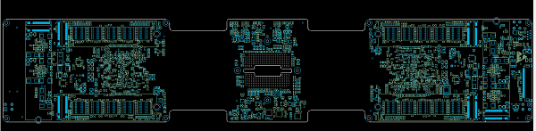
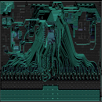
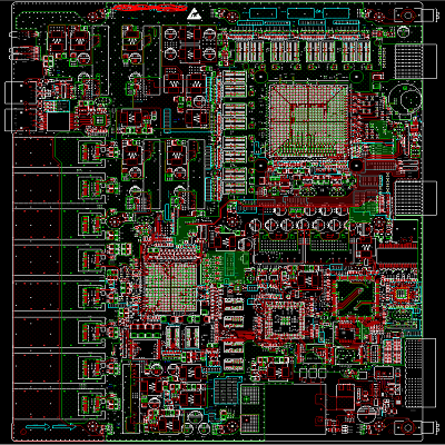
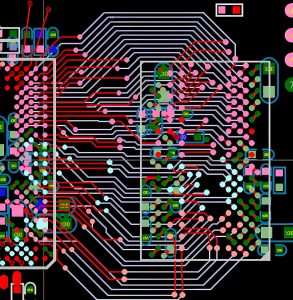
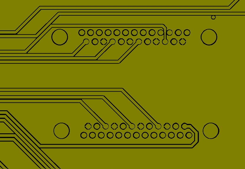
When designing high-speed PCBs, several critical factors must be considered to ensure optimal performance. These include signal integrity, impedance control, and minimizing electromagnetic interference (EMI). Below is an ultra high speed camera PCB solution made by Best Technology:
An ultra-high-speed camera rigid-flex circuit board
[1]: XCKU060 chip
[2]: 20A maximum current
[3]: Four DDR4 channels
[4]: 20 layers PCB
Camera PCB design considerations:
1. When the Camera adopts a connector: when the MIPI differential signal passes through the connector, the adjacent differential signal pairs must be isolated using GND pins; If it is not convenient to punch holes, the spacing between the difference pairs is at least 15mil.
2. If there is a reserved test point for the Camera connection seat, it should be close to the connection seat, and the Stub on the cable should be as short as possible.
3. Decoupling capacitors of AVDD/DOVDD/DVDD power supply need to be placed as close as possible to the Camera connection base.
4. The Camera layout needs to be far away from high-power radiation devices, such as GSM antennas.
5. CIF/MIPI and other signals, if there is a board to board connection through the connector, it is recommended that all signals be connected with a certain resistance value (between 2.2ohm and 10ohm, depending on the SI test), and reserve TVS devices.
Best Technology offers one-stop solutions for our values customers. And we provide free technical support for our customers. If you have similiar requirements, welcome to contact us at any time!
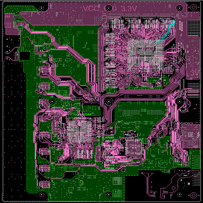
PCB design is one of an important process before the PCB manufacturing, it determines the overall performance of the whole product. We are an experienced PCB design and manufacturing vendor, with our professional technical team and advanced evaluated tools, we can make sure the PCB design one-time success. Today, we shared a example of fiber optical SFP modules design:
32X100G(QSFP28) large capacity convergence shunt
[1]: Marvell: 98CX8522
[2]: Single pair differential line, 25G optical network
[3]: 16 layers PCB
How to design a SFP optical module PCB?
SFP optical module interface PCB design depends on many aspects, including interface signal processing, timing control, power management and so on.
1. Determine the interface standard: SFP optical module interface standards, such as SFP, SFP+, QSFP and so on, you need to choose the appropriate interface standard according to the specific needs.
2. Choose the chip solution: According to the interface standard, choose the appropriate chip solution, usually including constant voltage source, amplifier, comparator, clock generator, EEPROM, etc.
3. Signal processing: For receiving and sending signals, filtering, amplification and comparison are required to ensure signal quality and stability.
4. Timing control: The timing and frequency of the clock signal need to be accurately controlled to ensure the correctness and stability of data transmission.
5. Power management: SFP optical module interface requires multiple power supplies, including Vcc, VCC-TX, VCC-RX, etc. Reasonable power management is required to ensure the stability and reliability of the power supply.
6. PCB design: According to the above requirements, PCB design is carried out, considering signal isolation, layering layout, status separation, signal integrity and other factors.
Feel freely to send message us if you are interested in PCB design.
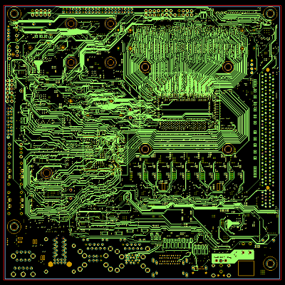
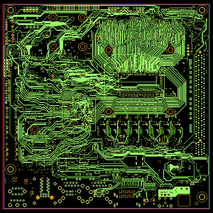
A motherboard network adapter PCB comprises several key components, each playing a vital role in ensuring effective network connectivity. And between them, the PCB is the most important. Now, best technology is sharing an example about motherboard network PCB design.
10G/100G large capacity convergence shunt
[1]: Marvell: 98DX8548
[2]: 21A maximum current
[3]: Single pair differential line, 10G and 25G optical networks
[4]: 10 layers PCB
What are the considerations before PCB design?
PCB design involves several steps and some considerations need to be noticed. If you are a designer, think about these points before starting the design.
Manufacturing: prototyping study or mass production.
What it will be used in?
What kind of production technology it will used?
Material?
How many layers you want?
Whether need to do impedance control?
Best Technology has more than 17 years in this industry, we have served for over 1200 customer all around the world. Our goal is to provide customer with best solutions and top notch quality products, and it is luckily that we did a good job. If you want to work with us or need a PCB manufacturer in Asia, contact us right now!
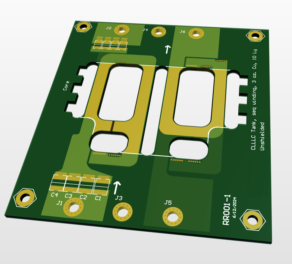
A high-speed circuit handles signals that switch quickly or operate at high frequencies, typically above 50 MHz, though some advanced systems may go into the GHz range. Best Technology is a one-stop PCB manufacturer that covers pcb design, pcb layout, pcb diagram, DFM, SI, PI analysis, PCB manufacturing and so on. In the following, you can see a high speed pcb design solution for industrial switch that we cooperated with our customer.
32 x 400GE industrial switch
[1]: Marvell-400G chip
[2]: 200A maximum current
[3]: Single pair differential line 56G optical network
[4]: 24 layers high power PCB
What’s the Best Material for High-Speed PCB Design?
Choosing the right material is vital for maintaining signal integrity and achieving optimal performance. The material impacts the board’s dielectric constant (Dk), loss tangent, and overall signal quality. Common materials include:
FR4: Widely used but not ideal for very high frequencies due to higher loss tangent.
Rogers (RO4000 series): Preferred for high-speed designs thanks to its low dielectric constant and loss tangent.
Teflon: Excellent for high-frequency applications but more expensive and harder to process.
Selecting the appropriate material ensures the PCB can handle high-speed signals without compromising performance.
For the PCB design service, we can make sure the one-time success to save much time and money for customers. Our goal is to work with customers together and win more market with our clients. Just feel free to contact our technical team if you have similiar designs.
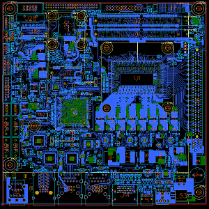
Best technology offers numerous PCB design solutions for our customer, from HDI design, high speed device PCB design, AI optical module design and network motherboard design for network switching. Below is one of our network motherboard design solutions:
An ATCA network switching motherboard
[1]:BCM88XXX, BCM55XXX chips
[2]:60A maximum current
[3]:8口10G optical network
[4]: 8 x DDR3 chips
Network Switching Differential Pair Design Guide
Each TrxP/TrxN signal group (where xcx0-3) shall be routed as a differential pair. This includes the entire length of wiring processing.
The individual differential correspondences are packed together as tightly as possible. Impedance calculations are usually started by selecting the smallest line blank (4-5mil). The tracking width is then adjusted to achieve the necessary impedance.
Differential line group resistance of Ethernet is calculated at 100 ohms.
In general, when routing the four differential pairs of the Gigabit Ethernet to the r45 connector, at least one pair will pass through to the opposite outer layer.
Priority should be given to differential pair wiring. Terminals should be added after the routing is determined
The values of all resistance terminals in the Ethernet front end should be 1.0% tolerance
All capacitor termination Ethernet front ends in the module should have strict tolerances and high quality product media (npo)
You are welcome to contact us if you want to get your DIY network switching PCB designs.
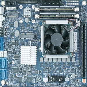
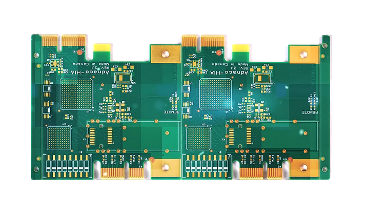
Best technology engaging in the PCB manufacturing and PCB design for more than 17 years. With a strong R&D team, we can provide customers with fast and valued PCB design solutions. Here is one of our industrial motherboard design & industrial PCB case sharing for your reference. If you want to get your own industrial PCB design, welcome to contact us.
A mITX architecture industrial control motherboard
[5]:2x USB 3.0 (Internal) + 1x USB 3.0 (Client) + 2x USB 3.0 (Rear I/O) + 2x USB 2.0 (Rear I/O) +
2x USB 2.0 (Front Header) + 1x USB 2.0 (mPCIe)
Industrial PCB Design Considerations
Control the length of the circuit: Minimize the length of the circuit, especially the key signal lines, to reduce signal attenuation and delay.
Avoid sharp angles and right angles: Right angles and sharp angles should be avoided when wiring, and rounded or 45 degree angles should be used as far as possible to reduce signal reflection and impedance discontinuity.
Line width: Determine the line width according to the current size and thermal requirements to ensure the reliability and stability of the circuit.
Inter-layer wiring: Rational use of multi-layer PCB inter-layer wiring, such as the signal line on the inner layer, power and ground wire on the outer layer.
Impedance control: For high-speed signals, it is necessary to control the line impedance to ensure signal integrity, and carry out impedance matching design if necessary.
Avoid cross and parallel wiring: Try to avoid cross and parallel wiring of signal lines to reduce crosstalk and electromagnetic interference.
Contact us if you have any questions and inquiry about industrial PCB design projects.
PCB design not only including the routing layout, component placement also is a key parameter. It involves understanding electrical parameters, signal integrity, and thermal management. This article will introduce several golden rules of how to optimize your component placement, whether you are a novice or a seasoned professional, it is helpful for you to manage your circuit board design greatly.
Determine the power supply and grounding plane
In the early stage of PCB design, reasonable power supply and grounding layout is the key. The power supply and ground plane not only provide a stable power supply for the components, but also play a role in reducing electromagnetic interference (EMI). To begin the layout, the first thing is confirming the location of the power supply and ground area. Usually, the power is placed in a complete layer of the PCB, and the ground is in another layer, which can effectively reduce the power supply noise.
Make sure the power plane is close to the area where high power is needed, which can reduce the voltage drops along the supply path. The ground area should be as large and continuous as possible, this helps to provide a good return path and reduce interference from high-frequency signals.
Differentiate layouts by function
When laying out components, dividing the circuit board into different functional areas can improve the efficiency and performance of the design. For example, you can separate power supply into signal processing area, power management area, and interface. This method helps to reduce the mutual interference between different circuits and improve the overall stability of the circuit.
Please noted that, high-frequency components should be close to connectors or key interfaces to shorten the signal path and reduce interference. Low-frequency components can be placed away from critical signal paths to optimize overall signal integrity.
Keep short and direct trace
Shortening the length of signal lines is another important thing to optimize component layout. Make sure keep them short and direct as possible. Long distance signal routing may lead to signal attenuation and delay, which will affect the overall performance of the circuit. Placing the relevant components as close as possible. This not only reduces the length of the circuits, but also reduces the coupling and interference between the signals.
In addition, in the routing process, try to avoid right-angle (90 degrees) turns. Because the right angle will cause signal reflection, affecting the integrity of the signal. Try to use 45 degree turns or arc turns to reduce signal loss.
Consider heat dissipation requirements
Heat management is an important consideration when placing high-power components. Place power components in the edge area of the PCB, such as power transistors and high-frequency converters. This facilitates the use of natural air flow for heat dissipation and convenient for the installation of external cooling devices.
In high-density designs, through-holes, vias and cooling copper blocks can be designed on the PCB, which can transfer heat to the inner layer or bottom of the PCB to help dissipate heat. In addition, maintain a reasonable distance between each component to promote air flow and heat dissipation.
Optimize test points position
Consider placing test points in a convenient location for testing and debugging. Placing test points close to relevant components simplifies the debugging process and reduces test complexity. In particular, the placement of test points on the key signal path can facilitate the detection and verification of signal integrity and stability in the design stage.
For example, the discrete components required for OpAmp operational amplifiers can be placed close to the device, so that the bypass capacitors and resistors can work with them. This helps to optimize the wiring length mentioned as above, while also making testing and fault detection easier.
Consider DFM & DFA factors
Optimizing component layout takes into account not only electrical performance, but also the actual requirements of manufacturing and assembly. For example, try to avoid placing components on both sides of the PCB to simplify the PCBA assembly process. The components are arranged neatly and spaced consistently, which helps the automated assembly equipment to operate efficiently and reduce assembly errors.
Properly using DFM (Design for Manufacturability) principles make production easier and more cost-effective. Ensure that your design can be fabricated with standard processes.
Perform DRC as often as possible
Although it only takes a short time to run DRC (Design Rule Check) functionality on PCB software. But in some complex design environments, perform checks during the design process can save a lot of time, which is a good habit to keep. Every layout routing decision is critical, and running DRC can remind you of the most important layout at any time.
Check production files before sending to manufacturer
While most of PCB manufacturers are happy to download it directly and verify it for you, it is best to export the Gerber file yourself and use the free software such as Gerberv to check that it is as expected to avoid misunderstandings. By verifying it yourself, you may even find some inadvertent errors and thus avoid the cost of completing the production according to the wrong parameters.
Successful PCB design cases – Best Technology
A: A mITX architecture industrial control main board
[5]:2x USB 3.0 (Internal) + 1x USB 3.0 (Client) + 2x USB 3.0 (Rear I/O) + 2x USB 2.0 (Rear I/O) +
2x USB 2.0 (Front Header) + 1x USB 2.0 (mPCIe)
Anyway, communicating with your manufacturer to understand their equipment and processes can optimize the design, reduce manufacturing problems, improve production efficiency and product quality.
Although semiconductor integration is increasing, many applications have ready-to-use systems on chip. And there are various powerful and out-of-the-box development boards are becoming more readily available, many use cases in electronics still require the use of custom PCBs. In one-time development, even an ordinary PCB can play a very important role. This article will introduce several golden rules of PCB design, and are widely applicable to various PCB design projects.
What are the golden rules of PCB design?
The golden rules of PCB design serve as the foundation for a robust layout. Remember below top 5 rules can help you in PCB designing.
Optimize component placement
Select correct crosstalk
Make sure short and straight circuits
Manage the distribution of power and ground circuit whenever possible.
Avoid sharp angles in traces, opting for 45-degree turns instead.
Additionally, always perform Design Rule Checks (DRC) to catch potential issues before finalizing the layout. These checks help ensure compliance with manufacturing and performance standards.
What are the top 3 important steps in PCB design and layout process?
The PCB design and layout process has many important steps, but these three processes should be given priority.
1. Schematic design and component selection
Start by creating a detailed schematic diagram of your circuit board. As a designer, you can choose discrete components with high or low component values, but with the same performance. By consolidating within a smaller range of standard values, the bill of materials (BOM) can be simplified and potentially cost reduced.
Select suitable components based on the requirements of your design, considering factors like voltage, current, and signal frequency. A clear and precise schematic is essential. It helps avoid errors and streamlines the layout process, making it easier to place and route components effectively.
2. Component placement
Arrange components strategically on the board. Place critical components like microcontrollers and high-frequency ICs first, followed by supporting components. Consider heat dissipation and accessibility for debugging. If you have a range of PCB products based on preferred component values, it will also help you make the right inventory management decisions in the longer term.
3. Routing
Routing including connecting the components with traces. Prioritize routing for critical signals first, such as clock lines and high-speed data paths. Use the shortest possible paths and avoid crossing different signal types to reduce interference. After critical traces, route the power and ground nets, followed by less critical signals. Utilize multiple layers if needed to keep the layout clean and manageable.
What are the guidelines for PCB layout?
PCB layout guidelines can help designers achieve optimal component placement and ensure the board is easy to assemble. Here are some things to consider:
1. Trace width and spacing
Maintain appropriate trace width and spacing based on current carrying capacity and voltage levels. The IPC-2221A standard provides recommendations on PCB trace width and spacing. According to this standard, the trace width must be selected based on current-carrying capacity and permissible temperature rise. For instance, a 1mm wide trace with 1oz. copper (35μm) can carry approximately 2.5A with a 10°C temperature rise.
2. Layer stack-up
Design your PCB stack-up carefully. Multilayer designs are typically used in high-frequency applications to effectively separate power, ground, and signal layers, thereby reducing electromagnetic interference (EMI). Studies show that in a 4-layer or more stack-up, closely coupling the power and ground planes can significantly reduce EMI and improve signal integrity.
3. Thermal management
Consider thermal aspects in your layout. Place components that generate significant heat, such as power transistors, away from heat-sensitive components. Use thermal vias and heat sinks to manage heat dissipation effectively.
4. Via placement
Use vias strategically to connect different layers. Avoid placing too many vias close to high-frequency signal paths to prevent signal degradation. Use via stitching to enhance ground planes and reduce loop areas.
5. Power distribution
Using wide traces for power and ground planes is critical to minimizing resistance and inductance. For instance, IPC-2152 provides guidelines on power distribution and suggests using wide traces to handle higher currents and minimize voltage drops.
What are the considerations of PCB layout?
When designing a printed circuit board, you can consider these points:
1. Signal integrity
Maintain signal integrity by minimizing trace lengths and avoiding impedance mismatches. Use differential pairs for high-speed signals and keep them close together to reduce noise.
2. EMI/EMC
EMI and EMC are critical considerations. Use proper shielding and grounding techniques to mitigate interference and ensure compliance with regulatory standards.
3. Design for Manufacturability (DFM)
Ensure your layout is manufacturable by adhering to fabrication capabilities and tolerances. Simplify routing and avoid excessive component density to facilitate easier assembly and inspection.
4. Mechanical constraints
Consider the physical dimensions and mounting requirements of your PCB. Ensure that components and traces do not interfere with mechanical parts or enclosures.
5. Cost
Optimize your design for cost by reducing layer count where possible and minimizing the use of expensive materials or processes. Balance performance requirements with budget constraints.
At Best Technology, we offer expert design services to help you achieve your project goals with precision and excellence. Choose us for your next PCB project and experience the benefits of quality and innovation.
In the design of electronic products, electromagnetic compatibility (EMC) is a crucial consideration. Particularly in the design of printed circuit boards (PCBs), the rationality of EMC design directly impacts the performance and stability of the product. Among the many factors affecting EMC, one factor is especially critical, and that is the design of the ground plane. Today, let’s talk about the impact of grounding on EMC.
In an electronic product, grounding is a very important element, it is directly related to EMC compliance. Especially in large equipment, the grounding of multiple systems and subsystems is involved. It can be said, a good grounding system means the half successfully of a product.
What are Ground Plane and EMC in a PCB?
The ground plane, as the reference potential in a circuit, not only carries the return path of current but also plays a role in electromagnetic shielding and noise suppression. In high-frequency circuits, the impedance and layout of the ground plane have a significant impact on signal integrity. Unreasonable ground plane design may result in signal interference, increased radiation, and decreased system stability.
EMC stands for Electromagnetic Compatibility. It refers to the ability of electronic devices and systems to operate properly in their intended electromagnetic environment without causing or experiencing interference. EMC ensures that devices can function without adversely affecting other devices nearby or being affected by electromagnetic interference from external sources. Generally, the ground planes will showing three shapes, please see as following:
Why A Grounding Must be Designed in PCB?
Grounding can be understood as an equipotential point or plane serving as the reference potential for a circuit or system, which can be a specific ground layer in a PCB or the metal chassis of a product. While many perceive the purpose of designing a ground plane primarily to prevent external electromagnetic interference (EMI), but in printed circuit board design, it serves multiple purposes beyond this.
Generally, a well-designed ground provides a common reference zero potential for all circuit units within a system, ensuring no potential difference between circuits and thus stable operation. It also protects circuits from damage, ensuring the safe functioning of electronic products. For instance, ground can provide discharge paths for transient disturbances and dissipate accumulated charges on product metal enclosures induced by static electricity, to prevent potential sparks that may cause interference internally. Additionally, choosing appropriate grounding for shielding structures can yield effective electromagnetic shielding.
Grounding design is very necessary especially for medical industry. As we know, there are many medical devices are directly connected to patients’ bodies, such as monitors. In cases where the chassis carries voltage due to poor grounding, fatal risks may arise. Furthermore, grounding reduces common-mode interference currents flowing through PCBs and prevents high-frequency EMI signals within products from reaching equivalent radiating antennas. Thus, grounding is typically a primary method for noise suppression and interference prevention.
Design Principles of Ground Plane in PCB
A well-designed grounding system should not only consider the radiation and conduction of individual PCBs but also prevent from a systemic perspective. In the design phase, failure to carefully consider the grounding system may indicate a high likelihood of EMC failure for the system. So, knowing the design principles is extremely important to make sure the successful of EMC.
Keep it short and wide
To reduce the impedance of circuits, especially in high-frequency circuits, the ground plane should be made as short and wide as possible. This helps to minimize the return path of the current, thereby reducing EMI.
Partition layout
For complex PCB designs like multilayer PCBs, it is recommended to use a partition layout to separate the ground planes of different functional modules. This helps to isolate noise interference between different modules.
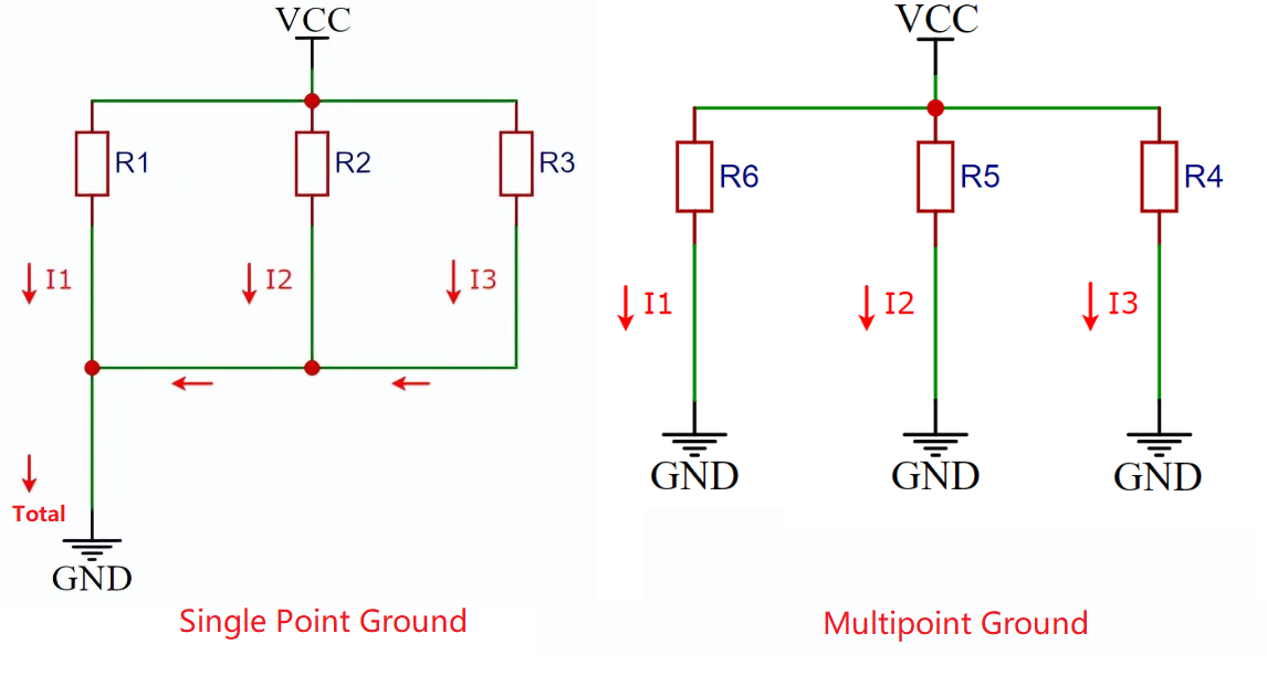
Single-point ground and multipoint ground
Depending on the circuit’s operating frequency and signal characteristics, choose between single-point grounding or multipoint grounding. Single-point grounding is suitable for low-frequency circuits, while multipoint grounding is more suitable for high-frequency circuits.
Ground plane
Where possible, use a ground plane as the ground. The ground plane can provide a low-impedance return path and aid in electromagnetic shielding.
How to Optimize Your Grounding Design?
As for PCB that has already design the circuit layout, how to optimize the ground to get the maximum EMI? Here are some tips that may helpful for you.
Fill the blank areas of the PCB with ground planes to increase the ground plane’s area and reduce impedance.
Reducing the area of ground loops helps to decrease electromagnetic radiation and induced noise.
Power lines and ground planes should be placed as close as possible and run parallel to reduce the area of the current loop.
Placing decoupling capacitors between power and ground planes helps to filter out high-frequency noise.
In PCB EMC design, ground plane design is an essential step that cannot be ignored. By following the principles and optimization methods of ground plane design, the EMC and signal integrity of electronic products can be significantly improved. Therefore, in PCB design, sufficient attention and consideration must be given to ground plane design. Welcome to contact Best Technology if you want to know more about ground and EMC design.
Electronics devices and parts are existing everywhere in this big data era, and more and more engineers trying to step in the electronics design and development. As a one-stop PCB and PCBA manufacturer in China, Best Technology would like to share some basic considerations and tips during the PCB designs. Hope this can help you.
Substrate Material
Substrate is the main composition of a circuit board and it mainly used for suppler and copper foil insulation. The commonly materials are FR4 and PI. FR4 is a widely acceptable international grade for fiberglass reinforced epoxy laminated, and it always used for making rigid PCB or rigid-flex PCB. FR4 substrate has good insulation and mechanical strength, so it can be widely used in various applications. However, PI has higher heat and chemistry resistance, more suitable for high temperature and chemical corrosion environment.
Circuit Layout
The layout design depends on the dimensions, performance and reliability of a circuit board, it is needed to follow your supplier’s standard to make sure the fast production time and high quality.
Min line width
Please make sure your line width within your supplier’s manufacturing capability, that is to say, if it is less than the minimum line width will not able to be produced. The best way is if the design conditions available, the larger the line width, the better the factory production. Generally, the line width keeps around 10mil is the best. In another word, if your line width is less than normal standard, it would be difficult for you to find a suitable supplier.
Min line spacing
Min line spacing means the distance between trace and trace. Normally, from the production aspect, the distance from line to pads should not less than min line spacing, and it would be better if it is larger, generally equal to or more than 10mil.
The spacing between circuit to outline should be control in 20mil.
Plug-in Hole
The diameter of plug-in hole should be considered by the side of components, but it is necessary that it must greater than the component’s pins, it is recommended that greater at least 0.2mm. That is to say, if the pin of components is 0.6mm, then the plug-in holes should be greater than 0.8mm. Otherwise, the plug-in components would be probably difficult to insert into PCB because of the tolerance control during the manufacturing and assembly.
Min Hole Diameter
As we all know, the holes in PCB almost be used for mounting components, connect circuit and provide the electrical connection between layers. So how to design the hole also is crucial during the designing. Generally, the min hole diameter depends on the drill bitter that vendor used, always around 0.2-0.4mm. You can ask your supplier during the design evaluation.
Copper Thickness
Copper foil is a layer of metal foil on the PCB board that is used to conduct current. The thickness of copper foil is usually in oz (ounces), such as 1oz, 2oz, 3oz, etc. The thickness of the copper foil will affect the conductivity and heat dissipation performance of the PCB board.
Impendence Control
Impedance control is a key parameter in high-speed signal transmission and high-frequency circuit design. It involves board thickness, copper foil thickness, substrate dielectric constant, pad and line layout and other factors to improve the signal integrity and anti-interference ability of the PCB board.
The production process of PCBs is rather complex, involving a wide range of techniques from simple mechanical processing to sophisticated machining, so you should understand the design rules very clearly when you are trying to design a PCB board. Its applications are also diverse, from consumer electronics to industrial machinery, where PCBs are utilized.
Best Technology offers one-stop PCB solutions, we offer service from prototyping to large-scale production and assembly. With experienced engineers and service teams, we ensure successful fulfillment of your requirements. Just send us with your design files, and we will make the circuit board for you in a very short time.