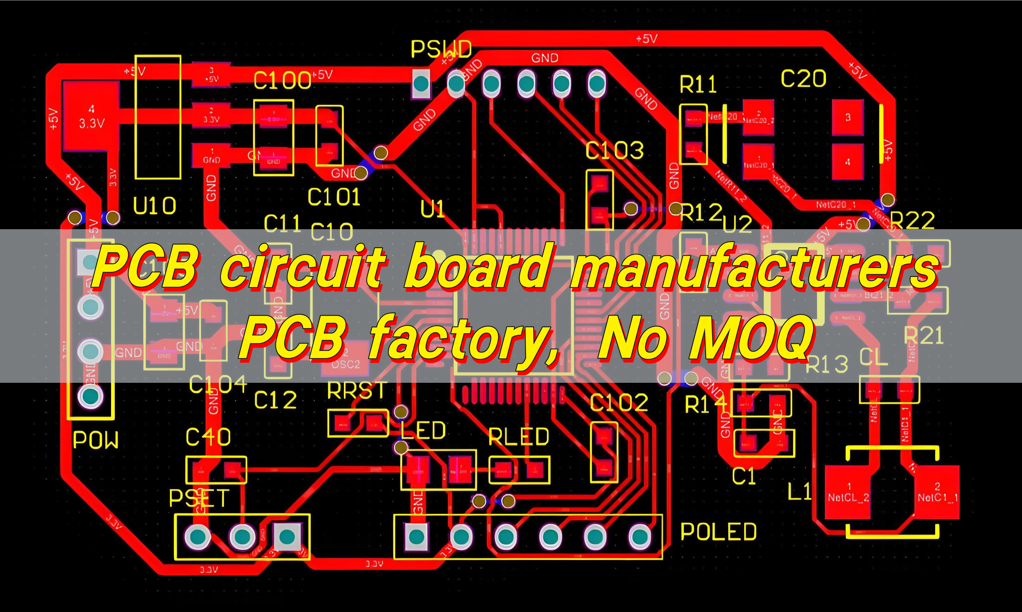
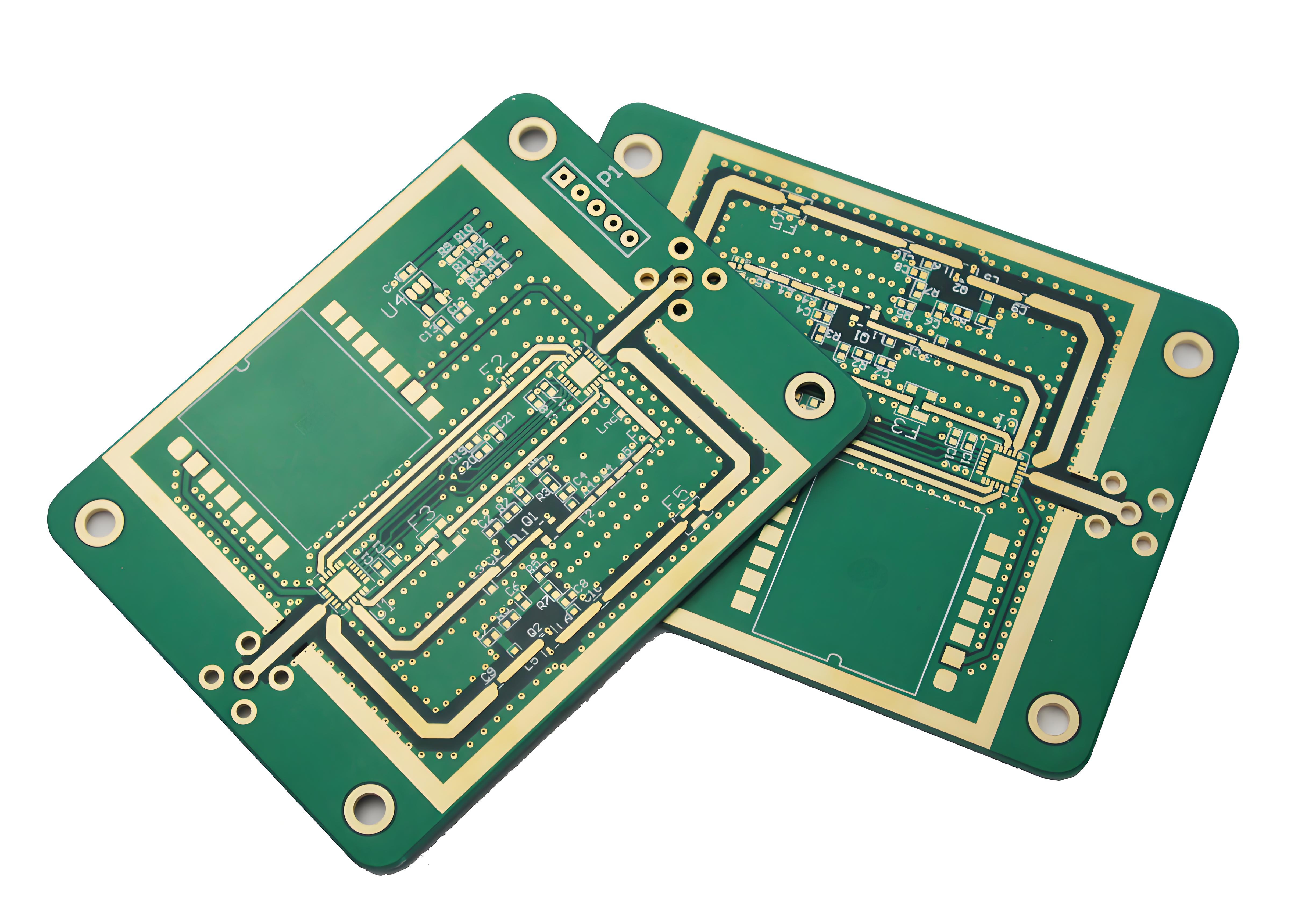
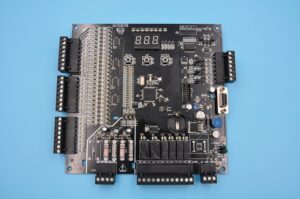
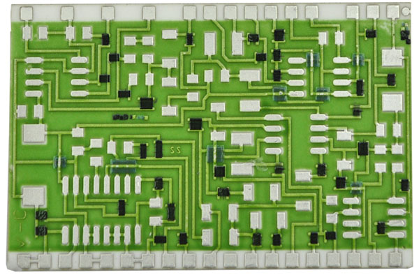
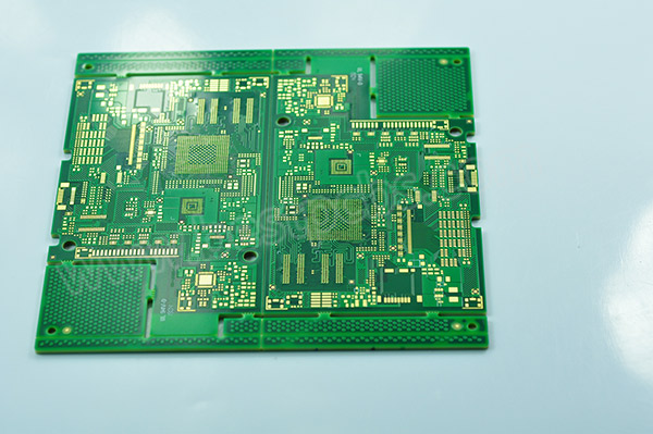
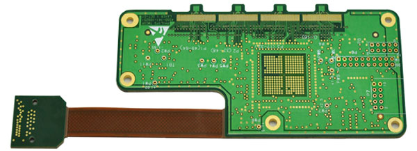
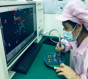
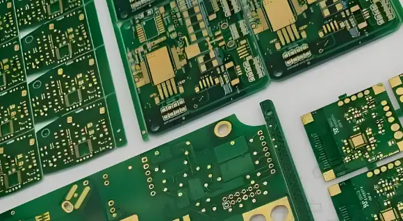
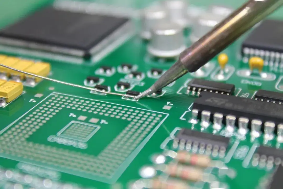
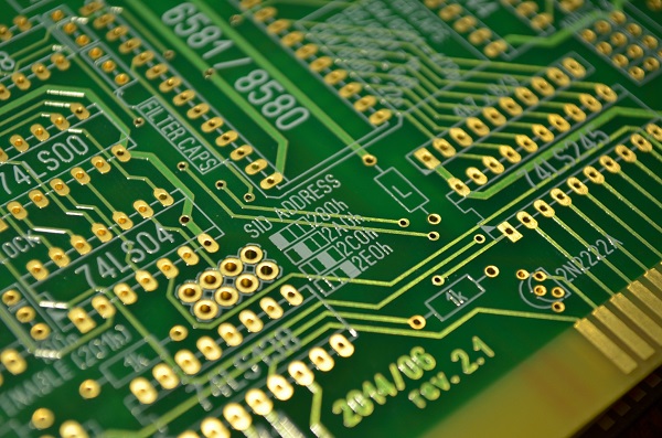
As a PCB Circuit Board Manufacturers, EBest Circuit (Best Technology) is committed to becoming your partner for high-precision PCBs, providing various types of circuit boards.
Are you looking for reliable PCB circuit board manufacturers? Do you have the following questions?
- What industry certifications does your factory have?
- How many layers of circuit boards can you produce?
- What types of PCBs do you specialize in?
- How do you ensure PCB quality?
EBest Circuit (Best Technology) is your best choice and can solve your concerns~
- We are ISO 9001, IATF 16949, and UL certified. We strictly adhere to IPC standards for production and inspection, ensuring our quality system meets international standards.
- We can consistently produce multi-layer boards with 1-32 layers, with a minimum line/space accuracy of 2/2 mil (50μm) in mass production, meeting most high-precision design requirements.
- We specialize in high-reliability PCB manufacturing, with extensive experience and technical advantages in high-frequency, high-speed boards, HDI boards, rigid-flex boards, and metal substrates (heat-dissipating aluminum substrates).
- We utilize comprehensive inspection equipment such as AOI (Automated Optical Inspection), flying probe testing, and X-ray inspection, combined with strict process control (IPQC/IQC) to ensure the quality and reliability of every PCB.
If you have any PCB needs, please contact us: sales@bestpcbs.com
How to design a PCB circuit board?
BEST Technology engineers first define the board’s functionality, power requirements, and size. A simple prototype or schematic follows. Good planning avoids costly rework later.
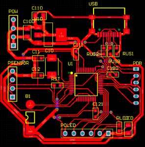
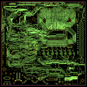
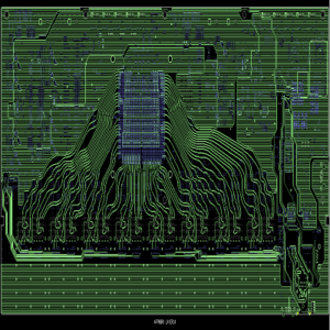
Next, designers use electronic design automation software such as Altium or KiCad. These tools map every trace, pad, and via. Each copper path must handle the right current while avoiding interference. Shorter paths mean less signal loss.
High-speed signals should travel straight and short. Sensitive parts like sensors stay away from noisy circuits.
After layout, we create Gerber files. Gerber files show each layer, drill hole, and mask. A quick design review catches errors before fabrication.
Collaboration with experienced circuit board manufacturing companies helps here. BEST Technology engineers will provide more optimal cabling or stacking solutions. This feedback can save time and reduce risks.
How to make PCB circuit board?
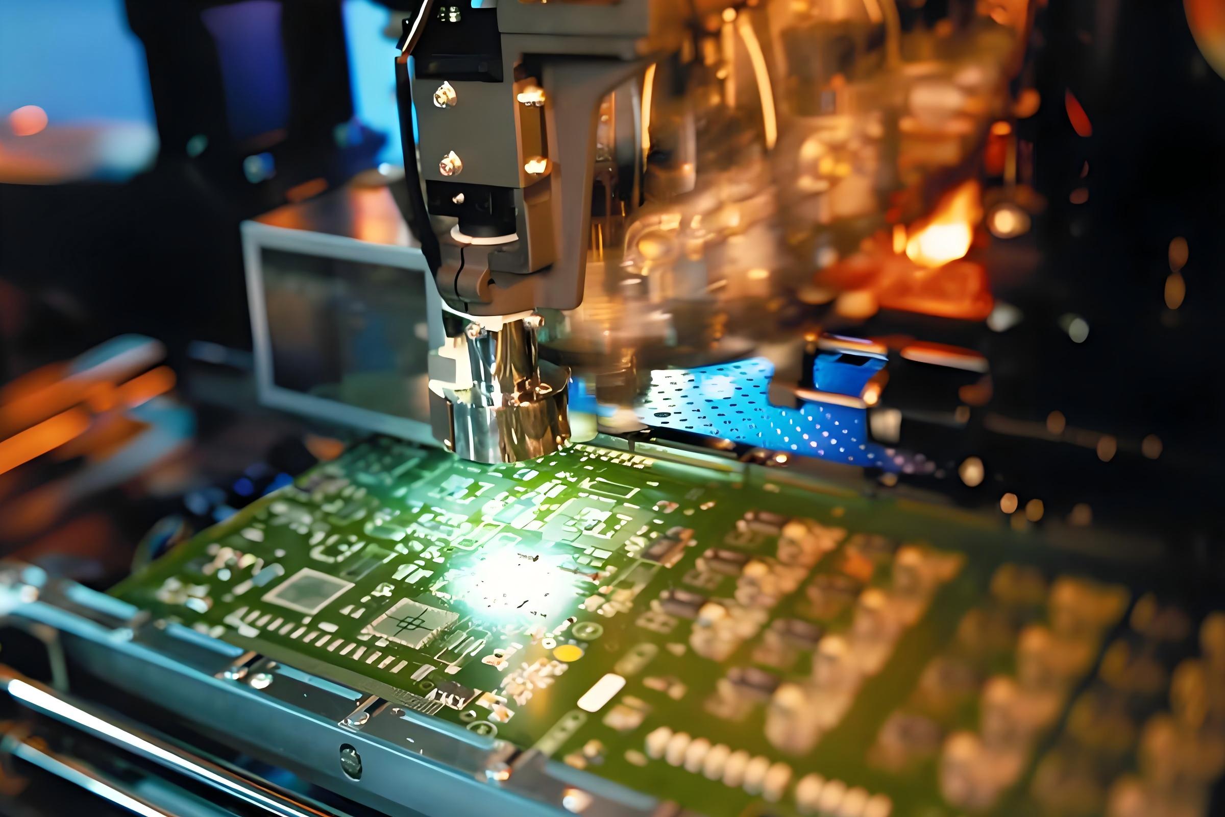
Once design files pass review, production begins. First comes imaging. The factory prints the circuit pattern onto copper-clad laminate using a photoresist film. Light hardens the image, and unwanted copper is etched away. The result is a clean network of copper traces.
Drilling follows. Precision machines create micro-holes for vias and through-hole parts. Laser drilling handles very small features common in today’s compact devices.
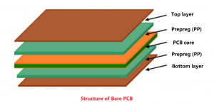
Plating adds a thin copper layer inside holes, creating reliable connections between layers. For multi-layer boards, technicians press and heat inner cores together, bonding them with resin.
Next is solder mask. This green (or sometimes blue, red, or black) coating protects copper and keeps solder only where needed. Silk-screening then prints component labels and logos.
Electrical testing is critical. Automated probes check continuity and isolation. Any shorts or open circuits trigger rework.
Finally, the panel is cut into individual boards. Each product is cleaned, packaged, and ready to be shipped to the assembly line or directly to you.
Which PCB manufacturing steps matter most?
Every step counts, but three stand out.
- Imaging and Etching: Accurate imaging ensures the circuit matches design specs.
- Drilling and Plating: Proper plating guarantees strong inter-layer connections.
- Testing: Rigorous electrical tests catch defects before assembly.
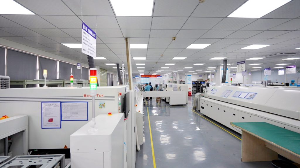
BEST Technology uses advanced equipment and strict quality controls during these critical stages. Automated optical inspection, clean rooms, and real-time monitoring protect consistency.
What is in a circuit board components list?
A circuit board components list, often called a bill of materials (BOM), details everything needed for assembly. It includes:
- Integrated Circuits (ICs): Microcontrollers, processors, memory chips.
- Passive Components: Resistors, capacitors, and inductors that manage current and voltage.
- Connectors: USB, HDMI, headers, and terminals to link with the outside world.
- Discrete Semiconductors: Diodes, transistors, MOSFETs.
- Special Parts: Sensors, antennas, or displays unique to your design.
Each item specifies part numbers, tolerances, and approved suppliers. A clean BOM speeds sourcing and lowers cost.
BEST Technology, as an experienced printed circuit board PCB manufacturers, usually helps to complete the list and recommend parts with a stable supply and better prices.
Which materials do PCB factories use?
The foundation of a PCB is the laminate. FR-4, a fiberglass-epoxy composite, remains the industry standard. It balances strength, thermal resistance, and cost.
For high-frequency or high-speed boards, BEST Technology’s factories will use materials such as Rogers or polyimide. These offer lower dielectric loss and better heat performance.
Copper foil forms the conductive layers. Thickness ranges from 0.5 oz to 3 oz per square foot depending on current needs.
Solder mask is usually epoxy-based for durability. Surface finishes like ENIG (Electroless Nickel Immersion Gold), HASL (Hot Air Solder Leveling), or OSP (Organic Solderability Preservative) protect pads from oxidation and improve soldering.
What drives PCB manufacturing cost and speed?
Several factors influence cost and lead time.
- Layer Count: More layers mean more drilling, lamination, and testing.
- Board Size and Quantity: Larger or thicker boards use more material and require longer machine time.
- Trace Width and Spacing: Fine pitch designs demand tighter process control and raise cost.
- Surface Finish: Gold plating and advanced coatings cost more than simple HASL.
- Testing Level: Flying-probe or functional tests add time but ensure reliability.
To speed up production, BEST Technology, a top PCB manufacturer, uses automated production lines and intelligent scheduling. We also offer a no-minimum-order option, allowing for rapid prototyping without waiting for volume orders.
What certifications should circuit board manufacturing companies hold?
Quality certifications prove a factory follows global standards.
- ISO 9001: Shows strong quality management across the entire process.
- UL Certification: Ensures boards meet safety standards for flammability.
- RoHS and REACH Compliance: Confirms materials are free of restricted hazardous substances.
- IATF 16949: Important for automotive electronics.
- ISO 13485: Required for medical device PCBs.
Working with certified circuit board manufacturers protects your product and brand reputation. We hold relevant quality certifications that validated our commitment to provide high quality products. These certificationsact as a guarantee of product excellence, ensuring customers and partners a good quality assurance practices.
How to pick the best PCB circuit board manufacturer?
Selecting the right partner means balancing technology, service, and flexibility.
Start with capability. Does the factory handle your board size, layer count, and finish? Do they support rigid-flex or HDI if you need them?
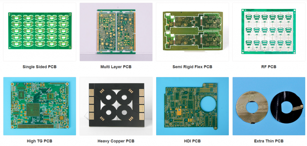
- BEST Technology begin to As a printed circuit board (PCB) vendor in Asia, we are dedicated to be your best partner of advance, high-precision printed circuit boards, such as heavy copper boards, mixed layers, high TG, HDI, high frequency (Rogers, Taconic), impedance controlled board, Metal Core PCB (MCPCB) such as Aluminum PCB, Copper PCB, and so on.
Established PCB manufacturer teams know how to solve complex issues and scale from prototype to mass production.
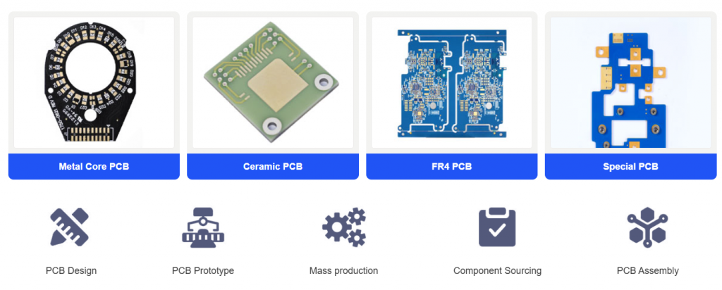
- EBest Circuit (Best Technology) provides rapid PCB prototyping services. We provide PCB prototype service with FR4 PCB, Ceramic PCB, MCPCB, HDI PCB, heavy copper PCB, High TG PCB, RF PCB and so on. Pls let us know if you have any questions about PCB.
Look for transparent communication. A reliable supplier provides clear quotes, fast technical feedback, and regular updates.
- EBest Circuit (Best Technology) provides full turnkey services in China with more than 19 years of experience, We’ll respond to your inquiries 24 hours a day, providing the best services at competitive prices.
Evaluate speed and flexibility. A factory offering no MOQ lets you order small runs for testing without penalty.
- Best technology No MOQ quantity requirement, even 1 piece, we can help you.
Finally, consider support. Post-delivery service and warranty show confidence in their product.
- Based on our strict quality control system, we are so confident in our product that will guarantee money-back for any defective products. We will re-fabricate the boards for free or make refund with no reason. You don’t need to worry anything!
EBest Circuit (Best Technology)’s one-stop service—from design input to assembly—can help you quickly move from idea to market.
When you seek dependable PCB circuit board manufacturers or a PCB factory with no MOQ, choose a partner with proven experience and strong service. BEST Technology ensures your project starts on time and runs smoothly.
For inquiries or custom quotes, please email sales@bestpcbs.com


