pcb
Home > Blog

Posts Tagged ‘PCB’

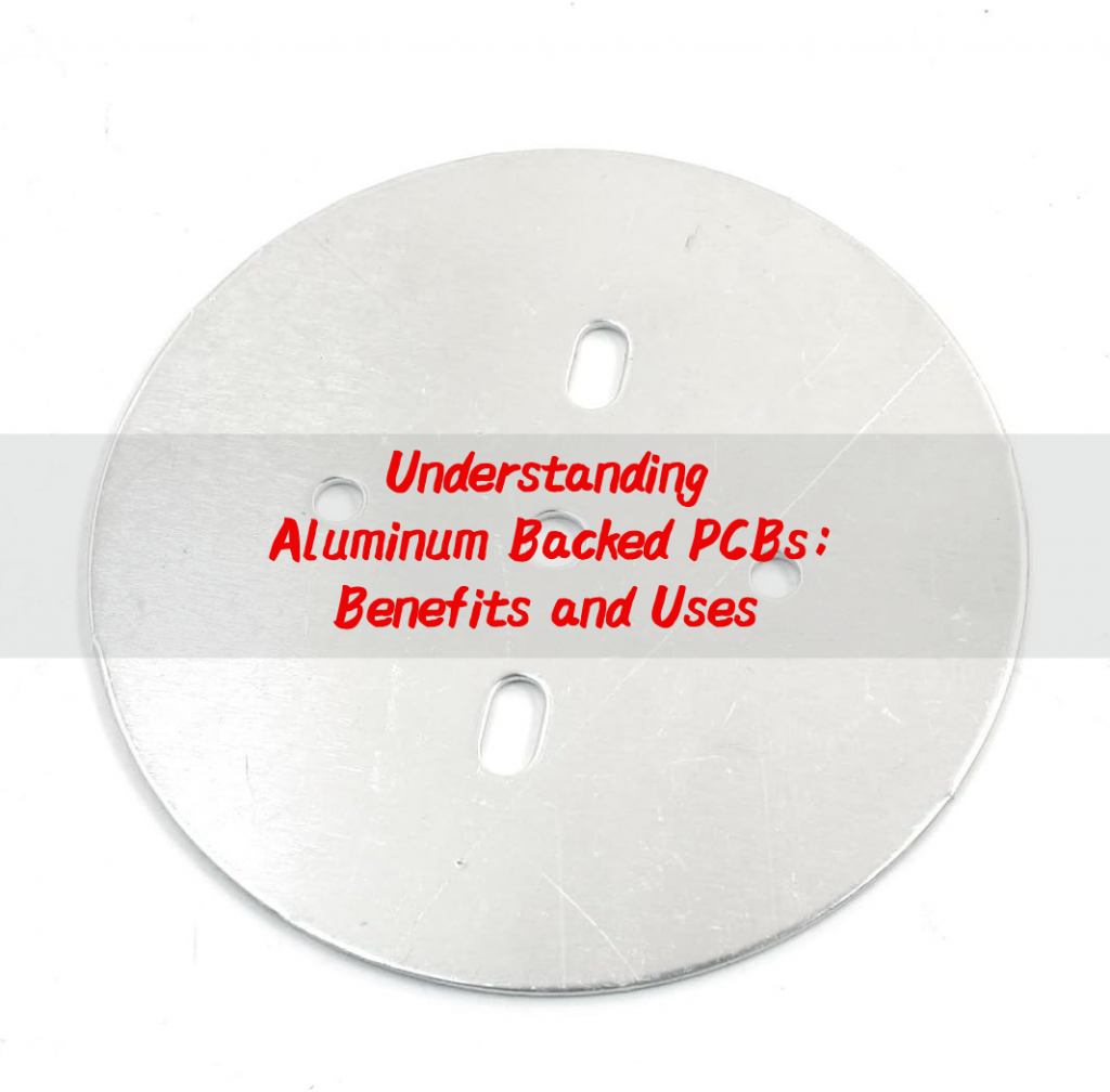
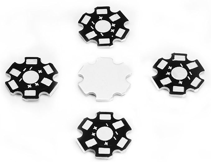
What is aluminum base pcb board? How to choose?
Wednesday, September 25th, 2024

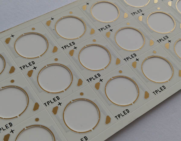
As a new type of PCB material, aluminum base pcb board is gradually becoming a popular choice in the electronics field with its excellent performance and wide application fields.

What is aluminum base material PCB?

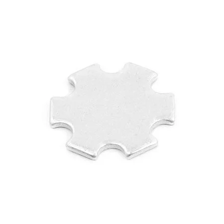
Aluminum base material PCB (Printed Circuit Board) refers to a special type of PCB that uses aluminum as the substrate material. This PCB usually includes three main parts:

What is aluminum base pcb board? How to choose?
  • 1. Circuit layer: This is the part where the circuit pattern is installed, usually a layer of copper foil, which is etched to form a circuit path.
  • 2. Insulating thermal conductive layer: Located between the circuit layer and the metal base layer, this layer of material not only needs to provide electrical insulation between circuits, but also has good thermal conductivity to transfer the heat generated when the circuit is working to the metal base layer.
  • 3. Metal base layer: Usually a layer of aluminum plate, its function is to quickly dissipate the heat from the circuit layer.

Due to its good thermal conductivity, aluminum base PCB is very popular in application scenarios that require efficient heat dissipation, in LED lighting, power management, automotive electronics, communication equipment, and other electronic devices that require high power output and good thermal management.

Compared with traditional FR-4 fiberglass PCBs, aluminum base pcb boards can manage heat more effectively, thereby improving the reliability and life of electronic components. ‌

Why Aluminum is used in PCB?

There are several main reasons for using aluminum in PCBs (printed circuit boards):

1. Good heat dissipation performance

  • High thermal conductivity: Aluminum is an excellent thermal conductive material with a relatively high thermal conductivity. During the operation of the PCB, electronic components will generate heat, and the aluminum substrate can quickly conduct this heat away to avoid damage to electronic components caused by excessive local temperatures, thereby improving the stability and reliability of electronic equipment and extending the service life of components.
  • Uniform heat dissipation: The aluminum substrate can evenly distribute heat across the entire PCB, prevent hot spots from concentrating, and reduce the risk of failures caused by local overheating.

2. Higher mechanical strength

  • Vibration resistance: Aluminum has a certain rigidity and toughness, and can withstand the vibration and impact that electronic equipment may be subjected to during use, which can ensure that the PCB will not be easily damaged by external forces.
  • Dimensional stability: The dimensional changes of aluminum substrates are relatively small under different temperature and humidity conditions, which can maintain the structural stability of PCBs and ensure the welding reliability of electronic components.

3. Good insulation performance

  • The surface of the specially treated aluminum substrate has a good insulation layer, which can effectively prevent circuit short circuits and leakage. At the same time, the insulation layer can also withstand a certain voltage to meet the electrical insulation requirements of different electronic equipment.
  • Good compatibility with other insulating materials: It can be well combined with the packaging materials and welding materials of various electronic components to ensure the overall performance of electronic equipment.

4. Good processing performance

  • Strong processability: Aluminum substrates can be made using traditional PCB processing techniques, such as etching, drilling, cutting, etc., which is convenient and fast and can meet different design requirements.
  • Surface processability: The surface of the aluminum substrate can be processed in a variety of ways, such as copper plating, gold plating, tin spraying, etc., to improve welding performance and corrosion resistance.

5. Cost-effectiveness

  • Relatively low material cost: Aluminum is a common metal material with abundant resources and relatively stable prices. Compared with some high-performance heat dissipation materials, the cost of aluminum substrates is low, which can reduce the manufacturing cost of electronic equipment while ensuring performance.
  • High production efficiency: Due to the good processing performance of aluminum substrates, large-scale automated production can be achieved, which can improve production efficiency and further reduce costs.

How to choose aluminum base pcb board?

Choosing the right aluminum base pcb board is crucial to the performance and reliability of electronic equipment. In the selection process, multiple factors need to be considered, including glass transition temperature, heat resistance, flatness, thermal expansion coefficient and electrical performance.

(I) Glass transition temperature

Glass transition temperature (Tg) is one of the important parameters for measuring the heat resistance of PCB substrates. Generally speaking, substrates with higher Tg are more stable in high temperature environments and are not prone to deformation or damage.

What is aluminum base pcb board? How to choose?

For application scenarios with higher operating temperatures, aluminum base pcb boards with Tg higher than the circuit operating temperature should be selected. The Tg of the current mainstream FR-4 board is about 130-140 degrees. If the circuit operating temperature is close to or exceeds this value, it is necessary to consider choosing an aluminum substrate material with a higher Tg.

(II) Heat resistance

Aluminum-based PCB boards should have high heat resistance to ensure that they can still work normally in high temperature environments.

Generally, a heat resistance of 250℃/50S is required. This means that the board will not undergo significant performance changes under short-term high temperature exposure.

(III) Flatness

In SMT (surface mount technology), it is required to use boards with a small degree of curvature as much as possible. Aluminum base PCB boards with good flatness can ensure accurate installation of components and good welding quality. If the flatness of the board is poor, it may cause the components to be installed loosely, and even cause problems such as cold soldering and short circuits during the welding process.

(IV) Thermal expansion coefficient

The thermal expansion coefficient (CTE) is one of the key factors to consider when selecting aluminum base pcb boards. Due to the inconsistent thermal expansion coefficient in the thickness direction, it is easy to cause PCB deformation, and in severe cases, it will cause the metallized holes to break, resulting in damage to components.

The thermal expansion coefficient of the aluminum substrate is 50×10⁻⁶cm/cm℃, which is smaller than that of the general FR-4 board and closer to the thermal expansion coefficient of copper foil. When selecting, try to choose a board with a low thermal expansion coefficient and matching other components to reduce the thermal stress caused by the difference in thermal expansion coefficient.

(V) Electrical performance

For high-frequency circuits, materials with high dielectric constant and low dielectric loss are required. Insulation resistance, withstand voltage strength, and arc resistance must meet product requirements.

In communication electronic equipment, high-frequency amplifiers, filters and other circuits have high requirements for electrical performance, and aluminum base pcb boards with good electrical performance need to be selected to ensure accurate signal transmission and stability.

In summary, according to application requirements, factors such as glass transition temperature, heat resistance, flatness, thermal expansion coefficient and electrical performance can be comprehensively considered to select a suitable aluminum base pcb board to ensure the performance and reliability of electronic equipment.

Which is a major disadvantage of aluminum?

Although aluminum has many advantages, it also has some inherent disadvantages as a material that may limit its use in certain applications.

  • 1. Lower conductivity than copper: Although aluminum has a relatively high conductivity, it is still lower than copper.
  • 2. Easy to deform: Aluminum has a relatively low hardness, so it is more likely to undergo plastic deformation when subjected to external forces.
  • 3. Cold flow phenomenon: Aluminum becomes more brittle at low temperatures, and may exhibit cold flow (creep) phenomenon in high temperature environments, that is, slow deformation under constant load.
  • 4. Difficult welding: The surface of aluminum is prone to form an oxide film, which affects the quality of welding and makes aluminum welding more difficult than other metals.
  • 5. Corrosion resistance condition restrictions: Although aluminum itself has a certain degree of corrosion resistance, aluminum may accelerate corrosion in certain specific environments, such as salt water, alkaline solutions or halogens.
  • 6. Connection reliability: When aluminum is in direct contact with other metals such as copper, corrosion problems may occur in some cases due to electrochemical reactions, especially in humid environments, which may affect the long-term reliability of the connector.
  • 7. Large thermal expansion coefficient: Aluminum has a relatively high thermal expansion coefficient, which means that in an environment with large temperature changes, aluminum products may change in size due to thermal expansion and contraction, which may cause problems for applications that require precise matching.

What is the dielectric layer of aluminum PCB?

The dielectric layer of aluminum PCB is an insulating layer, which is located between the circuit layer and the metal layer and plays a role of isolation and insulation.

This insulating layer uses a thermally conductive insulating material that can quickly transfer the heat generated by the LED to the aluminum substrate. At the same time, the thermal resistance of this thermally conductive insulating material is a key factor that affects the efficiency of heat transfer.

What is aluminum base pcb board? How to choose?

In the design of aluminum substrates, the insulating layer is an indispensable part, which ensures the normal operation of the circuit while allowing heat to be effectively transferred to the aluminum base layer, thereby improving the thermal and mechanical properties of the entire structure.

Why don’t we use aluminum instead of copper?

The main reasons for not using aluminum instead of copper in PCBs (printed circuit boards) include the following:

  • ‌Conductivity difference‌: Copper has significantly better conductivity than aluminum. This means that in circuits that require good conductivity, using copper can provide more stable current transmission‌.
  • ‌Thermal conductivity difference‌: Copper substrates have higher thermal conductivity than aluminum substrates, which means that copper performs better in transmission efficiency, heat dissipation, and service life.
  • ‌Resistance difference‌: Since copper has a higher density than aluminum, copper generally has lower resistance than aluminum. Using copper can reduce power loss and improve power transmission efficiency‌.
  • ‌Weight difference‌: Copper has a higher density per unit area, resulting in copper PCBs weighing much more than aluminum PCBs under the same design. But if weight is not the main consideration, copper is widely used for its excellent electrical properties‌.
  • ‌Production process‌: The production process of aluminum substrate PCBs is relatively simple, but this does not mean that aluminum is a better choice. In some cases, although aluminum substrates may be produced faster, copper substrates are preferred in many applications due to their superior electrical properties‌.

In summary, although aluminum as a lightweight, low-cost material may have advantages in some cases, copper is still the preferred material in PCB manufacturing due to its better electrical conductivity, thermal conductivity, low resistance and applicability in most applications.

In short, as a new type of PCB material, aluminum base pcb board has the advantages of excellent heat dissipation, high mechanical strength, good electrical properties and environmental protection and recyclability. With the continuous development and progress of electronic technology, market demand will continue to increase. BEST Technoloby, as a professional aluminum substrate manufacturer, has rich manufacturing experience. The aluminum substrates produced have been tested by the market for a long time, and the service quality is in the first echelon. Choose us and you will get the best experience.

You may also like

Aluminum pcb suppliers, High Quality&Customization
Monday, September 23rd, 2024

In the rapidly developing electronics industry, aluminum substrates, as a key electronic component carrier, have a direct impact on the reliability and stability of electronic products through their quality and performance. Choosing a reliable aluminum pcb suppliers is crucial for electronics manufacturers.

What is an aluminum substrate?

Aluminum substrate, the full name of which is aluminum-based copper clad laminate, has good heat dissipation, electrical insulation and mechanical processing performance. It is widely used in LED lighting, power modules, automotive electronics, communication equipment and other fields.

Aluminum pcb suppliers, High Quality&Customization

In these fields, aluminum substrates can effectively dissipate the heat generated by electronic components quickly, thereby ensuring the normal working temperature of electronic components and extending their service life. At the same time, the high insulation performance of aluminum substrates can prevent the occurrence of safety problems such as electrical short circuits and leakage.

In addition, the mechanical processing performance of aluminum substrates also enables it to adapt to various complex electronic equipment structure design requirements.

How to choose an aluminum pcb suppliers?

1. Conduct market research

  • Before choosing an aluminum pcb supplier, you need to conduct sufficient market research. Understand the product quality, technical strength, production capacity, service quality and price of different suppliers, and make comparisons and analyses.
  • You can get more information about suppliers through online searches, industry exhibitions, and consulting industry insiders. At the same time, you can also refer to the evaluations and recommendations of other customers to understand the reputation and credibility of the supplier.

2. On-site inspection of suppliers

  • After determining some potential suppliers, you can conduct on-site inspections. On-site inspections can give you a more intuitive understanding of the supplier’s production equipment, production processes, quality control systems, and management levels.
  • During the on-site inspection, you can communicate with the supplier’s technical personnel and management personnel to understand their technical strength and service level. At the same time, you can also view the supplier’s product samples to understand the quality and performance of the products.

3. Conduct sample testing

  • Before selecting an aluminum pcb supplier, you can ask the supplier to provide samples for testing. Sample testing can give you a more intuitive understanding of the supplier’s product quality and performance, and whether it meets your needs.
  • When conducting sample testing, you need to test according to your actual use requirements, such as heat dissipation performance, electrical insulation performance, mechanical processing performance, etc. At the same time, you also need to check the appearance quality of the sample to ensure that there are no obvious scratches, stains, and defects.

How strong is BEST Technology?

BEST Technology has a strict quality control system. From raw material procurement to production and processing to product testing, every link is strictly controlled. And BEST Technology’s products have passed many international certifications, such as ISO9001 quality management system certification, UL certification, etc.

Aluminum pcb suppliers, High Quality&Customization

BEST Technology also has a strong technical R&D team, which can continuously launch new products and technologies to meet the needs of the market and customers. For example, the high thermal conductivity aluminum substrate they developed has a heat dissipation performance that is more than 30% higher than that of traditional aluminum substrates, and has been widely praised by customers.

BEST Technology also has advanced production equipment and process technology, using automated production lines and advanced surface treatment technology to ensure product production efficiency and quality. Their production capacity is in a leading position in the industry and can ensure on-time delivery of orders.

What are the classifications of aluminum-based PCBs?

‌Aluminum-based PCB‌ (aluminum-based copper-clad laminate) is mainly divided into the following categories:

  • ‌General-purpose aluminum-based copper-clad laminate‌: The insulation layer of this type of aluminum-based copper-clad laminate is composed of epoxy glass cloth bonding sheets, which is suitable for the manufacture of general electronic products, providing basic electrical insulation and certain heat dissipation performance.
  • ‌High heat dissipation aluminum-based copper-clad laminate‌: Its insulating layer is composed of highly thermally conductive epoxy resin or other resins, which is designed to provide better heat dissipation and is suitable for high-power electronic devices.
  • ‌Aluminum-based copper-clad laminate for high-frequency circuits‌: The insulating layer of this type of copper-clad laminate is composed of polyolefin resin or polyimide resin glass cloth bonding sheet, which is particularly suitable for electronic devices that require high-speed signal transmission and high integration.

What are the characteristics of aluminum-based PCBs?

The characteristics of aluminum-based PCBs mainly include excellent heat dissipation, dimensional stability, insulation, durability, lightness and environmental protection. ‌

Aluminum pcb suppliers, High Quality&Customization
  • ‌Excellent heat dissipation‌: Aluminum-based PCBs have excellent thermal conductivity because they use aluminum as the base material, which can effectively transfer heat from heating devices or important devices, thereby improving the overall performance of the product‌.
  • ‌Dimensional stability‌: The dimensional stability of aluminum substrates is higher. Compared with printed boards made of insulating materials, the dimensional changes of aluminum substrates are smaller, which helps to improve the reliability and durability of products‌.
  • ‌Insulation‌: Aluminum substrates have good insulation properties and can provide the electrical isolation required by electronic devices. At the same time, they are hard and can replace easily broken ceramic plates, effectively reducing the actual area required for printed circuit boards, so that products do not need to install radiators, etc., thereby improving the heat dissipation of products and improving product efficiency and reducing costs.‌
  • ‌Durability‌: Due to its high hardness, aluminum substrates can reduce the risk of accidental damage during production, handling and daily use, and provide strength, toughness and durability that glass fiber substrates cannot provide.‌
  • ‌Lightweight‌: Aluminum substrates enhance the strength and elasticity of products without adding extra weight, which helps to reduce the overall weight of products.‌
  • ‌Environmental protection‌: Aluminum is non-toxic and recyclable, which helps to reduce the impact of electronic waste on the environment.‌

In summary, aluminum-based PCBs provide electronic products with multiple advantages such as efficient heat dissipation, dimensional stability, excellent electrical performance, durability, lightness and environmental protection through their unique physical and chemical properties, making aluminum-based PCBs widely used in high-end electronic devices.‌

What are the application scenarios of aluminum-based PCBs?​

The application scenarios of aluminum-based PCBs are very wide, mainly including the following aspects:

  • ‌High-power LED lighting‌: Aluminum-based PCBs can quickly and effectively transfer the heat generated by LEDs to the external environment, reduce the impact of high temperature on the life of LED chips, and improve the life and reliability of lamps.
  • ‌Power supply equipment‌: Such as switching power supplies, DC/AC converters, voltage regulators and other high-power density power modules, aluminum-based PCBs can quickly dissipate heat to ensure stable operation of the circuit.
  • ‌Audio equipment‌: The heating elements in audio devices such as audio amplifiers, power amplifiers, and preamplifiers can be well managed by aluminum-based PCBs.
  • ‌Communication electronic equipment‌: Components in communication systems such as high-frequency devices, filters, signal transmission and reception circuits, etc., use aluminum-based PCBs to improve system reliability.
  • ‌Computers and peripherals‌: Some areas on the motherboard, power supply modules, and hardware such as graphics cards may use aluminum-based PCBs to improve the heat dissipation effect.
  • ‌Office automation equipment‌: Motor drivers and other components that require effective heat dissipation.
  • ‌Automotive electronics‌: Including electronic speed regulators, ignition devices, power controllers and other vehicle-mounted applications.
  • ‌Industrial control field‌: High heat density circuit boards inside industrial control equipment such as frequency converters and inverters.

Aluminum-based PCBs are widely used in many fields due to their excellent heat dissipation and electrical insulation properties, especially in situations where efficient heat dissipation and stable operation are required.

Choosing a high-quality aluminum pcb supplier is crucial for electronics manufacturers. When choosing a supplier, it is necessary to consider the key points comprehensively. Choose a suitable aluminum pcb suppliers through market research, field visits and sample testing.

You may also like

What is aluminum PCB board?
Monday, September 23rd, 2024

In today’s era of rapid technological development, the performance and reliability of electronic equipment are attracting more and more attention. As an important carrier of electronic components, aluminum pcb board plays a vital role in the field of electronics.

What is aluminum PCB?

Aluminum PCB board is a metal-based copper-clad board with good heat dissipation function. This board is mainly used for high-end applications. When designed as a double-sided board, the structure is a circuit layer, an insulating layer, an aluminum pcb board, and then an insulating layer and a circuit layer.

What is aluminum PCB board?

In rare cases, aluminum pcb board can also be designed as multi-layer boards, which are formed by laminating ordinary multi-layer boards with insulating layers and aluminum pcb board.
The unique advantage of aluminum pcb board lies in their excellent heat dissipation performance. The power device is mounted on the circuit layer on the surface. The heat generated by the device during operation is quickly transferred to the metal base layer through the insulating layer, and then the metal base layer transfers the heat away to achieve effective heat dissipation of the device.

This design enables the aluminum pcb board to minimize thermal resistance and has excellent thermal conductivity. At the same time, compared with traditional materials, aluminum pcb board can reduce volume, extend life, and improve power density and reliability while carrying higher currents.

In addition, aluminum pcb board also meet RoHS requirements, are more suitable for SMT processes, and effectively handle heat diffusion in circuit design schemes, reduce the assembly of heat sinks and other hardware, reduce costs, improve the optimal combination of power circuits and control circuits, replace fragile ceramic substrates, and obtain better mechanical durability.

How do you make aluminum PCB?

The production process of aluminum pcb board mainly includes the following steps:

  • Cutting: First, cut the aluminum pcb board material according to the design requirements.
  • Drilling: Drill holes on the aluminum pcb board according to the circuit design requirements to prepare for subsequent circuit production.
  • Dry film photo imaging: Cover the dry film on the aluminum pcb board and transfer the circuit pattern to the aluminum pcb board through photo imaging technology.
  • Board inspection: Check whether the circuit pattern on the aluminum pcb board meets the design requirements.
  • Etching: Use chemical etching to remove the part not covered by the dry film to form a circuit pattern.
  • Etching inspection: Check the etched aluminum pcb board again to ensure the accuracy of the circuit pattern.
  • ‌Green paint‌: Apply protective paint to prevent the circuit from being oxidized and corroded.
  • ‌Character‌: Print necessary logos and information on the aluminum pcb board.
  • ‌Green inspection‌: Check the aluminum substrate after applying protective paint to ensure quality.
  • ‌Hinning‌: Spray tin on the aluminum substrate to improve welding performance.
  • Surface treatment‌: Treat the surface of the aluminum substrate, such as applying thermal conductive slurry to optimize heat dissipation performance.
  • ‌Punching‌: Cut the aluminum substrate as needed to form the final product shape.
  • ‌Final inspection‌: Perform final quality inspection on the finished aluminum substrate.
  • ‌Packaging and shipment‌: Pack qualified aluminum substrates and prepare for shipment.

This series of steps ensures that the production quality and performance of the aluminum substrate meet the design and use requirements. Aluminum substrates are widely used in high-end electronic devices due to their excellent heat dissipation and machining performance.

How much does aluminum PCB cost?

The cost of aluminum substrate PCB is about 230 yuan to 400 yuan per square meter. ‌

The cost of aluminum substrate PCB is affected by many factors, including board type, production process, testing cost and other additional expenses.

What is aluminum PCB board?

Aluminum substrate PCB is a metal-based copper-clad board with good heat dissipation function. This board is highly praised in certain specific application scenarios due to its efficient heat dissipation performance, but correspondingly, its cost is usually much higher than other types of PCB.

‌Board cost‌ is one of the main costs of aluminum substrate PCB. The board cost used in aluminum substrate is higher because of its special materials and manufacturing process.

‌Processing cost‌ also occupies a certain proportion. The processing process of aluminum substrate includes cutting, drilling, electroplating, lamination and other links. The equipment and process requirements of each link will affect the final cost.

‌Quality inspection cost‌ is also not to be ignored. Strict quality inspection is required during the production process, including environmental adaptability testing, electrical performance testing, etc. The number and strictness of these inspection items will also affect the production cost.

In summary, the cost of aluminum substrate PCB is affected by many factors, roughly between 230 yuan and 400 yuan per square meter, and the specific price will vary according to specific needs and production conditions.

What are the layers of aluminum PCB?

The number of layers of aluminum-based PCB can be single-sided, double-sided or multi-layer. ‌

  • ‌Single-sided aluminum substrate‌: On this type of PCB, the parts are concentrated on one side and the wires are concentrated on the other side. Since the wires only appear on one side, this PCB is called a single-sided aluminum substrate.
  • ‌Double-sided aluminum substrate‌: There are wiring on both sides of the circuit board, but to use the wires on both sides, there must be appropriate circuit connections between the two sides.
What is aluminum PCB board?
  • ‌Multilayer board‌: In order to increase the area that can be wired, multilayer boards use more single-sided or double-sided wiring boards. The printed circuit board that is alternately connected by the positioning system and insulating adhesive materials and the conductive patterns are interconnected according to the design requirements becomes a four-layer or six-layer printed circuit board, also known as a multilayer printed circuit board.
How thick is aluminum clad PCB?

The thickness of aluminum clad PCB usually ranges from 0.12mm to 0.18mm, with an error of ±0.01mm.

The thermal conductivity of aluminum substrate is one of the important indicators for evaluating its quality, and the thermal conductivity of aluminum substrate is generally 2.0-0.1, which means that the thermal conductivity of aluminum substrate is excellent and can effectively improve the heat dissipation efficiency of circuit boards.

In addition, the thickness of the insulation layer of aluminum substrate is usually 0.003 to 0.006 inches, which is composed of UL-certified aluminum plate cladding and insulating materials, while the base layer is a metal substrate, usually aluminum or copper.

What are the disadvantages of aluminum PCB?

The disadvantages of aluminum PCB mainly include high cost, high process difficulty, non-uniform board material, and easy problems in pressure resistance and electrical strength. ‌

  • ‌High cost‌: The cost of aluminum PCB is relatively high, usually more expensive than other types of PCBs, and the price accounts for more than 30% of the total cost of the product.
  • ‌High process difficulty‌: When making aluminum PCB, due to its special material and structure, the process of making double-sided boards is difficult, and during the manufacturing process, problems in pressure resistance and electrical strength are also easy to occur.
  • ‌Inconsistent board materials‌: There is no unified international standard for the material specifications of aluminum PCBs. There are multiple specifications such as CPCA industry standards, national standards and international standards, which increases the complexity of selection and use‌.
  • ‌Problems with withstand voltage and electrical strength‌: Aluminum substrates are prone to fail to meet the withstand voltage index, which may lead to safety problems during use‌.

Why is aluminum no longer used in integrated circuits?

The main reason why aluminum is no longer used in integrated circuits is that its high resistivity and easy electromigration are gradually exposed with the increase of chip integration and the reduction of feature size, which limits its application in high-performance chips. ‌

Aluminum is one of the earliest widely used metals in semiconductor chips. Due to its good conductivity and relatively low cost, it has been widely used as an interconnect metal in early integrated circuits.

However, with the increase of chip integration and the reduction of feature size, the shortcomings of aluminum gradually emerge. In addition, aluminum wires may experience electromigration under the action of long-term current, which will cause the failure of integrated circuits.

As an alternative material, copper has lower resistivity and higher electromigration resistance than aluminum, can carry larger current in thinner metal wires, and is more reliable under high-speed current conditions.

With the continuous development of electronic technology, aluminum substrates are also constantly innovating and developing. In the future, aluminum substrates will pay more attention to product quality, performance and environmental protection, and provide more reliable support for the development of electronic equipment. BEST Technology focuses on circuit board design and production, and has many years of experience in aluminum substrate manufacturing. Choosing BEST Technology will provide you with the best service.

You may also like

Aluminum pcb manufacturer, High Quality&Customization
Friday, September 20th, 2024

In today’s rapidly developing electronic technology, aluminum substrates, as a key electronic component carrier, play a vital role. Aluminum substrate manufacturers are an indispensable backbone in this field. They provide high-quality products to the electronics industry with advanced technology and strict quality control.

Reasons for the development of aluminum substrate

The continuous updating and improvement of aluminum substrate technology has provided a strong driving force for the development of manufacturers. In terms of thermal conductivity, in order to meet the application needs of different fields, the thermal conductivity of aluminum substrates has been continuously improved, and has now reached more than 180W/mK.

Aluminum pcb manufacturer, High Quality&Customization

In terms of molding and processing technology, commonly used molding processes include cutting, punching and bending, and the continuously optimized molding and processing technology has improved the production efficiency and product quality of aluminum substrates.

In addition, technological innovation has also promoted the diversified development of aluminum substrate products, such as ultra-thin aluminum substrates, high-frequency and high-speed aluminum substrates, flexible aluminum substrates, composite functional aluminum substrates, environmentally friendly aluminum substrates and other new products have emerged continuously, meeting the needs of different industries and application fields.

What are the types of aluminum substrates?

(I) Flexible aluminum substrate

The material system of flexible aluminum substrate is usually a polyimide resin system with ceramic fillers, which can provide excellent electrical insulation, flexibility and thermal conductivity.

For example, in some portable electronic devices that require special shapes, flexible aluminum substrates can better adapt to the internal space of the device, eliminating expensive fixtures, cables and connectors, and reducing overall costs.

At the same time, due to its good flexibility, it can also play an important role in some bendable electronic products, such as foldable displays.

(II) Multilayer aluminum substrate

In the high-performance power supply market, multilayer aluminum substrates are made of multiple layers of thermally conductive dielectrics. These structures have one or more layers of circuits buried in the dielectric, and blind holes are used as thermal vias or signal paths.

Aluminum pcb manufacturer, High Quality&Customization

Although it is more expensive and less efficient to transfer heat with a single-layer design, they provide a simple and effective heat dissipation solution for more complex designs. For example, in some high-end server power supplies, industrial power supplies and other fields, the heat dissipation requirements are extremely high. Multilayer aluminum substrates can meet the heat dissipation needs of these complex electronic devices and ensure the stable operation of the equipment.

(III) Through-hole aluminum substrate

In the most complex structures, a layer of aluminum can form the “core” of a multi-layer thermal structure.

Before lamination, the aluminum is pre-plated and filled with dielectrics. Thermal materials or sub-assemblies can be laminated to both sides of the aluminum using thermal bonding materials. Once laminated, the completed assembly is similar to a traditional multi-layer aluminum substrate through drilling.

The plated through-holes pass through the gaps in the aluminum to maintain electrical insulation. Alternatively, the copper core can allow direct electrical connection as well as insulating through-holes. This complex structure makes it play an important role in some high-end electronic devices with extremely high requirements for electrical insulation.

What is the dielectric material of aluminum PCB?

The dielectric material selection of aluminum PCB is diverse, designed to meet different performance requirements. Epoxy resin is widely used for its toughness and heat resistance, while polyimide is known for its high temperature stability and chemical stability.

Polystyrene is favored for its low dielectric constant and dielectric loss tangent, while acrylic ester is selected for its excellent light transmittance. In addition, ceramic materials such as alumina, silicon nitride, zirconium oxide, etc. are also commonly used dielectric materials for aluminum PCBs due to their excellent insulation, thermal conductivity, oxidation resistance, and high-temperature stability.

Different dielectric materials have different dielectric constants and thermal properties, which are particularly important for applications in high-frequency and high-temperature environments. Polytetrafluoroethylene (PTFE) and ceramic substrates are particularly suitable for high-frequency and high-temperature environments due to their high temperature resistance and low dielectric constant.

In summary, there are a wide variety of dielectric materials for aluminum PCBs, including epoxy resin, polyimide, polystyrene, acrylic ester, alumina, silicon nitride, zirconium oxide, etc. These materials are selected based on their respective advantages to meet the performance requirements of aluminum PCBs in specific applications.

What is the thermal resistance of aluminum PCB?

The thermal resistance of aluminum PCBs ranges from 1℃/W to 2℃/W. ‌This data is in sharp contrast to the thermal resistance of FR4 PCBs, which ranges from 20℃/W to 22℃/W.

Aluminum pcb manufacturer, High Quality&Customization

This shows that aluminum PCB is significantly better than FR4 PCB in heat dissipation performance. Aluminum material has good heat dissipation effect, which can effectively reduce the heat generated by electronic equipment during operation and keep components running at a suitable working temperature, thereby improving the stability and service life of the equipment.

What are the production processes of aluminum substrates?

  • First, the material is cut, and the incoming material inspection is strengthened to ensure that the sheet with a protective film on the aluminum surface is used. After cutting, there is no need to bake the sheet, and it should be handled with care, paying attention to protecting the protective film on the aluminum base surface.
  • Next is drilling. The drilling parameters are the same as those of FR-4 sheet materials. At the same time, the aperture tolerance must be strictly controlled, especially for 4OZ-based Cu. Pay attention to controlling the generation of flash, and drill with the copper skin facing up.
  • Then enter the dry film optical imaging link, including incoming material inspection, grinding, filming, board clapping, exposure and development.
  • When inspecting the board, the circuit surface must be inspected according to MI requirements for various contents, and the dry film on the aluminum base surface must not have film falling or damage.
  • In the etching process, since the copper base is generally 4OZ, etching is difficult. After the aluminum surface without protective film is taken out of the film stripping liquid, it should be washed with water in time to prevent the alkali solution from biting the aluminum surface.
  • The production process of the green oil process is grinding the plate (only brushing the copper surface) → silk screen printing green oil (first time) → pre-baking → silk screen printing green oil (second time) → pre-baking → exposure → development → grinding machine pickling soft brush → post-curing → next process.
  • Before spraying tin, tear off the protective film of the aluminum substrate with protective film, hold the edge of the plate with both hands, and it is strictly forbidden to touch the inside of the plate directly with your hands. Pay attention to the operation to prevent scratches.

What are the characteristics of aluminum substrate manufacturers?

(I) Good processing and production effect

Aluminum substrate manufacturers can make full use of the material properties of the aluminum substrate itself according to the actual processing size to bring better processing and production effects for building material design.

(II) Stable and reliable quality

Aluminum substrate manufacturers focus on product quality and stability, and use high-quality raw materials and strict production standards. They have a complete production system and quality control system to ensure the quality and stability of products.

(III) Advanced production technology

Aluminum substrate manufacturers use advanced production technology and equipment to ensure product accuracy and stability. They have professional sales and technical teams that can provide high-quality products and technical support.

(IV) Energy saving and environmental protection

Aluminum substrate manufacturers focus on the energy saving and environmental protection of their products, and use energy-saving and environmentally friendly materials and production processes. They have strong R&D and technical strength, and continue to launch new energy-saving and environmentally friendly products and technological innovations.

What is the market prospect of aluminum substrate manufacturers?

The continuous emergence of new generation electronic products, such as smart phones, tablets, wearable devices, etc., has higher and higher requirements for heat dissipation performance and thinness. Aluminum substrates, as a metal-based copper-clad laminate with good heat dissipation function, just meet these needs.

The development of emerging technologies such as 5G has also brought new opportunities to the aluminum substrate market. Aluminum substrates, as a metal-based copper-clad laminate with good heat dissipation and electrical properties, just meet the needs of 5G communication technology.

The trend of lightweight vehicles and the expansion of the new energy vehicle market have also brought new opportunities to the aluminum substrate market. Aluminum substrates, as a metal-based copper-clad laminate with the characteristics of lightweight, high strength and corrosion resistance, just meet the needs of lightweight vehicles.

In short, aluminum substrate manufacturers play an important role in the electronics field. They provide high-quality aluminum substrate products to the electronics industry with advanced technology, strict quality control, continuous innovation and research and development, and good customer service.

You may also like

What is an aluminum pcb? How is it made?
Friday, September 20th, 2024

In today’s era of rapid technological development, the performance and reliability of electronic equipment are attracting more and more attention. Among many electronic components, aluminum pcb have become an indispensable part of the electronics field with their excellent performance and wide application.

How do you make Aluminum PCB?

What is an aluminum pcb? How is it made?
  • 1. Cutting: Cut large-sized incoming materials into the size required for production. The process is picking materials-cutting.
  • 2. Drilling: Positioning and drilling holes in the plate to assist the subsequent production process and customer assembly. The drilling process is pinning-drilling-board inspection.
  • 3. Dry/wet film imaging: The part required for making the circuit is presented on the plate. The dry/wet film imaging process is grinding the plate-filming-exposure-development.
  • 4. Acid/alkaline etching: After dry/wet film imaging, the required circuit part is retained and the excess part outside the circuit is removed. The acid/alkaline etching process is etching-film stripping-drying-board inspection.
  • 5. Silkscreen solder mask and characters: solder mask is to protect the circuit that does not need soldering, preventing tin from entering and causing short circuit. Characters are used for marking. The silkscreen solder mask and character process is silkscreen – pre-baking – exposure – development – characters.
  • 6. V-CUT, gong board: V-CUT is to cut the single PCS circuit and the whole PNL board to leave a small part connected for easy packaging and removal. The gong board is to remove the excess part of the circuit board. The process of V-CUT and gong board is V-CUT – gong board – tearing the protective film – removing the flash.
  • 7. Test, OSP: Circuit test is to detect whether the completed circuit is working normally. Voltage resistance test is to detect whether the completed circuit can withstand the specified voltage environment. OSP allows the circuit to be better soldered. The test, OSP process is circuit test – voltage resistance test – OSP.
  • 8. FQC, FQA, packaging, shipment: FQC conducts full inspection and confirmation of the product, FQA conducts random inspection and verification, and packages and ships to customers as required. The process is FQC-FQA-packaging-shipping.

What are the layers of aluminum PCB?

Aluminum-based circuit boards (PCBs) mainly consist of three layers, namely the circuit layer (copper foil), the insulation layer, and the metal base layer. This structure gives aluminum-based PCBs excellent heat dissipation performance and mechanical strength, making them particularly suitable for applications that require efficient heat dissipation and good mechanical properties.

What is an aluminum pcb? How is it made?

The circuit layer is usually made of copper foil, which is etched to form a printed circuit for assembly and connection of devices. The thickness of the copper foil can be between 1oz and 10oz to ensure the conductivity and load-bearing capacity of the circuit.

The insulation layer is the core technology of aluminum-based PCBs. It uses low thermal resistance thermal insulation materials with a thickness of 0.003″ to 0.006″ inches and has good bonding, insulation and thermal conductivity.

The metal base layer is generally aluminum or copper, which has good thermal conductivity and certain mechanical strength. It can quickly conduct the heat generated during device operation, effectively reduce the operating temperature of the device, and improve the power load and reliability of the module.

In addition, according to the specific application requirements, aluminum clad PCB can be designed as single-sided board, double-sided board or very few multi-layer boards. Single-sided board consists of three-layer structure, while double-sided board adds a circuit layer on this basis, forming a structure of circuit layer, insulation layer, aluminum base, insulation layer, circuit layer.

How thick is aluminum clad PCB?

The thickness of aluminum clad board usually ranges from 0.2mm to 10mm, and the specific choice depends on the number of layers and purpose of the circuit board.
0.2mm to 0.5mm aluminum clad board is suitable for making single-sided circuit boards, 0.5mm to 1.2mm is suitable for double-sided circuit boards, and 1.2mm to 2.0mm is suitable for multi-layer circuit boards.

In addition, common standard thicknesses also include 0.5mm, 1.0mm, 1.5mm, etc. For the PCB board itself, common thicknesses are 0.6mm, 1.0mm, 1.6mm, 2.0mm, 2.4mm, etc.

The standard PCB thickness ranges from 0.031 inches (0.78 mm), 0.062 inches (1.57 mm), and 0.093 inches (2.36 mm), with the most commonly used thickness being 0.063 inches (1.57 mm or 157 mm).

The thickness of conventional PCB finished products is generally between 0.8 mm and 1.6 mm, with 1.6 mm being the most common specification‌.

What are aluminum PCBs used for?

Aluminum substrate PCB (aluminum PCB) is a metal-based copper-clad board with good heat dissipation function. It consists of a circuit layer (copper foil), an insulating layer and a metal base layer. Sometimes it is also designed as a double-sided board or a multi-layer board structure.

The application of aluminum substrates is very wide, covering multiple fields and equipment, mainly including:

  • 1. Audio equipment: used for input and output amplifiers, balanced amplifiers, audio amplifiers, preamplifiers, power amplifiers, etc.
  • 2. Power supply equipment: including switching regulators, DC/AC converters, SW regulators, etc.
  • 3. Communication electronic equipment: suitable for high-frequency amplifiers, filtering appliances, signal transmission circuits, etc.
  • 4. Office automation equipment: such as motor drives, etc.
  • 5. Automotive electronics: used in electronic regulators, igniters, power controllers, etc.
  • 6. Computers: including CPU boards, floppy disk drives, power supply equipment, etc.
  • 7. Power modules: such as inverters, solid-state relays, rectifier bridges, etc.
  • 8. Lamps and lighting: As an advocate of energy-saving lamps, aluminum substrates are increasingly used in various color energy-saving LED lamps.
What is an aluminum pcb? How is it made?

Aluminum substrate PCBs are particularly favored in high-end electronic devices due to their excellent heat dissipation performance and reliability, and are widely used in various occasions that require efficient heat dissipation.

What are the disadvantages of aluminum PCB?

The main disadvantages of aluminum PCBs include high cost, usually only single-sided panels can be made, electrical strength and withstand voltage are more prone to problems, thermal conductivity test methods and test results are not matched, aluminum substrate material specifications are not unified, copper foil thickness does not meet the standard, and there are more defective products and shoddy work. ‌

  • 1. High cost: The price of aluminum substrates usually accounts for more than 30% of the product price, which is significantly higher than other types of PCBs.
  • 2. Production limitations: Aluminum substrates can usually only produce single-sided boards, and the process of producing double-sided boards is more difficult, which limits their use in some applications.
  • 3. Electrical strength and withstand voltage issues: Aluminum substrates are more prone to problems in electrical strength and withstand voltage, which may affect the safety and reliability of the product.
  • 4. Thermal conductivity test and material specification issues: The mismatch between the test methods and test results of thermal conductivity, as well as the lack of unified material specifications for aluminum substrates (there are CPCA industry standards, national standards, and international standards, etc.), all increase the complexity of production and quality control.
  • 5. Copper foil thickness and defective products: Failure to meet the copper foil thickness standards may lead to problems such as burning circuits. At the same time, due to cutting corners and increasing defective products, the quality control of aluminum substrates has become more difficult.

These shortcomings limit the application scope of aluminum substrates to a certain extent and increase the risks of production and use. Therefore, when choosing to use aluminum substrates, it is necessary to comprehensively consider their advantages and disadvantages, as well as specific application requirements and environmental conditions.

What temp can aluminum PCB withstand?‌

The high temperature resistance of aluminum substrates is related to the materials used, manufacturing process and working environment. Under normal circumstances, aluminum substrates can withstand a wide range of temperatures, but the specific temperature resistance is also affected by factors such as solder paste and lamp quality.

The temperature that aluminum substrates can withstand during welding can reach about 400 degrees Celsius, and the welding time is about 30 seconds to 50 seconds, of which the actual melting time is only 10 seconds, which shows that aluminum substrates can withstand higher temperatures in a short period of time without damaging the components.‌

In addition, aluminum substrates, like other types of PCB boards (such as FR4 boards, copper substrates, etc.), can withstand an ambient temperature range of -40℃ to +150℃.

However, in long-term use, the highest temperature that these boards can withstand is between 120℃ and 130℃‌. This shows that although aluminum substrates and other types of PCB boards can work in a wide temperature range, their performance and life will be affected to a certain extent when working in a high temperature environment for a long time.

In short, as an important component in the field of electronics, aluminum substrates have excellent performance and broad application prospects. I believe that in the future, with the continuous advancement of technology, aluminum substrates will play a more important role in the field of electronics.

You may also like

What is a high frequency pcb communication circuits?
Thursday, September 19th, 2024

In today’s highly digitalized and interconnected world, high frequency PCB communication circuits play a vital role. Whether in the fields of high-speed data transmission, wireless communications, satellite communications or radar systems, high frequency PCB communication circuits have demonstrated their unique advantages and importance.

What is high frequency PCB?

high frequency PCB communication circuits refer to printed circuit board circuits that operate in a higher frequency range, usually between hundreds of MHz and tens of GHz. Compared with traditional low-frequency PCB circuits, high frequency PCB communication circuits have the following significant characteristics:

What is a high frequency pcb communication circuits?
  • 1. High-speed signal transmission: high frequency PCB communication circuits can support high-speed data transmission and meet the needs of modern communication systems for large data volumes and high bandwidth.
  • 2. Low signal loss: At high frequencies, signal transmission loss will increase significantly. Therefore, high frequency PCB communication circuits require special materials and design techniques to reduce signal loss and improve signal transmission quality.
  • 3. Good electromagnetic compatibility: high frequency signals are prone to electromagnetic interference and affect surrounding electronic equipment. high frequency PCB communication circuits need to have good electromagnetic compatibility to ensure their stable operation in complex electromagnetic environments.
  • 4. Miniaturization and lightweight: As electronic equipment continues to be miniaturized and lightweight, high frequency PCB communication circuits also need to develop in the direction of miniaturization and lightweight. This requires the use of high-density integration technology and advanced manufacturing processes to reduce the size and weight of circuit boards.

How do you make high frequency PCB?

Making a high frequency PCB (printed circuit board) involves several key steps to ensure the stability and reliability of signal transmission, taking into account the characteristics of high frequency signals.

What is a high frequency pcb communication circuits?

1. ‌Material selection and preparation‌:

  • Choose a substrate material with low dielectric constant and low dielectric loss to ensure the stability and reliability of signal transmission.
  • The substrate material requires a conductive layer with good electrical conductivity and corrosion resistance.
  • Auxiliary materials such as membrane materials, filling materials, etc. also need to be carefully selected and prepared.
2. ‌Design, drawing production, etching, and laminating‌:
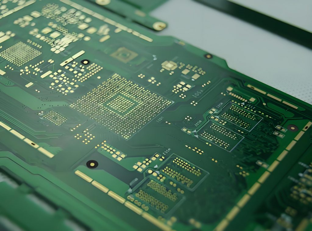
  • Carry out circuit design and layout planning based on design requirements and signal transmission characteristics.
  • Make PCB drawings and convert circuit layout and connection lines into circuit diagrams on the drawings.
  • The circuit diagram on the drawing is transferred to the substrate through photolithography technology and etched to form a conductive layer.
  • The film sticking process attaches the protective layer and copper clad layer to the conductive layer to protect the circuit and improve the mechanical strength.

3. ‌Welding and assembly process‌:

  • Surface mount technology is widely used in high frequency PCB welding, and SMT components are accurately welded to PCBs through methods such as hot air or reflow soldering.
  • Manual soldering technology also plays an important role in the assembly of high frequency PCBs. Plug-in components and connecting lines are connected by manual soldering.

4. ‌Special considerations for high frequency PCBs‌:

  • high frequency circuit design requires the adoption of special design principles and strategies, such as transmission line theory and matching, short and straight wiring strategies, impedance control and matching, decoupling and bypass, etc., to ensure signal quality and system reliability.
  • Adopt strategies such as multi-layer board design, straight wiring, shortening signal leads, reducing inter-layer alternation, being wary of crosstalk, increasing decoupling capacitors, isolating digital and analog ground wires, avoiding loops, ensuring impedance matching, and preventing ground bounce to improve Performance and reliability of high frequency circuits.
  • Through the above steps, a high-quality PCB that meets high frequency signal transmission requirements can be produced to ensure stable signal transmission and reliable operation of the system.

What are some important considerations when designing a PCB layout for high frequency circuits?

Designing high frequency PCB communication circuits faces many challenges and requires comprehensive consideration of circuit performance, electromagnetic compatibility, reliability and other aspects. Here are some of the major design challenges:

  • 1. Signal integrity: At high frequencies, signal transmission will be affected by reflection, crosstalk, attenuation and other factors, leading to signal integrity problems.
  • 2. Electromagnetic compatibility: As mentioned before, high frequency signals are prone to electromagnetic interference, so high frequency PCB communication circuits need to have good electromagnetic compatibility.
  • 3. Thermal management: high frequency PCB communication circuits will generate a large amount of heat when working. If the heat cannot be dissipated in a timely and effective manner, the performance of the circuit will be reduced or even damaged.
  • 4. Reliability: high frequency PCB communication circuits usually work in harsh environments, such as high temperature, high humidity, vibration, etc.

What is the highest frequency used for communication?

The highest frequency used for communication is 450GHz. ‌

What is a high frequency pcb communication circuits?

This frequency range was finally approved at the 2019 World Radiocommunication Conference (WRC-19) and involves the 275 GHz-296 GHz, 306 GHz-313 GHz, 318 GHz-333 GHz and 356 GHz-450 GHz frequency bands, for a total of 137 GHz Bandwidth resources.

These frequency bands are used without restrictions for fixed and land mobile service applications. This is the first time that ITU has clarified the spectrum resources available for terrestrial active radio service applications in the terahertz frequency band above 275 GHz, and raised the upper limit of available spectrum resources for active services to 450 GHz, providing basic resource guarantee for the development and application of the global terahertz communication industry. .

Which frequency is best for communication?

For WiFi communication, choosing which frequency band is best depends on the user’s specific needs and network environment.

  • The 2.4GHz frequency band is suitable for use in home and office environments because of its strong signal penetration and low interference, especially when wide coverage and signal stability are required.
  • Because of its high-speed transmission capabilities, the 5GHz band is suitable for scenarios that require large traffic transmission, such as high-definition videos and online games, because it provides faster network speeds and more stable transmission rates.

In satellite communications, different frequency bands have their own advantages and applicable scenarios.

  • Although the C-band has low frequency and low gain, its rain attenuation is much smaller than that of the Ku-band and even smaller than the Ka-band. It is suitable for businesses that have strict requirements on communication quality, such as television and radio.
  • The Ku band has high frequency, high gain, small antenna size, and is easy to install. It is especially suitable for mobile emergency communication services such as communication in motion and communication in silence, and satellite news collection SNG and DTH services.

When selecting the wireless communication frequency band bandwidth.

  • The 20MHz frequency band bandwidth is suitable for small to medium-sized wireless networks due to its stable signal and wide coverage.
  • Although the data transmission rate of the 40MHz band bandwidth is relatively high, the signal penetration capability is weak and is suitable for dense environments or application scenarios that require higher transmission rates.

What are examples of high frequency equipment?

high frequency PCB communication circuits are widely used in various fields. The following are some of the main application fields:

  • 1. Wireless communication: high frequency PCB communication circuits are the core components of wireless communication systems, such as mobile phones, base stations, satellite communications, etc.
  • 2. Radar system: high frequency PCB communication circuits are also widely used in radar systems, such as radar antennas, signal processing, transmitters and receivers, etc.
  • 3. Satellite communications: Satellite communications require the use of high frequency PCB communication circuits to transmit and receive signals.
  • 4. High-speed data transmission: In the field of high-speed data transmission, high frequency PCB communication circuits can achieve data transmission rates of tens of Gbps per second to meet the needs of large data volume and high bandwidth.

In short, high frequency PCB communication circuits are an important part of modern communication technology and have broad application prospects and development potential. With the continuous advancement of technology.

You may also like

PCB Surface Finish Lead-Free HASL
Thursday, September 19th, 2024

There are many different surface finishes used in the manufacturing of printed circuit boards (PCBs), of which HASL (Hot Air Solder Leveling) is a widely used technology.

What is HASL in PCB?

HASL is hot air solder leveling, which is a commonly used surface finish in the printed circuit board (PCB) industry.

HASL forms a coating that resists copper oxidation and provides good solderability by coating molten tin-lead solder on the surface of the PCB and using heated compressed air for leveling. This coating not only helps protect the copper from oxidation, but also ensures good soldering performance.

PCB Surface Finish Lead-Free HASL

There are two types of HASL: leaded and lead-free, making it one of the lower-cost PCB surface finishes. The leaded version was more common in the electronics manufacturing industry in the past, but with the improvement of environmental protection requirements, the lead-free version of HASL has also been widely used.

What is the difference between HASL and ENIG finish?

The main differences between HASL and ENIG surface finishes are their process flow, cost, corrosion resistance, applicable scenarios, and environmental protection. ‌

‌Process flow‌:

  • HASL (hot air leveling) is a traditional surface treatment process that provides good soldering performance by coating a layer of lead-tin alloy on the surface of the PCB.
  • ENIG (electro-nickel-gold) improves soldering performance and corrosion resistance by electroplating a thin layer of nickel and gold on the copper surface.

‌Cost‌:

  • HASL has a relatively low cost because it is a mature and widely used process.
  • In contrast, ENIG has a higher cost because it has stricter control requirements for the manufacturing process and uses higher material costs.

‌Corrosion resistance‌:

  • ENIG provides better corrosion resistance due to the presence of nickel and gold layers, especially for applications that require long-term reliability and stability.
  • Although HASL can also provide certain corrosion resistance, it is not as good as ENIG in terms of corrosion resistance.

‌Applicable scenarios‌:

  • HASL is suitable for most general applications due to its low cost and good soldering performance.
  • ENIG is more suitable for application scenarios with higher requirements for soldering performance and corrosion resistance.

‌Environmental protection‌:

  • HASL used to mainly use lead-containing materials, but with the restrictions of environmental regulations, lead-free HASL has gradually become the standard, but there are still potential environmental problems.
  • ENIG has no obvious environmental problems in this regard because it does not contain any hazardous substances.

In short, choosing HASL or ENIG depends on the specific application requirements, cost budget and environmental impact considerations. Each process has its unique advantages and applicable occasions. The right choice can significantly improve the performance and market competitiveness of multi-layer PCBs.

What is the difference between lead-free HASL and HASL?

The main difference between lead-free HASL and traditional HASL is the different materials used. ‌

PCB Surface Finish Lead-Free HASL

Traditional HASL (hot air leveling) uses lead-containing solder, which was once one of the most commonly used surface treatment technologies in electronic assembly.

However, due to restrictions on environmental regulations, lead-containing HASL has been gradually eliminated and replaced by lead-free HASL. Lead-free HASL uses non-lead metals or lead-free solder alloys to replace traditional lead-containing solder to meet environmental protection requirements.

The advantages of lead-free HASL include lower cost and good soldering performance. Compared with traditional HASL, lead-free HASL is more environmentally friendly and can pass environmental assessments such as RoHS certification.

However, the mechanical strength and glossiness of lead-free HASL may not be as good as traditional lead-containing HASL, and there may be some challenges in soldering fine components, especially in the case of poor surface flatness, which is easy to produce tin beads and short circuits for fine-pitch pin components. ‌

In general, lead-free HASL is an improvement on traditional HASL, with the main purpose of improving environmental performance. Although there may be some limitations in some aspects, it is currently a necessary choice to meet environmental regulations.

Is HASL with lead bad?

Lead-containing HASL is not an ideal choice because it has multiple disadvantages and limitations. ‌

First, the main disadvantages of lead-containing HASL include uneven surfaces, which are not suitable for fine-pitch applications.

PCB Surface Finish Lead-Free HASL

In addition, it faces problems of thermal shock and solder bridging, which may cause the plated through hole (PTH) to be blocked or reduced, as well as thickness/topography differences between large and small pads.

These problems make leaded HASL unsuitable for SMD and BGA with a pitch less than 20 mil, and unsuitable for HDI products and wire binding. Therefore, leaded HASL is gradually regarded as a suboptimal choice in modern electronic manufacturing.

Secondly, environmental protection is also an important consideration for leaded HASL. Due to environmental regulations, leaded versions of HASL have been gradually phased out in some areas, and lead-free HASL has become an alternative, but its soldering performance is slightly inferior to that of the leaded version.

Does HASL oxidize?

HASL (hot air leveling) does oxidize. ‌HASL protects the connection wires by coating a layer of tin-lead alloy, including anti-sulfurization treatment.

However, the surface flatness of HASL is relatively low, which may not be suitable for high-density, fine-pitch circuit design. In addition, due to the lead issue, the surface oxidation resistance of lead-free HASL is weak, and the long-term reliability is not as good as other advanced processes.

Therefore, although HASL provides some protection, it is not a complete solution to prevent oxidation, especially in long-term use or under certain environmental conditions, its protection effect may be affected.

Is HASL RoHS?

HASL is not RoHS compliant. ‌

HASL (hot air solder leveling) is a traditional PCB surface treatment process that contains lead (SnPb) solder. However, the RoHS (Restriction of Hazardous Substances) directive aims to restrict the use of certain hazardous substances in electrical and electronic equipment, specifically lead (Pb), mercury (Hg), cadmium (Cd), hexavalent chromium (Cr6+), polybrominated biphenyls (PBB) and polybrominated diphenyl ethers (PBDE).

Because the leaded solder used in the HASL process does not meet the RoHS standard for the restriction of hazardous substances, the traditional HASL process is not considered RoHS compliant. ‌

To meet RoHS standards, lead-free HASL (Lead-Free HASL) has become an alternative, which uses lead-free solder alloys such as tin-copper, tin-nickel or tin-copper-nickel alloy to replace traditional lead-containing solder.

Although lead-free HASL meets environmental requirements, it is not suitable for all situations, especially when dealing with fine-pitch components and dense wiring.

For projects that need to comply with RoHS standards, lead-free processing processes such as lead-free tin spraying or other RoHS-compliant surface treatment technologies should be given priority.

What is the best surface finish for PCB?

There are many surface treatment processes for PCBs, each with its specific advantages and applicable scenarios. The following are some common surface treatment processes and their characteristics:

  • ‌Hot Air Leveling (HASL): This is a traditional surface treatment method that is cost-effective and suitable for most general electronic products.
  • ‌Electroless Nickel Gold (ENIG): Especially suitable for PCBs with fine line spacing and high density, a layer of nickel is first deposited on the copper surface, and then a thin layer of gold is plated. The gold layer acts as a protective layer to prevent the nickel layer from oxidizing and provides long-term soldering reliability and good solderability.
  • ‌Organic solderability preservative (OSP)‌: An environmentally friendly and cost-effective surface treatment technology, especially suitable for low to medium complexity PCBs.
  • ‌Electroplating silver (immersion silver)‌: A layer of silver is deposited on the copper surface through a chemical reaction, providing excellent conductivity and solderability, and also has good corrosion resistance.

In summary, choosing the best surface treatment process requires comprehensive consideration of the specific needs, cost, and environmental factors of the product.

HASL, as a traditional PCB surface treatment process, has the advantages of good solderability, low cost, and wide applicability. In practical applications, it is necessary to select a suitable surface treatment process based on factors such as the type of PCB, the use environment, and environmental requirements.

You may also like

Ceramic PCB board, Low Volume&Customization
Wednesday, September 18th, 2024

In the field of electronics, ceramic circuit boards are quietly opening a new revolution with their unique charm and excellent performance. Ceramic circuit boards are gradually becoming the focus of the electronics industry, leading the industry to a more efficient, stable and advanced technological era.

What is a ceramic pcb board?

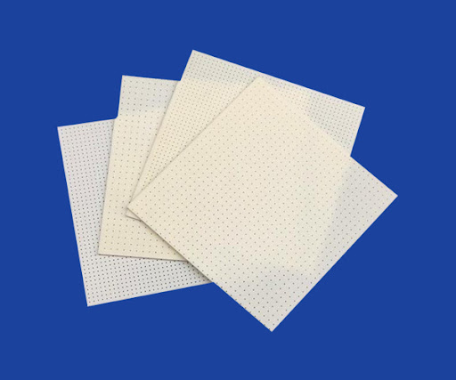
ceramic pcb board, also known as ceramic printed circuit board, is a printed circuit board that uses ceramic as a substrate instead of traditional fiberglass or epoxy resin. Compared with traditional substrates, ceramic materials have a variety of advantages, making them ideal for high-performance electronic applications.

Ceramic PCB board, Low Volume&Customization

What are the different types of ceramic PCB?

There are several types of ceramic materials commonly used in PCB boards, including aluminum oxide (Al₂O₃), aluminum nitride (AlN), and beryllium oxide (BeO). Each material has its own unique properties and advantages.

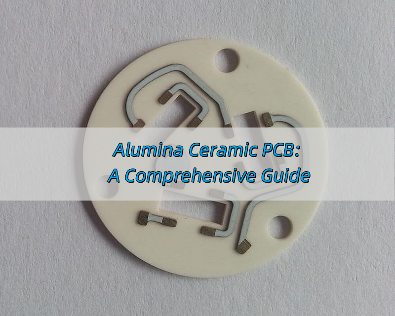
1. Alumina ceramic pcb board

Alumina is the most widely used ceramic material in PCB boards. It has excellent electrical insulation, high thermal conductivity and good mechanical strength. Alumina ceramic pcb boards are suitable for a wide range of applications, including power electronics, LED lighting and automotive electronics.

Ceramic PCB board, Low Volume&Customization

2. Aluminum Nitride ceramic pcb board

Aluminum nitride is a high-performance ceramic material with extremely high thermal conductivity. This makes it ideal for applications where heat dissipation is a key factor, such as high-power LEDs, power modules, and RF/microwave equipment.

3. Beryllium Oxide ceramic pcb board

Beryllium oxide is a highly toxic material, but it has excellent thermal conductivity and electrical insulation. Due to its toxicity, beryllium oxide ceramic pcb boards are only used in special applications where other materials cannot meet the performance requirements.

What is the high temperature ceramic PCB?

High temperature ceramic PCB‌ is a special ceramic circuit board designed for high temperature environments, commonly known as high temperature co-fired ceramic (HTCC) circuits. This circuit board is made by mixing adhesives, lubricants, solvents, plasticizers, and aluminum oxide to make raw ceramics, and then forming circuits.

The main feature of high temperature ceramic PCBs is their high temperature resistance, which allows them to work stably under extreme temperature conditions, making them ideal for applications that require high reliability and long-term stability.

In addition, during the manufacturing process of high-temperature ceramic PCB, the copper foil and the ceramic substrate are bonded together. This bonding method not only has strong bonding strength, but also the copper foil will not fall off, thus ensuring the performance stability in harsh environments such as high temperature and high humidity.

The materials of high-temperature ceramic PCB usually include ceramic materials such as aluminum oxide (Al2O3), beryllium oxide (BeO), aluminum nitride (AlN), silicon carbide (SiC) and boron nitride (BN). These materials are not only very effective in conducting heat, but also good electrical insulators, making high-temperature ceramic PCBs perform well in applications that require high thermal conductivity and excellent electrical properties.

In general, high-temperature ceramic PCB is a high-performance, high-reliability circuit board, especially suitable for applications that require high thermal conductivity, excellent electrical properties, and stable operation in harsh environments, such as aerospace, military electronics, etc.

What are the manufacturing processes involved in ceramic pcb boards?

The manufacturing process of ceramic pcb boards is more complicated than that of traditional PCB boards. It generally involves the following steps:

1. Substrate preparation

Ceramic substrates are prepared by sintering ceramic powder at high temperatures. The sintered substrate is then polished and cleaned to ensure a smooth surface for subsequent steps.

2. Circuit pattern formation

Circuit patterns are formed on ceramic substrates using various methods, such as screen printing, photolithography, or laser ablation. In screen printing, a conductive paste is printed onto the substrate to form a circuit pattern. Photolithography involves the use of a photomask and photoresist to create a circuit pattern. Laser ablation uses a laser to remove unwanted ceramic material to form a circuit pattern.

3. Metallization

After the circuit pattern is formed, the substrate is metallized to provide conductivity. This is usually done by sputtering or electroplating a thin layer of metal, such as copper or gold, onto the substrate.

4. Component mounting

Electronic components are then mounted onto the ceramic pcb board using surface mount technology (SMT) or through-hole technology (THT). SMT involves soldering components directly onto the surface of the PCB board, while THT involves inserting components into holes in the PCB board and soldering them to the bottom surface.

What are the advantages of ceramic pcb boards?

ceramic pcb boards have several advantages over traditional PCB boards, making them ideal for high-performance electronic applications. Some of the main advantages include:

  • 1. High thermal conductivity: Ceramic materials have excellent thermal conductivity, which allows for efficient heat dissipation.
  • 2. High electrical insulation: Ceramic materials have high electrical insulation, which reduces the risk of electrical short circuits and improves the reliability of electronic devices.
  • 3. Good mechanical strength: Ceramic materials have good mechanical strength, making them resistant to vibration and shock.
  • 4. Small size and light weight: ceramic pcb boards can be made very thin and lightweight, making them ideal for portable electronic devices.
  • 5. High-frequency performance: Ceramic materials have low dielectric losses and high frequency stability, making them suitable for high-frequency applications such as RF/microwave equipment.

What is a ceramic PCB used for?

Ceramic PCBs have a wide range of applications, including:

  • 1. Power Electronics: Ceramic PCBs are widely used in power electronics applications such as power modules, inverters, and converters. The high thermal conductivity and electrical insulation of ceramic materials make them ideal for handling high power levels.
Ceramic PCB board, Low Volume&Customization
  • 2. LED Lighting: Ceramic PCBs are used in LED lighting applications due to their excellent heat dissipation properties. The high thermal conductivity of ceramic materials helps to extend the life of LEDs by reducing operating temperatures.
  • 3. Automotive Electronics: Ceramic PCBs are used in automotive electronics applications such as engine control units, power steering systems, and airbag controllers. The high mechanical strength and reliability of ceramic materials make them suitable for use in harsh automotive environments.
  • 4. Aerospace and Defense: Ceramic PCBs are used in aerospace and defense applications due to their high performance and reliability. The small size and light weight of ceramic PCBs make them ideal for satellite and missile systems.
  • 5. Medical Devices: Ceramic PCBs are used in medical devices such as pacemakers, defibrillators, and hearing aids. The high electrical insulation and biocompatibility of ceramic materials make them suitable for use in medical applications.

How is ceramic pcb board developing?

As the electronics industry continues to develop, there is a growing demand for high-performance PCB boards that can meet the growing requirements of advanced electronic devices. ceramic pcb boards are expected to play an important role in meeting this demand. Some future trends in ceramic pcb board technology include:

1. Increased use of high-performance ceramic materials

As the performance requirements of electronic devices continue to increase, there is a growing demand for high-performance ceramic materials such as aluminum nitride and silicon carbide. These materials have higher thermal conductivity and electrical insulation than traditional ceramic materials, making them ideal for next-generation electronic devices.

2. Passive component integration

In order to reduce the size and weight of electronic devices, there is a growing trend to integrate passive components such as resistors, capacitors, and inductors onto PCB boards.

3. 3D printing of ceramic pcb boards

3D printing technology is emerging as a promising method for manufacturing ceramic pcb boards. 3D printing can create complex geometries and structures that are difficult to achieve using traditional manufacturing methods.

4. Development of hybrid PCBs

Hybrid PCBs that combine ceramic and traditional substrates are being developed. Hybrid PCBs can use ceramic substrates for the power section and traditional fiberglass substrates for the signal section.

Ceramic PCBs are a revolutionary technology that offers several advantages over traditional PCBs. As the electronics industry continues to grow, ceramic PCBs are expected to play an increasingly important role in meeting the growing demand for advanced electronic devices.

You may also like

Ceramic pcb, High Mixed&Customization
Wednesday, September 18th, 2024

In today’s era of rapid technological development, electronic devices have become an indispensable part of our lives. Behind this, a new type of circuit board material, ceramic pcb, is gradually becoming the most favored object in the field of electronics.

What is a ceramic pcb?

Ceramic circuit board, as the name suggests, is a circuit board made of ceramic as the substrate. Compared with traditional organic circuit boards, ceramic pcb have many unique advantages. Ceramic materials have extremely high heat resistance, insulation and mechanical strength, and can work stably under extreme environmental conditions.

Ceramic pcb Manufacturer, High Mixed&Customization

At the same time, ceramic pcb also have good thermal conductivity, which can effectively dissipate the heat generated by electronic components and improve the reliability and stability of electronic equipment.

Briefly describe the manufacturing process of ceramic pcb

The manufacturing process of ceramic pcbs is very complicated and requires multiple processes to complete.

First, it is necessary to select suitable ceramic materials, such as aluminum oxide, aluminum nitride, etc. These ceramic materials have different performance characteristics and can be selected according to specific application requirements.

Then, through precise processing technology, the ceramic material is made into the required shape and size. Next, advanced printing technology is used to print circuit graphics on the ceramic substrate.

Finally, through high-temperature sintering and other processes, the circuit pattern is fixed on the ceramic substrate to form a ceramic pcb.

What are the different types of ceramic PCB?

  • Alumina ceramic PCB:

Alumina ceramic PCB is one of the most commonly used types of ceramic PCBs in the current market. It has the advantages of low price, good thermal conductivity, high resistance, high hardness, high electrical insulation, strong corrosion resistance, and high biocompatibility.

Ceramic pcb Manufacturer, High Mixed&Customization

It is mainly used in white light, infrared, VCSEL LED lamps and other fields, usually used for 3W to 5W power LEDs. In the alumina PCB market, there are 75%, 96% and 99% alumina PCBs. The higher the purity, the better the performance, but the higher the cost.

  • Aluminum nitride ceramic PCB:

The thermal conductivity of aluminum nitride ceramic PCB is 7 to 10 times higher than that of alumina PCB. It has the advantages of high thermal conductivity and resistance, high hardness, high mechanical strength, high electrical insulation, strong corrosion resistance, high biocompatibility, and thermal expansion coefficient close to Si.

It is considered to be the most promising ceramic PCB in the future and is widely used in high-power LEDs, power modules, laser fields, etc.

  • Silicon nitride ceramic PCB:

Silicon nitride ceramic PCB has the advantages of high thermal conductivity, high strength, high fracture toughness, etc., and is mainly used in IGBT modules, vehicle modules, military industry, aerospace, aviation modules and other fields.

Unlike brittle traditional ceramic materials, at high temperatures, silicon nitride PCB has good mechanical strength and fracture toughness, and the thermal expansion coefficient matches that of Si. But the manufacture of silicon nitride PCB is not easy, the bonding of the circuit layer to the ceramic substrate is unstable, and the resistance and insulation are low.

  • Silicon carbide ceramic PCB:

Silicon carbide ceramic PCB has the advantages of good strength even at 1400°C, extremely high thermal conductivity and resistance, good semiconductor conductivity, high hardness, etc.

Mainly used in the laser field, it is easy to work at 1000°C. At present, the manufacturing cost of silicon carbide PCB is extremely expensive, but with the advancement of manufacturing technology in the future, it is expected to be more widely used.

What are the advantages of ceramic pcb?

  • 1. High thermal conductivity: Ceramic materials have good thermal conductivity and can effectively dissipate the heat generated by electronic components.
  • 2. High insulation: Ceramic materials have extremely high insulation properties, which can effectively prevent short circuits and leakage between circuits.
  • 3. High mechanical strength: Ceramic materials have high mechanical strength and can withstand large external forces and vibrations.
  • 4. Good dimensional stability: The thermal expansion coefficient of ceramic materials is very small, and they can maintain dimensional stability under different temperature environments.
  • 5. Good chemical stability: Ceramic materials have good chemical stability and can resist the erosion of various chemical substances.

What are the application areas of ceramic pcb?

  • 1. LED lighting: Since LED lamps generate a lot of heat when working, circuit boards with good thermal conductivity are needed to dissipate heat.
  • 2. Power electronics: Power electronic devices usually need to withstand high voltages and high currents, so circuit boards with good insulation and mechanical strength are needed.
  • 3. Aerospace: The aerospace field has very high requirements for the reliability and stability of electronic equipment, so it is necessary to use circuit boards with good heat resistance, insulation and mechanical strength.
  • 4. Medical equipment: Medical equipment has very high requirements for the safety and reliability of electronic equipment, so it is necessary to use circuit boards with good insulation and chemical stability.
  • 5. Communication equipment: Communication equipment has very high requirements for the high-frequency performance and stability of electronic equipment, so it is necessary to use circuit boards with good high-frequency performance and dimensional stability.

How thick is ceramic PCB?

The thickness of ceramic PCB varies depending on different types and application scenarios. Generally speaking, the thickness of common ceramic PCBs ranges from 0.25mm to 1.5mm.

Ceramic pcb Manufacturer, High Mixed&Customization

The thickness of alumina ceramic PCBs is usually 0.5mm – 1.5mm. Alumina ceramics are widely used because of their low cost, and the choice of board thickness usually depends on the specific application requirements.

In some occasions where space requirements are not high but a certain mechanical strength is required, thicker alumina ceramic PCBs may be selected, such as 1.2mm or 1.5mm thickness. In some small electronic devices with limited space, thinner alumina ceramic PCBs, such as 0.5mm or 0.8mm thickness, may be selected.

The thickness of aluminum nitride ceramic PCB is relatively thin, generally between 0.25mm – 1.0mm.

Aluminum nitride has better thermal performance, but it is also more expensive. Due to its high thermal conductivity, in some applications with extremely high heat dissipation requirements, such as heat dissipation substrates for high-power semiconductor chips, thinner aluminum nitride ceramic PCBs may be selected to achieve better heat dissipation and more compact design.

In some high-end electronic devices, aluminum nitride ceramic PCBs with a thickness of 0.5mm or 0.6mm may be used.

In short, the thickness of ceramic PCBs has a certain flexibility and can be selected according to specific application scenarios and performance requirements.

At what temperature does ceramic PCB melt?

Ceramic PCBs usually do not “melt” like metals.

Ceramic materials have very high melting points, such as the melting point of alumina ceramics is about 2050℃, and the melting point of aluminum nitride ceramics is about 2200℃. In the normal use environment of electronic equipment, ceramic PCBs will hardly reach such high temperatures.

It should be noted that although the ceramic PCB itself will not melt, the metal circuits, solder, etc. on it may change or be damaged at too high a temperature.

As an innovative treasure in the field of electronics, ceramic pcbs have many unique advantages and broad application prospects. It is believed that in the near future, ceramic pcbswill become the mainstream circuit board material in the electronics field and make greater contributions to the development of electronic technology.

You may also like

What are the ceramic pcb material?
Monday, September 16th, 2024

In this ever-changing era, electronic devices are changing our lives at an unprecedented speed. From smartphones to cars to industrial automation equipment, these products all hide an important component – ceramic printed circuit boards (Ceramic PCBs).

What are the commonly used materials for ceramic PCB substrates?

Imagine that in a tiny space, there are countless electronic components, which are closely arranged and interconnected to form a complex and sophisticated network. This is the working environment of ceramic PCBs. In order to ensure that these components can work normally under harsh conditions such as high temperature and high pressure, it is crucial to choose a suitable substrate.

Commonly used ceramic PCB substrates are mainly the following:

1. Alumina (Al2O3):

  • It is one of the preferred materials for its excellent insulation performance, good thermal conductivity and high mechanical strength.
What are the ceramic pcb material?
  • Alumina substrates are usually used to make single-layer ceramic PCBs, which are suitable for applications under medium temperature and pressure conditions.
  • It has extremely high chemical stability and is not easy to react with other substances, thus ensuring the long-term reliability of the circuit.

2. Aluminum nitride (AlN):

  • Compared with aluminum oxide, aluminum nitride has higher thermal conductivity and can dissipate heat more effectively, making it an ideal choice for manufacturing high-performance electronic products.
What are the ceramic pcb material?
  • Aluminum nitride substrates are often used to make double-layer or multi-layer ceramic PCBs, especially for high-frequency signal transmission and high power density applications.
  • In fields such as semiconductor packaging and LED lighting, the outstanding performance of aluminum nitride makes it one of the indispensable materials.

3. Silicon nitride (Si3N4):

  • It is known for its excellent heat resistance and chemical stability, and it still performs well in extreme environments.
  • Silicon nitride substrates not only have extremely high mechanical strength, but also can withstand a higher temperature range. They are widely used in demanding scenarios such as aerospace, automotive electronics and military equipment.

What are the commonly used conductor materials for ceramic PCBs?

Conductor materials play an extremely important role in ceramic PCBs. They are responsible for transmitting signals and electricity and are the link between various functional modules.

Common conductor materials include precious metals such as copper, gold, and silver, as well as nickel plating. Among them, copper is widely used for its good conductivity and affordable price; gold shines in high-end applications for its excellent corrosion resistance; silver is between the two, combining cost-effectiveness and reliability.

  • As the most commonly used conductor material, copper foil is soft enough to easily combine with ceramic substrates to form a durable circuit path.
  • Gold foil is mainly used in occasions that require high reliability and long life, such as aerospace, medical equipment, etc. The oxidation resistance and corrosion resistance of gold enable it to maintain stable electrical performance in extreme environments, ensuring the normal operation of key components.
  • Silver foil is widely used in mid- and low-end products due to its good conductivity and low cost. Silver’s conductivity is second only to gold, but it is more affordable in terms of cost and is suitable for large-scale production and application. In certain specific fields, such as high-frequency circuits and wireless communication equipment, silver foil can also play an important role.

What are the types of ceramic PCBs?

With the advancement of technology, ceramic PCBs have also developed into various types to adapt to various application scenarios:

1. Single-layer ceramic PCB:

  • Simple structure, low cost, suitable for occasions with low performance requirements.
  • This type of PCB usually has only one layer of ceramic substrate, on which a layer of conductor material is laid to form a basic circuit layout.
  • Single-layer ceramic PCBs are mainly used for entry-level electronic products, such as ordinary household appliances and basic communication equipment.

2. Double-layer or multi-layer ceramic PCB:

  • By stacking multiple layers of ceramic substrates and setting interconnection channels between them, more complex circuit designs can be achieved, which is suitable for high-end products that require high-density integration.
What are the ceramic pcb material?
  • This type of PCB can accommodate more electronic components and more complex circuit structures, and is widely used in high-performance computing, advanced medical equipment and high-end automotive electronic systems.
  • Multilayer ceramic PCBs have high design flexibility and can be customized according to specific needs to achieve optimal performance.

3. Hybrid ceramic PCB:

  • Combining ceramic substrates of different materials, giving full play to their respective advantages, suitable for use in special environments.
  • This type of PCB usually uses two or more ceramic materials, such as a combination of alumina and aluminum nitride, which can ensure good thermal conductivity and provide sufficient mechanical strength.
  • Hybrid ceramic PCBs are suitable for applications with extreme temperature changes and high pressure conditions, such as deep-sea exploration equipment and space exploration instruments.

Advantages and characteristics of ceramic PCB

The reason why ceramic PCBs stand out among many materials is inseparable from their unique advantages:

High temperature resistance:

  • It can remain stable at temperatures up to 1000℃, making it an ideal choice for high-temperature working environments.
  • Ceramic materials themselves have extremely high melting points and are not easy to deform or damage even under extremely high temperature conditions, which enables ceramic PCBs to operate reliably in extreme environments.

High reliability:

  • It will not deform or damage even under long-term exposure to extreme conditions, ensuring the continuous and reliable operation of the system.
  • Ceramic materials have high chemical stability and are not easy to react with other substances, so they can maintain stable electrical performance in harsh environments.

Excellent thermal management capabilities:

  • Efficient heat dissipation helps to extend the life of components and improve overall efficiency.
  • The high thermal conductivity of ceramic materials enables it to quickly conduct heat away, effectively reducing the temperature of the circuit board, thereby improving the reliability and service life of the system.

Environmentally friendly and pollution-free:

  • The production process meets green environmental protection standards and is easy to recycle and reuse after disposal.
  • The production process of ceramic PCBs produces less waste, and the discarded materials can be recycled, which is in line with the concept of sustainable development.

These characteristics make ceramic PCBs an important force in promoting scientific and technological progress, and continue to lead the industry to a higher level.

What are the applications of ceramic PCBs?

From aerospace to medical equipment, from automotive electronics to communication facilities, ceramic PCBs are everywhere.

In satellite navigation systems, ceramic PCBs ensure positioning accuracy with their reliable signal transmission capabilities; in medical devices such as pacemakers, they rely on their ability to accurately control current to protect patient safety. In addition, in the construction of 5G base stations, ceramic PCBs also play an irreplaceable role, supporting the demand for high-speed data transmission.

Specific application cases are as follows:

  • 1. Aerospace: In satellite communication systems, the high reliability of ceramic PCBs ensures the accuracy of data transmission. During long-term flight, ceramic PCBs can resist extreme temperature changes, maintain stable electrical performance, and ensure unimpeded communication between satellites and ground stations.
  • 2. Medical equipment: In implantable medical devices such as pacemakers, the miniaturization and high reliability of ceramic PCBs become key factors. Ceramic materials have good biocompatibility and will not have adverse effects on human tissues. At the same time, they can provide precise current control to ensure therapeutic effects.
  • 3. Automotive electronics: In modern automobiles, ceramic PCBs are widely used in key components such as engine control systems, sensors, and navigation systems. The high temperature resistance of ceramic PCBs enables it to operate reliably in high-temperature environments in the engine compartment, ensuring the safety and comfort of the vehicle.
  • 4. 5G communication: In the construction and maintenance of 5G base stations, the efficient heat dissipation capacity and high-density integration characteristics of ceramic PCBs make them an ideal choice. Ceramic PCBs can handle a large number of data transmission tasks and ensure the high-speed and stable operation of 5G networks.

What is the production process of ceramic PCB?

The production process of ceramic PCBs is very delicate, and every step needs to be strictly controlled to ensure the high quality of the final product.

  • 1. Raw material preparation: First, the required ceramic powder and other raw materials need to be prepared to ensure their purity and uniformity.
  • 2. Molding: The ceramic powder is made into a substrate by pressing or casting. The temperature and pressure need to be strictly controlled during the molding process to ensure the flatness and consistency of the substrate.
  • 3. Sintering: The formed substrate is placed in a high-temperature furnace for sintering. The sintering process requires precise control of the temperature curve to ensure the density and stability of the ceramic substrate.
  • 4. Metallization: A layer of conductor material such as copper, gold or silver is applied to the ceramic substrate by electroplating, spraying or other means. This process requires highly precise operation to ensure the uniform distribution and good adhesion of the conductor layer.
  • 5. Circuit design and etching: According to the circuit design drawings, etching is performed on the conductor layer to form the required circuit pattern. The etching process requires the use of special chemicals, and the time and temperature need to be precisely controlled to ensure the accuracy and clarity of the circuit pattern.
  • 6. Testing and inspection: Finally, the completed ceramic PCB is fully tested and inspected to ensure that its electrical and mechanical properties meet the design requirements. The test items include resistance, voltage, current and other indicators.

Through this series of fine process flows, ceramic PCBs have excellent performance and reliability and have become an indispensable part of the electronics industry.

What are the development trends and prospects of ceramic PCBs?

With the continuous advancement of science and technology and the growing social needs, ceramic PCBs are also constantly developing and improving. In the future, ceramic PCBs will show greater potential in the following aspects:

  • 1. Miniaturization and integration: As electronic products develop towards smaller and higher integration, ceramic PCBs will continue to shrink in size while accommodating more electronic components. This means achieving more complex functions in a limited space and improving the performance of the overall system.
  • 2. High performance and high reliability: In the future, ceramic PCBs will pay more attention to high performance and high reliability, especially in applications under extreme environments. The application of new materials and new technologies will further enhance the temperature resistance, mechanical strength and electrical stability of ceramic PCBs, enabling them to play a role in a wider range of fields.
  • 3. Environmental protection and sustainable development: As the global awareness of environmental protection increases, the production process of ceramic PCBs will pay more attention to environmental protection and sustainable development. The research and development and application of new environmentally friendly materials will become an important direction to reduce the impact on the environment.
  • 4. Intelligence and automation: Ceramic PCBs in the future will be more intelligent and automated. By introducing advanced manufacturing technology and intelligent control systems, production efficiency and product quality can be further improved, costs can be reduced, and market demand can be better met.

In short, as an advanced electronic material, ceramic PCBs have unique advantages and broad application prospects, making them an important force in promoting scientific and technological progress. With the continuous advancement of technology and changes in social needs, ceramic PCBs will continue to show greater potential and development space in various fields.

You may also like