What is the Pick and Place File for PCB Assembly?
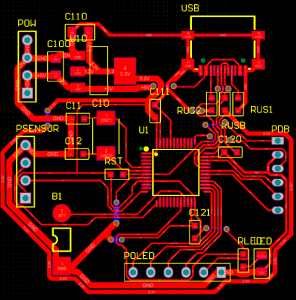
When assembling printed circuit boards, precise component placement matters a lot. That’s where the pick and place file in PCBA comes into play. This file lists each component’s location, orientation, and part number. It acts like a map that guides the machine responsible for placing components on the bare board. Without this data, machines have no clue where to position capacitors, resistors, or ICs.
The pick and place file, often called centroid file or XY data, acts as a bridge between the PCB design and the assembly process. It reduces human error, saves time, and boosts placement accuracy. Whether working on simple boards or complex multi-layer designs, this file makes the whole assembly process smoother and faster.

Why Does Pick & Place File Matter?
Every part on a PCB must land at the right spot. Even a minor offset can cause failures. The pick and place file ensures every component fits exactly where it belongs. It helps pick and place machines grab components and place them perfectly, following the designer’s plan.
Without this file, assembly teams would have to rely on manual placement or visual aids. That takes time and increases errors. Machines work faster, more consistently, and far more accurately than human hands. With a proper pick and place file, the machine knows the part number, package type, rotation angle, and X-Y coordinates for every single component.
This file also reduces the chances of missing parts or placing them upside down. When assembling hundreds or thousands of boards, even small mistakes add up. A clean, accurate file makes sure the entire batch meets quality standards, which is crucial for reliable products.
What is the Format of Pick and Place Machine File?
Most files use common formats, such as CSV (comma-separated values) or TXT (plain text). These work with nearly all pick and place machines, so manufacturers can share files easily across different platforms. The pick and place file in PCBA follows a simple structure that’s easy for machines and software to read. Though formats may vary slightly across design software, most include the following:
- Reference Designator – Marks each component, like R1 or U3.
- Part Number – Shows the specific part used.
- Package Type – Explains the physical size and shape, like 0402 or QFP.
- X Coordinate – Tells the machine the horizontal placement.
- Y Coordinate – Sets the vertical placement.
- Rotation Angle – Shows how the part should turn to match the footprint.
- Layer Information – Identifies if the part sits on the top or bottom side.
Pick and Place File Example
Here’s a simple pick and place file example to help visualize what it looks like:

This is just a small sample, but real files often contain hundreds or thousands of lines depending on the design complexity. Each line defines one component, ensuring machines have clear placement instructions.
How to Make a Pick and Place File?
Creating a pick and place file in PCBA starts in the design software. When laying out components, the software records the exact position, angle, and orientation for each part. Once the layout’s complete, the file can be generated directly from the software.
Steps generally follow this flow:
- Place all components and finalize the PCB layout.
- Label every part with clear reference designators.
- Assign correct part numbers and footprints.
- Check for correct orientation and ensure no components overlap.
- Export the pick and place file using the software’s built-in tools.
Good design habits, like keeping components aligned and properly spaced, also improve the file’s accuracy and make downstream processes smoother.
How to Generate Pick and Place File in Altium?
In Altium Designer, generating a pick and place file only takes a few steps. Altium makes the process intuitive, so designers don’t need extra plugins or manual tools. Here’s how it works:
- Open the PCB layout in Altium.
- Navigate to File > Assembly Outputs > Generate Pick and Place Files.
- Choose the top and bottom layers if needed.
- Select the output format (usually CSV or TXT).
- Review the preview to check for missing or misaligned parts.
- Save the file to the desired location.
Altium gives options to customize column order, units, and decimal precision. Double-checking these settings ensures the file works smoothly with the intended assembly equipment.
How to Export Pick and Place File?
The actual export process varies by software, but the core steps stay similar across most platforms. Here’s a general guide:
1. Open the completed PCB layout file.
2. Confirm all parts have correct designators, footprints, and placements.
3. Open the Output or Export menu (naming varies by software).

4. Choose Pick and Place File or Centroid File from the list and export.

5. Select output preferences — file type, units, layers, etc.

6. Review the file for missing data before saving.
Most tools let designers export top and bottom placements separately or combined. Always double-check orientation and rotation values since errors here cause misaligned parts during assembly.
How to Generate Pick and Place File from Gerber?
Gerber files mainly handle copper, solder mask, and silkscreen layers — they don’t directly hold placement data. However, some design tools can extract placement data if the Gerbers contain embedded component data, which isn’t common.
If placement data isn’t embedded, the best approach is to return to the original PCB design file. Most PCB CAD software (like Altium, KiCad, or Eagle) can regenerate a pick and place file directly. If the original design file is unavailable, creating a new placement file requires manual work — identifying parts from the silkscreen and manually recording coordinates.
What is the Pick and Place Process?
The pick and place process starts after the bare PCB arrives at the assembly line. Machines read the pick and place file to know exactly where each component should go. Here’s a simplified version of the steps:
1. Preparing the PCB
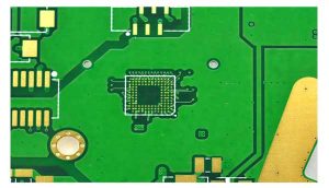
Prepare the bare PCB carefully before the assembly process starts. Full inspection is needed to check for defects, scratches, or contamination. For PCBs stored for a long time, baking is important to remove moisture, which helps avoid soldering issues later. After that, solder paste is applied to the pads where components will sit.
2. Feeding the Components
Next, components get loaded into the machine through feeders. These feeders hold reels, trays, or sticks of parts, all arranged in order. Each component type has its own feeder position, linked to the pick and place file.
3. Picking Up Components
The machine starts by picking up components from the feeders using vacuum nozzles. Each nozzle is designed to handle a specific part size, from tiny resistors to larger ICs. The machine uses gentle suction to grab each component without damaging it.
4. Vision Inspection and Alignment
After picking up each component, the machine checks its orientation using a vision system. High-resolution cameras take images to see if the part is facing the right way. If there’s any slight misalignment, the machine rotates the part to the correct angle before placement.
5. Placing Components on the Board
Once the part is aligned, the machine places it onto the PCB. Each component is placed at the exact coordinates provided in the pick and place file. The machine also adjusts the rotation angle to match the footprint on the board. Parts are placed carefully with the right amount of pressure to avoid damaging delicate parts or shifting the solder paste.
6. Speed and Precision Combined
Pick and place machines combine high speed with extreme precision. Modern machines can place thousands of parts per hour, even at microscopic sizes. While speed matters, accuracy is even more important. Each placed component must sit perfectly on its pad, since even the smallest shift could cause electrical issues after soldering.
7. Handling Different Part Sizes
Pick and place machines handle a wide range of components, from tiny 0201 resistors to large connectors. The machine automatically switches nozzles based on the part size.
8. Real-Time Monitoring
Throughout the process, the machine monitors everything in real time. Sensors track part pick-up, alignment checks, and placements. If a feeder runs empty or a part fails inspection, the machine pauses and alerts the operator.
9. Final Transfer for Soldering
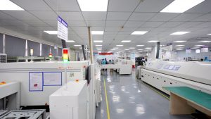
Once all parts are placed, the PCB moves to the next step — reflow soldering. The solder paste melts during this stage, permanently bonding each component to the board. Accurate placement during the pick and place process helps ensure every connection forms correctly, which supports good electrical performance in the final product. Here is a full manufacturing process of PCB assembly:
In short, the pick and place process bridges the gap between PCB design and working hardware. It translates design data into real, physical assemblies — fast, accurately, and reliably. Without it, modern electronics manufacturing wouldn’t be able to meet today’s high standards for quality and volume.
At Best Technology, our pick and place process combines high-speed machines, careful file preparation, and experienced operators. Our team knows how important clear placement data is for delivering high-quality PCBs. If you’re looking for reliable PCB assembly services or want help preparing your files, feel free to reach out. We’ll make sure your designs turn into top-quality products, every time.


