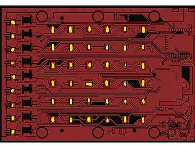
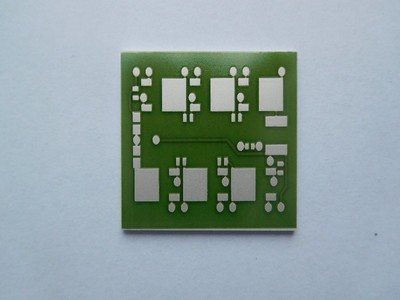
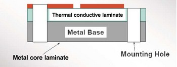
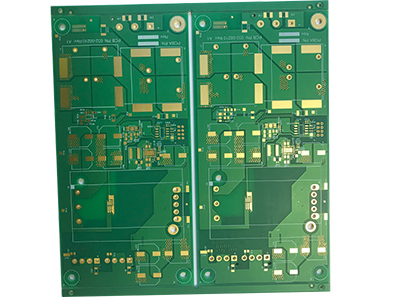
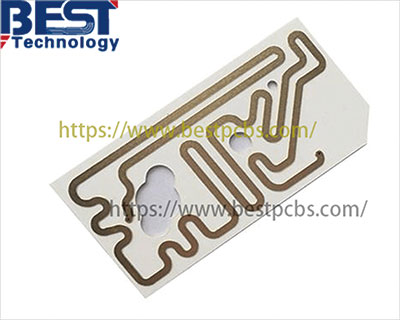
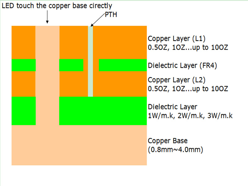
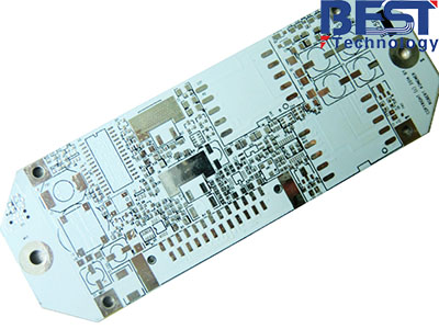
About the SinkPad copper core PCB, all is known that convexity is very important, the height of convexity is about 0.2mm-0.25mm.
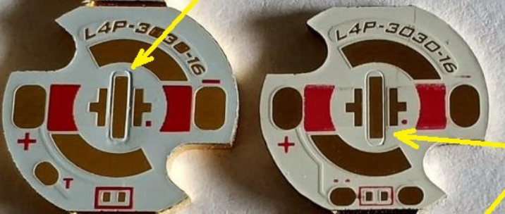
We need to know what’s the reasons caused the gap between the convexity and LED pad is big.
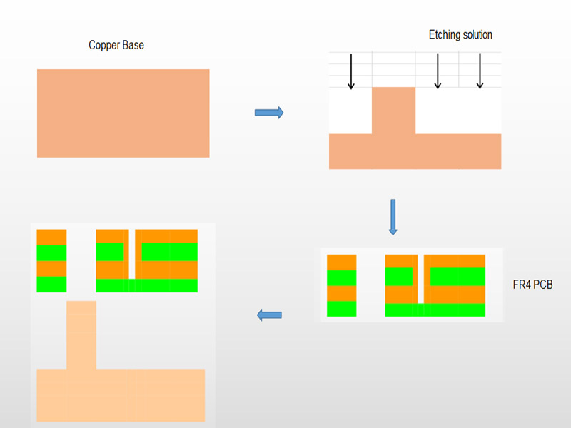
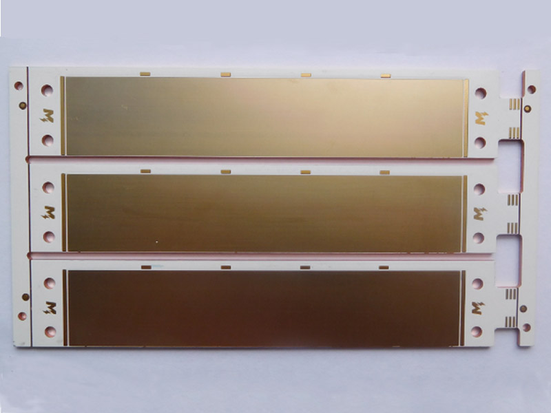
- We make the copper core with convexity firstly, then make the circuit/panel board (FR4PCB/BT PCB) and finally do the lamination for cooper core and circuit board.
- The tolerance for convexity is +/-0.05mm-0.075mm.
- The tolerance for circuit/panel board is +/-0.13mm.
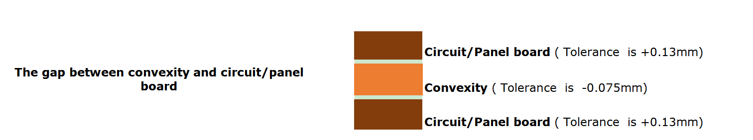
If we do negative tolerance for convexity and positive tolerance for circuit/panel board, then it will cause the gap very big.
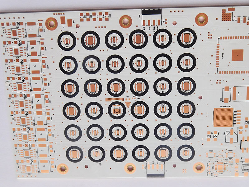
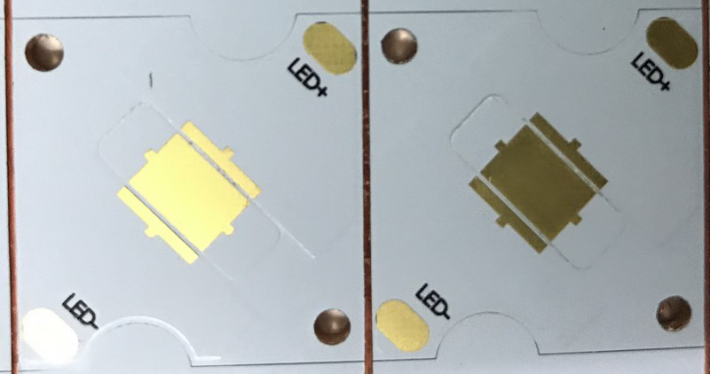
See below picture and details.
For example, the size of convexity is 0.5mm, after negative tolerance -0.075mm, it will be 0.425mm and each side will be 0.0375mm smaller.
For the circuit/panel board, the gap between convexity is 0.2mm, after positive tolerance +0.13mm, it will be 0.33mm and each side will be 0.065mm bigger.
So finally, the gap will be 0.2mm+0.0375+0.065mm=0.3025mm. It is about 50% bigger than original size.
How to improve that problem?
- Making the copper core with convexity according to design.
- Measuring the dimension of convexity before making the circuit/panel board, then making the circuit/panel board according to the convexity dimension with compensation design.
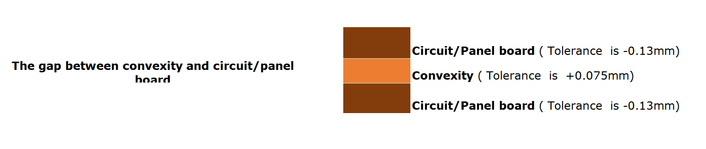
- Do Positive tolerance for convexity and negative tolerance for circuit/panel board, the gap will be much more smaller.
For example, the size of convexity is 0.5mm, after negative tolerance +0.075mm, it will be 0.575mm and each side will be 0.0375mm bigger
For the circuit/panel board, the gap between convexity is 0.2mm, after positive tolerance -0.13mm, it will be 0.07mm and each side will be 0.065mm smaller.
So finally, the gap will be 0.2mm-0.0375-0.065mm=0.0975mm. It is about 50% smaller than original size.
For more information about SinkPad PCB, please click
https://www.bestpcbs.com/products/multi-layer-sinkpad-board.htm