pcb
Home > Blog

Posts Tagged ‘SMT’

What is a PCB assembly?
Thursday, August 22nd, 2024

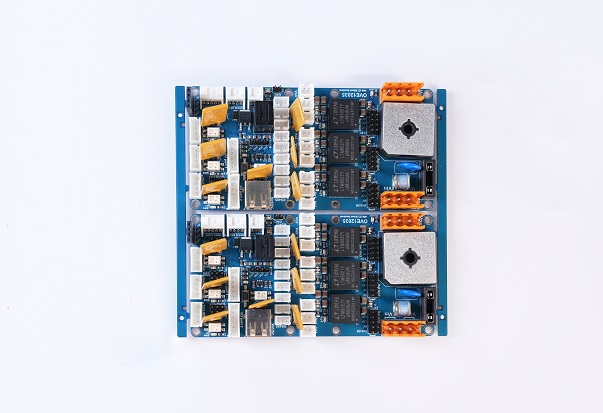
PCB assembly is the process of combining a circuit board with other electronic components (such as connectors, housings, heat sinks, etc.) to embed into a final product. This process is a key step in the production of electronic equipment. Its main function is to provide a platform for electronic components to work together in a coordinated manner so that the equipment can perform its intended tasks.

What is the standard for PCB assembly?

The standards for PCB assembly mainly include PCB panel specifications, ISO standards, IPC standards, JEDEC standards, and ROHS standards. ‌

What is a PCB assembly?

‌PCB panel specifications‌ involve the width, shape, frame design, center distance between small boards, setting of positioning holes, arrangement of reference symbols, and positioning of large components of the panel. The panel frame should adopt a closed-loop design to ensure that the panel is fixed on the fixture without deformation.

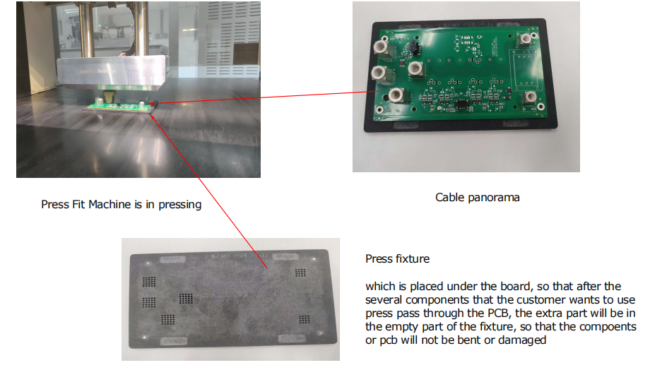
‌ISO standards‌ emphasize key factors such as fit tolerance, surface roughness, contact area, and tightening force in PCB tight-fit installation to ensure the accuracy and stability of installation‌.

‌IPC standards‌ include IPC-7711 and IPC-A-600E, the former provides basic recommendations and guidelines for the design and manufacture of printed boards, and the latter provides acceptable conditions and practice guidelines for printed boards.

‌JEDEC standards‌ provide specifications for circuit board materials, dimensions, interfaces, etc., including material selection, dimension design, interface specifications, test methods and quality assurance.
‌ROHS standard‌ is a directive on the restriction of the use of hazardous substances, aimed at reducing the impact on the environment and human health. It stipulates the use restrictions of hazardous substances such as lead, mercury, cadmium, hexavalent chromium, polybrominated biphenyls and polybrominated diphenyl ethers.

Compliance with these standards ensures the quality, safety and environmental friendliness of PCB products, and also provides clear guidance and specifications for the design, manufacture and assembly of PCBs.

Why is PCB assembly so expensive?

The high cost of PCB assembly is mainly due to the combined influence of multiple factors. ‌

First, the production cost of PCB boards is affected by materials, design and manufacturing complexity, precision and quality, and supply chain and regional differences. PCB boards are mainly made of materials such as copper, fiberglass and epoxy resin, and the cost of these materials directly affects the price of PCB boards.

The complexity of the design and manufacturing process, including pre-processing, image transfer, electroplating, etching, inspection and trimming, and post-processing, requires precise tools and professional skills, which will also be reflected in the cost. High-precision PCB boards require higher manufacturing costs because they require more precise tools and more stringent manufacturing processes.

Details in the PCB assembly process, layer selection, and the application of HDI technology will all have an impact on the cost. Every small change may cause the cost to plummet, so if you want to save money without losing performance, you need to consider these factors comprehensively.

In addition, the welding process is also a costly link. Soldering is a key step in fixing electronic components to PCBs. This process requires heating each joint separately for welding, which is a slow and laborious process.

Finally, the price of PCBs is also affected by factors such as materials, surface processing, design standards, copper foil thickness, quality acceptance standards, and mold fees and test frames. For example, different materials, surface processing, and copper foil thickness will lead to price differences.

In summary, the high cost of PCB assembly is mainly due to the combined effect of multiple factors such as material cost, manufacturing complexity, precision and quality requirements, production needs, and specific design and quality requirements.

What does PCB stand for?

PCB stands for Printed Circuit Board. ‌

What is a PCB assembly?

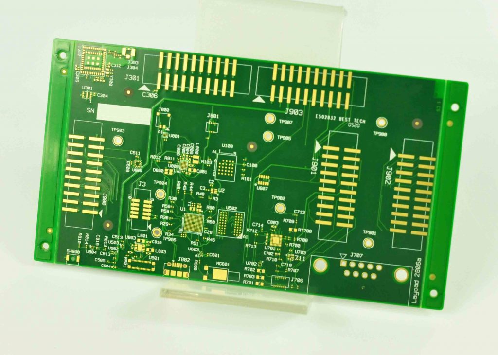
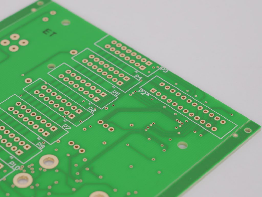
Printed circuit board (PCB), also known as printed circuit board, is an indispensable component in electronic engineering. It is the support of electronic components and also the carrier of electrical connection of electronic components.

Printed circuit boards are widely used in various electronic devices. Printed circuit boards can be divided into single-sided boards, double-sided boards, multi-layer boards, etc. according to the number of layers of circuit boards. Among them, multi-layer boards refer to printed boards with more than two layers. It consists of connecting wires on several layers of insulating substrates and pads for assembling and welding electronic components. It has the function of conducting each layer of circuits and insulating each other.

The wide application of printed circuit boards makes it possible to miniaturize and visualize the circuits of electronic devices, which plays an important role in the mass production of fixed circuits and optimizing the layout of electrical appliances. This type of circuit board uses polyimide or polyester film as the substrate, and has the characteristics of high wiring density, light weight, thin thickness and good bendability.

What is the difference between PCB and PCBA?

The main difference between PCB and PCBA lies in their definition, function, application and manufacturing process. ‌

Definition:

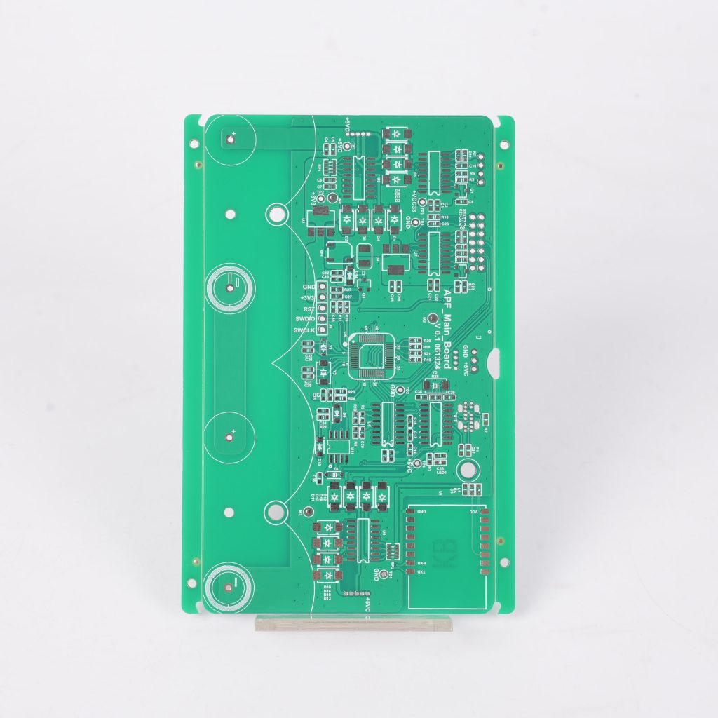
PCB (printed circuit board) is a basic electronic component made by electronic printing, mainly used as a support for electronic components, and does not contain any active or passive components.

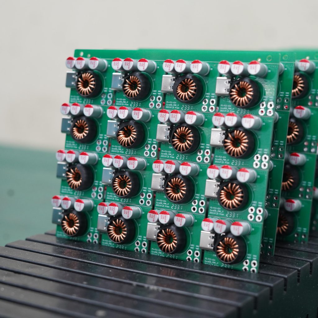
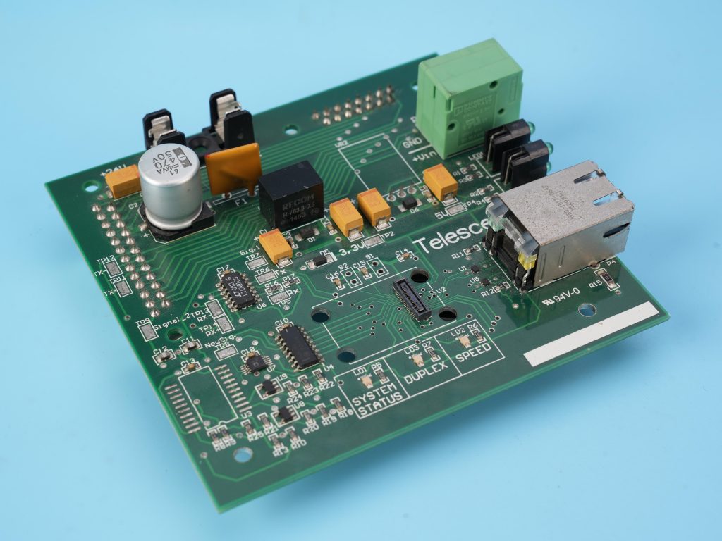
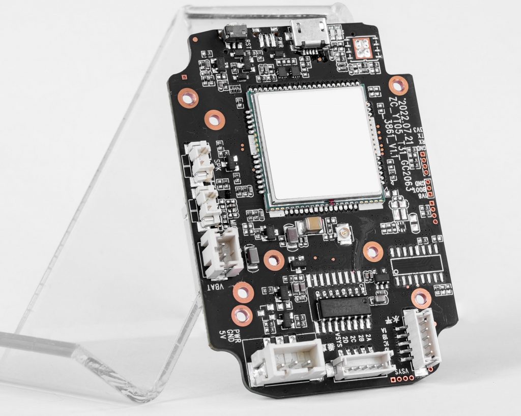
PCBA (printed circuit board assembly) is a circuit board assembly with specific functions formed by soldering electronic components to PCB through processes such as SMT (surface mount technology) or THT (through-hole mounting technology). PCBA contains PCB and all necessary electronic components, which work together to realize the preset functions of the circuit board.

What is a PCB assembly?

‌Function and application‌:

The main function of PCB is to support and connect electronic components, while PCBA integrates electronic components into a complete circuit system, which can be used in the manufacture of various electronic products.

PCBA is the core part of electronic products and directly determines the performance and function of the product.

‌Manufacturing process‌:

The manufacturing process of PCB includes circuit design, PCB board design, PCB template production, copper foil etching, drilling, tin spraying and board making.

The production of PCBA requires component mounting, welding, testing and other processes.

In summary, the main difference between PCB and PCBA lies in their definition, function, application and manufacturing process. PCB is a basic electronic component, mainly used to support and connect electronic components, while PCBA is a finished product formed by welding electronic components to PCB. It has specific circuit functions and is an indispensable part of electronic products.

What is the difference between PCB manufacturing and assembly?

The main difference between PCB manufacturing and assembly is that they involve different processes and focuses. ‌

‌PCB manufacturing‌ mainly involves the process of converting raw materials into printed circuit boards through a series of process flows, including design, layout, etching, lamination, drilling, welding and other steps, and finally forming a complete and usable printed circuit board.

‌PCB assembly‌ is the process of soldering electronic components to the printed circuit board according to the design requirements after the PCB is manufactured. The focus of assembly is to ensure that all components are in the correct position and direction, the pins of each component are fully soldered to the designated pads, and there is no excess solder or other excess materials to ensure the normal operation and reliability of the circuit board.

In short, ‌manufacturing‌ covers the entire production process from raw materials to finished products, including design, production and testing, while ‌assembly‌ is a link in the manufacturing process that focuses on accurately mounting electronic components on printed circuit boards to ensure the final function and performance of the product.

Conclusion:

PCB assembly is an important part of manufacturing and affects the quality of the final product. Therefore, choosing the right manufacturer becomes particularly important. BEST Technology is committed to becoming the world’s most trusted one-stop electronic circuit solution provider, while focusing on PCBA prototyping and small batch production. Choosing us will get the best quality products.

You may also like

what is glass transition temperature?
Wednesday, August 21st, 2024

In the PCB manufacturing process, the glass transition temperature is an important performance indicator. During the manufacturing and use of PCB boards, they will undergo multiple heating and cooling processes. If the operating temperature exceeds the glass transition temperature, the board will soften, expand, or even deform, affecting the accuracy and reliability of the circuit. Therefore, choosing the right glass transition temperature is crucial to ensure the dimensional stability and long-term performance of the PCB.

What is the glass transition temperature and Its Significance?

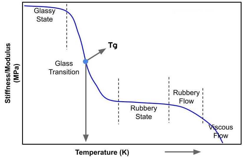
The glass transition temperature (Tg) refers to the temperature corresponding to the transition from the glass state to the high elastic state. The glass transition is an inherent property of amorphous polymer materials and a macroscopic manifestation of the transformation of the polymer motion form. It directly affects the performance and process performance of the material. Therefore, it has long been the main content of polymer physics research.

what is glass transition temperature?

The glass transition temperature is of great significance to the application of polymers. Above this temperature, polymers show elasticity; below this temperature, polymers show brittleness. This characteristic must be considered when used as plastics, rubber, synthetic fibers, etc.

The glass transition temperature of mainstream FR-4 boards is approximately between 130-140℃. In the PCB manufacturing process, the temperature needs to be strictly controlled to avoid exceeding the glass transition temperature to ensure the quality of the product.

Is higher glass transition temperature better?

In PCB manufacturing, the higher the glass transition temperature (Tg), the better. ‌

what is glass transition temperature?

The glass transition temperature is an important performance indicator of polymer materials, which determines the changes in the physical and chemical properties of the material at a specific temperature. When the temperature of the polymer is lower than its glass transition temperature, the material exhibits hard and brittle characteristics, similar to the glass state; when the temperature is higher than the glass transition temperature, the material becomes soft and exhibits elasticity similar to rubber or leather. This state change has a direct impact on the performance during PCB manufacturing and use.

1. ‌ Temperature deformation resistance ‌:

The higher the Tg value, the stronger the material’s temperature deformation resistance. This means that in a high temperature environment, such as during SMT welding, the PCB substrate is not easy to deform, thereby maintaining dimensional stability, which is crucial to ensure the reliability and long-term use of the circuit board.
2. ‌ Electrical performance and mechanical strength: ‌

The high or low Tg value directly affects the electrical performance and mechanical strength of the PCB. High Tg materials can maintain good physical and chemical stability at high temperatures, thereby maintaining the electrical properties and mechanical strength of the circuit board, which is crucial to improving the quality and reliability of the product.

3. Safety:

PCB materials with high Tg values ​​are not easy to soften or melt at high temperatures, thereby improving the safety and durability of the circuit board and reducing the risk of short circuits or other damage caused by high temperatures.

In summary, choosing PCB materials with higher Tg values ​​is one of the key factors to ensure that the circuit board maintains stable performance and safety in complex manufacturing and use environments.

What is glass transition temperature vs melting temperature?

In PCB manufacturing, glass transition temperature and melting temperature are two different physical properties that describe the state changes of materials under different conditions. ‌

The glass transition temperature (Tg) mainly involves amorphous materials or amorphous regions in partially crystalline materials. At this temperature, the physical state of the material changes from glass to highly elastic.

The melting temperature (melting point) mainly involves the melting process of crystalline materials. For crystalline polymers, the melting point marks the temperature at which the molecular chain begins to move, that is, the material changes from solid to liquid. The melting point is related to the crystallinity and lattice structure of the material and is a physical property unique to crystalline materials.

In short, the glass transition temperature mainly affects the amorphous region in amorphous or partially crystalline materials, while the melting temperature mainly affects crystalline materials and involves the melting process of the entire crystal. These two temperatures reflect the different physical state changes of different materials when heated.

How do you determine the glass transition temperature?

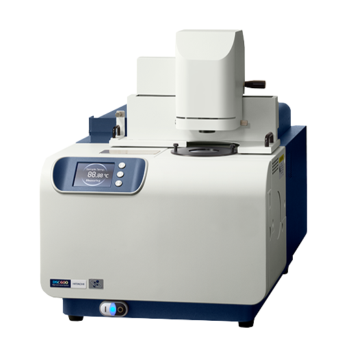
Expansion method, thermomechanical method, differential scanning calorimetry (DSC), DTA method, dynamic mechanical property analysis (DMA) method, nuclear magnetic resonance method (NMR).

what is glass transition temperature?

Differential scanning calorimetry (DSC) is the most traditional and commonly used measurement method. It measures the relationship between the power difference (heat flow rate) and temperature between the sample and the reference material, and then obtains the glass transition temperature of the material;

Dynamic mechanical analysis (DMA) is the most sensitive method. It measures the sinusoidal alternating stress of constant amplitude applied to the sample, observes the change of strain with temperature or time, and calculates the mechanical parameters to characterize the elastomer;

Thermomechanical analysis (TMA): Use a probe with good sensitivity to measure the expansion coefficient of the material, and measure the glass transition temperature of the material based on this change.

What is the difference between TM and Tg?

In the PCB industry, TM and Tg are two different parameters, representing two different physical properties.

Tm: melting point; m is the melting point of crystalline polymers, that is, the temperature at which crystalline polymers melt. It is the highest use temperature of crystalline polymers when used in plastics and fibers, and it is also their heat resistance temperature and the lowest temperature for molding processing.

What is the Tg of polyurethane?

The glass transition temperature (Tg) of polyurethane is not a fixed value, but a physical quantity determined by the type of resin.

‌There are many types of polyurethane, including polyether, polyester, polyimide, polyurea, etc. Each type of polyurethane has its own specific glass transition temperature.

Shape memory polyurethane has a small volume expansion rate at temperatures below Tg, but increases at temperatures above Tg, which shows the characteristics of its glass transition temperature. Therefore, to determine the glass transition temperature of a specific polyurethane, its specific chemical structure and application field need to be considered.

What is Tg for epoxy?

The Tg value of PCB epoxy resin is usually between 130℃ and 170℃. ‌

The Tg value (glass transition temperature) of PCB (printed circuit board) epoxy resin is an important performance indicator, which reflects the change in the physical state of the material when heated. According to different application requirements, the Tg value of PCB epoxy resin can be divided into several grades:

what is glass transition temperature?

‌TG130‌: The temperature resistance of this type of board is about 140℃. Common Tg value boards of this type are Shengyi S1141 and Jiantao KB-6164F.

TG150: A medium Tg board with a temperature range of 150°C to 170°C. Common boards with this type of Tg include Shengyi S1141 150 and Jiantao KB-6165F.

TG170: A high Tg board with a temperature range of over 170°C. Common boards with this type of Tg include Shengyi S1170 and Jiantao KB-6167F.

Selecting the right Tg value is critical to ensuring the performance and reliability of the PCB. Although boards with high Tg values ​​are relatively expensive, their superior temperature resistance is indispensable in applications that require higher temperatures, such as aerospace. In addition to Tg values, other factors should be considered when selecting PCB boards, such as thermal decomposition temperature (Td), which is another important indicator for evaluating the stability of boards at high temperatures.

Conclusion:

High Tg represents high heat resistance. Electronic products represented by computers are developing towards high functionality and high multi-layer, which requires higher heat resistance of PCB substrate materials as an important guarantee. BEST Technology focuses on manufacturing high-performance PCB circuit boards and is far ahead in the industry. It has professional production equipment and 18 years of design experience, and has high quality requirements for products.

You may also like

Understanding Press-Fit Technology in PCB Surface Mount Technology (SMT)
Friday, August 16th, 2024

What is Press-Fit Technology?

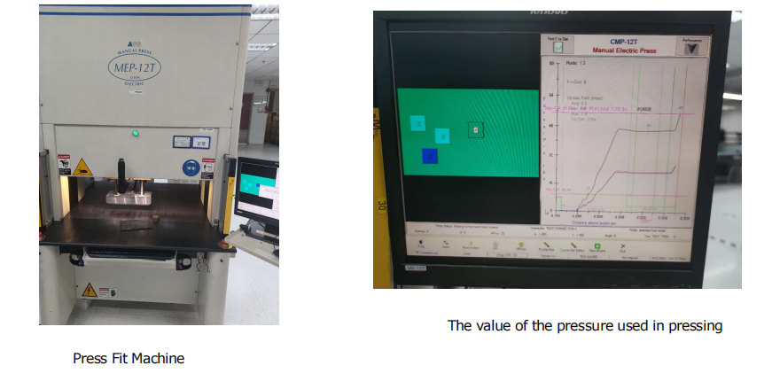
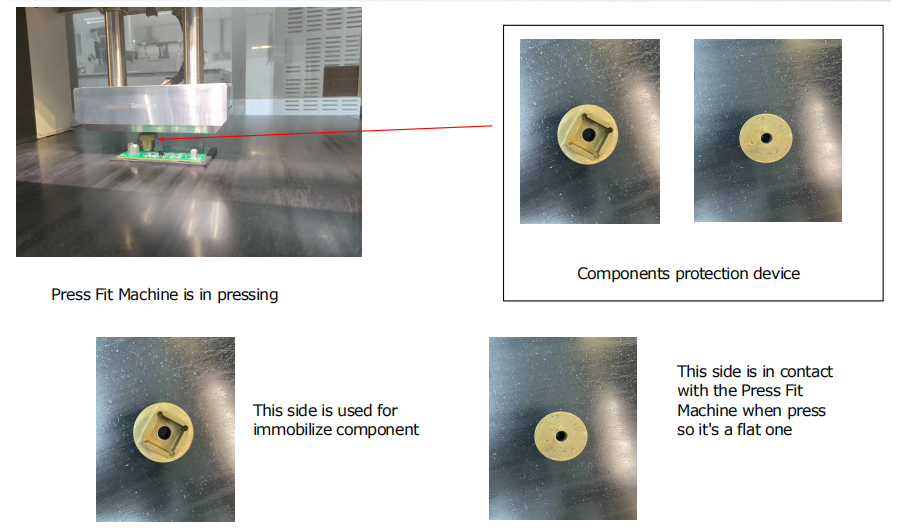
Press-Fit technology is a solderless connection method used to install connectors, pins, or other components into a PCB. The components have specially designed pins that are slightly larger than the PCB’s plated through-holes (PTH). These pins are pressed into the holes with sufficient force, creating a secure and reliable mechanical and electrical connection through compression.

The key feature of this technology is that it eliminates the need for soldering. Instead of using heat and solder to establish the connection, the mechanical force ensures that the contact between the pin and the wall of the hole is firm enough to create a stable electrical pathway. This method offers high durability and is especially useful in environments where temperature fluctuations, vibrations, or mechanical stress are present.

Understanding Press-Fit Technology in PCB Surface Mount Technology (SMT)

Advantages of Press-Fit Technology in SMT

1. No Heat Damage

Traditional soldering processes expose components to high temperatures, which can sometimes damage sensitive parts. Press-Fit technology avoids this by using a mechanical press to insert the pins, preserving the integrity of temperature-sensitive components.

2. High Reliability

The press-fit connection creates a strong and stable bond, even in challenging environments such as automotive and industrial applications. The mechanical compression between the pin and the hole ensures excellent electrical contact without the risk of thermal cycling or solder joint cracking over time.

3. Maintenance and Repair

One of the significant advantages of Press-Fit technology is its ease of repair. Since the connections are mechanical rather than soldered, they can be easily removed or replaced if needed without damaging the PCB or the component.

4. Environmental Benefits

By eliminating the need for solder and flux, press-fit technology is also a more environmentally friendly solution. This method reduces the use of hazardous materials and can help meet stricter environmental standards

Application of Press-Fit in SMT

In our SMT assembly process, Press-Fit technology is typically applied to connectors and other components that require robust, high-density connections. This technology is particularly popular in automotive electronics, telecom infrastructure, medical devices, and other high-reliability sectors.

Press-Fit connectors are also ideal for multi-layer PCBs, where a strong and stable connection is essential across various layers of circuitry. By using this technology, we ensure that our products meet the highest standards of performance and durability, especially in critical applications where failure is not an option.

Press-Fit technology is a critical component of modern SMT assembly, providing a highly reliable, solderfree connection method. Its mechanical strength, ease of maintenance, and suitability for harsh environments make it a preferred choice for various high-demand applications. As electronics continue to advance, Press-Fit technology offers a robust and environmentally friendly solution to meet the needs of the industry

You may also like

How to Make SMT? What is SMT Process?
Thursday, August 15th, 2024

What is the SMT?

Surface Mount Technology (SMT) is a production technique used to attach electronic components directly onto the surface of a printed circuit board (PCB). This method enables automated manufacturing to handle most of the assembly process needed to create a functioning board. Components attached in this way are known as surface-mount devices (SMDs). Unlike traditional methods, SMT does not involve inserting components through holes in the board. Instead, components are soldered directly onto the surface using reflow soldering.

Originally known as Planar Mounting, SMT was pioneered by IBM in the 1960s for small-scale computer production, replacing the earlier Through-Hole Technology. However, SMT didn’t gain widespread use until 1986, when surface-mounted components achieved 10% market penetration. By 1990, SMDs had become a dominant feature in most high-tech circuit card assemblies (CCAs).

How to Make SMT? What is SMT Process?

What is the process of SMT manufacturing?

The SMT manufacturing process can be divided into three main stages: solder paste printing, component placement, and reflow soldering. Due to the complexity of the process, each stage is further broken down as follows:

1. Component and PCB Preparation

This initial stage involves selecting surface-mount components (SMCs) and designing the PCB. The board typically features flat copper pads plated with silver, tin-lead, or gold, which are called solder pads. These pads do not have holes and are used to support the pins of components like chips and transistors.

Another crucial element is the stencil, which is aligned with the solder pads to define the placement of solder paste during the next stage. The PCB and all materials involved must be thoroughly inspected to ensure there are no defects before proceeding with production.

2. Solder Paste Printing

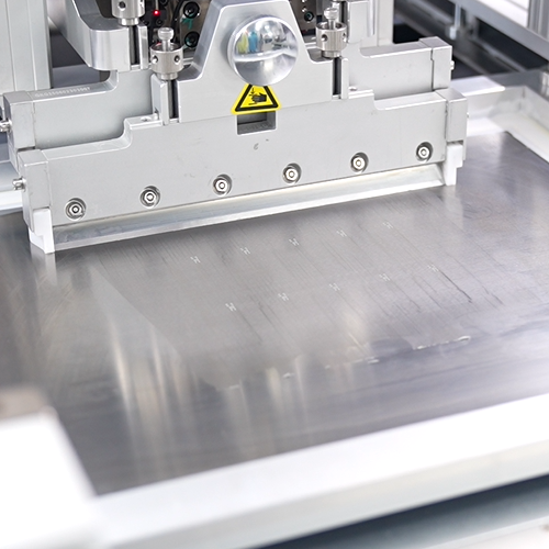
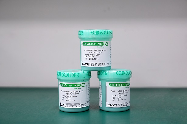
Solder paste printing is a critical phase in SMT production. A stencil and squeegee are used to apply solder paste at an angle of 45° to 60°. The solder paste itself is a combination of powdered metal solder and flux, which temporarily holds components in place and cleans the soldering surfaces of impurities.

The paste is applied to the solder pads, connecting the SMCs to the PCB once melted in the reflow oven. It’s essential that the correct amount of paste is applied to each pad, as improper application can prevent proper connections from forming during reflow.

3. Component Placement

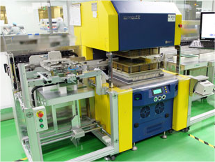
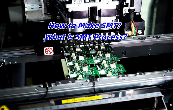
In this stage, pick-and-place machines accurately position components on the PCB. The machines use vacuum or gripper nozzles to remove each component from its packaging and place it onto the board. These machines are fast and precise, capable of placing up to 80,000 components per hour.

Precision is key here, as any misplaced components could lead to costly rework once soldered.

4. Reflow Soldering

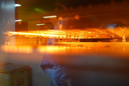
After components are placed, the PCB is moved into the reflow oven for soldering. The board passes through several temperature-controlled zones:

  • Preheat Zone

The temperature is gradually increased to between 140℃ and 160℃ at a rate of 1.0℃-2.0℃ per second to ensure the board and components heat evenly.

  • Soak Zone

The PCB is maintained at this temperature for 60 to 90 seconds to stabilize the heat across the entire board.

  • Reflow Zone

The temperature is then raised to 210℃-230℃ to melt the solder paste, bonding the components to the PCB. The molten solder’s surface tension keeps the components in place during this process.

  • Cooling Zone

In the final zone, the solder is rapidly cooled to solidify the connections and prevent any soldering defects.

For double-sided boards, this process may need to be repeated, either using solder paste or adhesive to secure components.

How to Make SMT? What is SMT Process?

5. Cleaning and Inspection

Once the soldering process is complete, the PCB is cleaned and inspected for any defects. This is done using magnifying lenses, Automated Optical Inspection (AOI), flying probe testers, X-ray inspection, and other tools to ensure accuracy. Any flaws are repaired before the finished product is packaged and stored.

What are the basics of SMT?

SMT simplifies assembly by reducing the need for drilled holes and using smaller components. Unlike traditional through-hole components, SMT parts are placed on the surface of the PCB, making the design more compact.

The basic elements of SMT include:

  • PCBs: The base for components, designed with specific pads for each part.
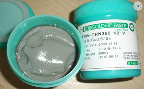
  • Solder Paste: A mixture of metal solder particles and flux, used to create a bond between components and the board.
  • SMT Components: Small electronic parts, such as resistors, capacitors, and ICs, that attach to the PCB.

The transition from through-hole technology to SMT has improved manufacturing speed and performance in electronics.

How do I prepare for SMT?

As the core step of electronic product manufacturing, PCBA’s preparation before assembly directly affects the quality and reliability of the final product. The following is a detailed analysis from multiple dimensions:

1. Component inspection

Before assembly, all electronic components must undergo strict screening and inspection. This includes checking that the component type, package, number of pins, etc. are consistent with the BOM (Bill of Materials), as well as performing the necessary electrical performance tests.

2. Take ESD measures

Static damage to electronic components is invisible, but the consequences are serious. Therefore, when distributing materials and testing IQC, warehouse personnel should wear anti-static gloves, reliably ground the instrument, and lay anti-static rubber MATS on the work surface. During the assembly process, the operator should also wear anti-static clothes, anti-static bracelets and other protective equipment to ensure that the workbench and equipment are well grounded.

3. Cleanliness requirements

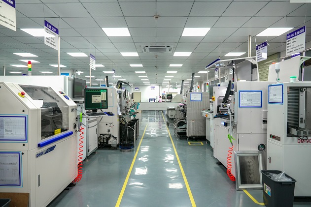
The work workshop and workbench must be kept clean to prevent contaminants such as dust and impurities from entering the circuit board, affecting the accuracy and quality of the patch. Clean the work surface and workshop floor regularly. Smoking, eating and drinking are strictly prohibited in the work area.

How to Make SMT? What is SMT Process?

4. Temperature and humidity control

Appropriate temperature and humidity should be maintained in the workshop to reduce static electricity generation and the impact on electronic components. It is usually recommended that the temperature be controlled at 23Âą3oC and the humidity be controlled at 45% to 70%RH. This environment helps to ensure the quality of welding and the stability of electronic components.

5. PCB appearance check

Before assembly, the PCB board should be visually inspected to confirm whether it is complete, whether the surface coated solder resistance layer is intact, and whether there are obvious short circuits and defects. Use a multimeter to check whether there is a short circuit between the power supply and the ground terminal on the printed board, and ensure that the printed board is fine.

6. Check the software and hardware

When the PCBA needs to be upgraded, the motherboards produced in different time periods should not be mixed together to avoid mixing problems. Before assembly, check whether the final use of the software is in accordance with customer requirements to ensure that the software and hardware are compatible and correct.

7. Welding process selection

According to the layout of the circuit board and the characteristics of the components, select the appropriate welding process (such as wave soldering, reflow welding, hot blast furnace welding, etc.). Each welding method has specific requirements for the placement, orientation and spacing of components that need to be planned in advance.

8. Manually prepare the post-welding plug-in components

For some components that cannot be automatically welded (such as large connectors, heat sinks, etc.), manual plug-in assembly is required. This requires the operator to have a wealth of experience and skilled skills to ensure the accuracy and robustness of the plug-in.

9. Perform ESD operations

During operation, use an ESD workbench and an ESD container to hold components and semi-finished products. All welding equipment should be grounded, the electric soldering iron must be anti-static type, and tested before use.

10 Cleaning and protective treatment

After the assembly is complete, the product needs to be cleaned to remove the residue and contaminants generated during the welding process. At the same time, appropriate protective treatment of the product, such as spraying three anti-paint, etc., to improve the product’s moisture, dust and corrosion resistance.

Which solder paste is used in SMT?

The type of solder paste used in SMT assembly process depends on several factors, such as the materials of the components and the PCB, as well as the operating conditions of the finished product. Generally, there are mainly include high temperature solder paste, ‌ medium temperature solder paste and low temperature solder paste. ‌

  • High temperature solder pastes are commonly used in applications where higher temperatures are required for welding. ‌ has a higher melting point and ‌ is suitable for welding electronic components with specific temperature requirements. ‌
  • Medium temperature solder paste and low temperature solder paste are suitable for medium and low temperature welding respectively, ‌ select the appropriate solder paste type according to the specific welding needs. ‌
How to Make SMT? What is SMT Process?

In addition, ‌ solder paste can also be classified according to the flux activity level, ‌ including “R” (‌ inactive) ‌, ‌ “RMA” class (‌ moderate activity) ‌, ‌ “RA” class (‌ completely reactive) ‌ and “SRA” class ‌ (‌ super activity). ‌ Different types of activity levels are suitable for different application scenarios, ‌ for example, ‌ “R” grade is usually used for welding aerospace, ‌ avionics products, ‌ and “RA” grade is suitable for consumer electronics products. ‌ This classification allows users to choose the right solder paste according to the specific application needs and cleaning process requirements. ‌

What temperature should a soldering iron be for SMT?

The right temperature for soldering in SMT can vary depending on the solder paste and components you’re using. Typically, the soldering iron should be set between 250°C and 300°C. Using a lower temperature might not properly melt the solder, while a higher temperature could damage components or the PCB.

Of course, different types of PCB requires different temperature. For example, ceramic PCBs has fragile surface, so a lower temperature is good.

What are the disadvantages of SMT?

  • Small volume (due to the limitation of components)
  • Fragility
  • High soldering requirements
  • Easily damaged or dropped
  • Challenging to inspect
  • Complex process and inspection
  • High equipment investment

How to solder SMT at home?

Soldering SMT components at home can be tricky, but with the right tools and techniques, it’s doable. Here’s a quick guide:

  1. Tools: You’ll need a fine-tip soldering iron, tweezers, solder paste, and flux. You may also want a magnifying glass or microscope for better visibility.
  2. Apply Solder Paste: Use a small amount of solder paste on the pads of the PCB where you want to place your components.
  3. Place Components: With tweezers, carefully place the components onto the solder paste. Make sure they are properly aligned with the pads.
  4. Reflow the Solder: If you have a reflow oven, you can use it to heat the board. Alternatively, a hot air rework station can also work.
  5. Inspect: Once the solder has cooled, check the connections. If necessary, reheat or add more solder to fix any weak joints.

Best Technology is a one-stop PCB & PCB assembly manufacturer founded in 2006, with 5 assembly lines. If you have needs for PCB and PCBA fabrication, we can be your reliable supplier from prototypes to bulk production. In addition, we have SMT factory in Vietnam, if you don’t want to make smt in Shenzhen, then we can support you in Vietnam. Welcome to contact us if you have such PCB and PCBA projects.

You may also like

What is Tda7294 amplifier board &tda7294 datasheet
Wednesday, August 7th, 2024

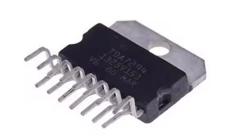
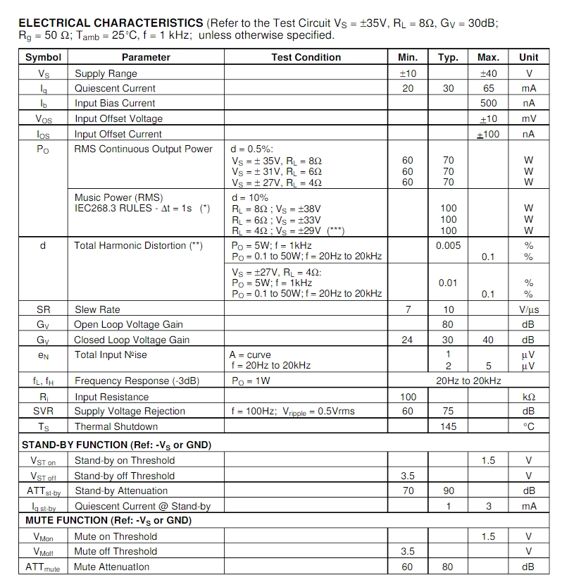
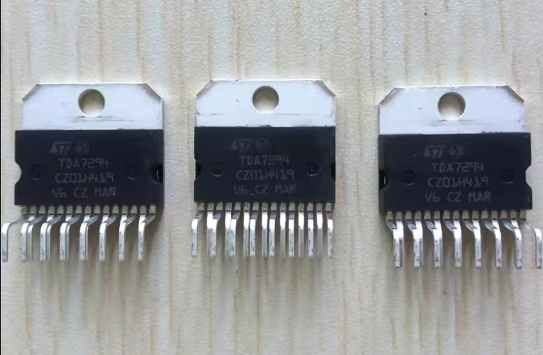
TDA7294 is a class AB monolithic audio amplifier integrated circuit launched by SGS-THOMSON Microelectronics in the 1990s. It swept away the raw, cold and hard sound of previous linear integrated amplifiers and thick film integrated amplifiers, and is widely used in HiFi fields, such as home theaters, active speakers, high-performance TVs and other fields.

The chip adopts a 15-pin dual-row asymmetric plug-in package, the differential input stage is composed of bipolar transistors, and the driver stage and power output stage use DMOS field-effect transistor semiconductor technology. This hybrid semiconductor manufacturing process allows TDA7294 to take into account the advantages of bipolar signal processing circuits and MOS power tubes, and the playback sound is very friendly (it is praised by audiophiles as a “tube-flavored amplifier”); the built-in silent standby function, short-circuit current and overheating protection functions make its performance more perfect. It can be used in HiFi home audio, active audio, high-performance TVs and other fields.

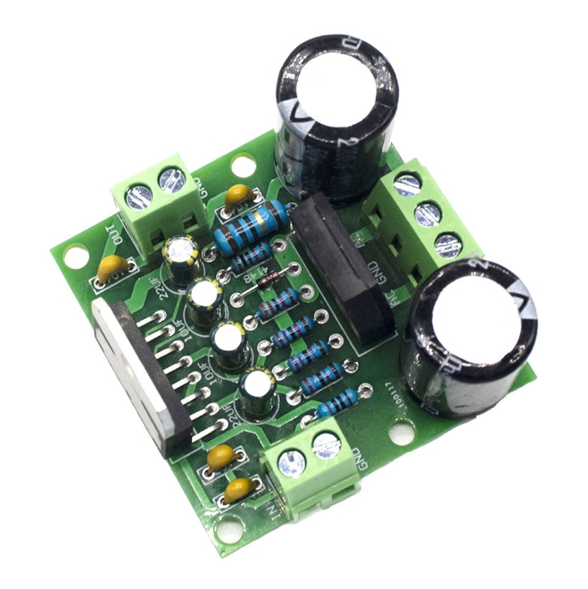
Tda7294 amplifier board

tda7294 amplifier board

tda7294 amplifier board PCBA

  1. This circuit is an official standard circuit, stable and reliable.
  2. The filter uses a large electrolytic capacitor with a withstand voltage of 50V and a capacity of 2200uf.
  3. Power supply voltage: dual 12-36V ring transformer, dual 32V ring transformer is recommended
  4. Output power: 85W*1 undistorted rated power, peak power 100W
  5. Can easily drive speakers above 100W, speaker impedance: 4-8 ohms
  6. PCB size: 50*50mm
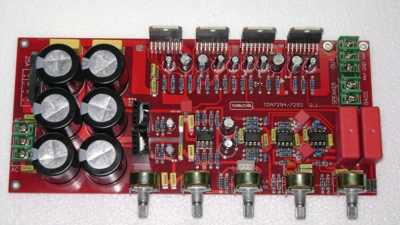
tda7294 amplifier board

Basic parameters:
Power supply: dual 18-28V AC
Power: 2X80W+160W subwoofer
Circuit board size: 218x98MM
Potentiometer function: low frequency frequency adjustment, subwoofer volume. Left and right channel volume, treble, bass.

Adopting the new laser dark word TDA7294
The power filter uses 6 63V3300UF capacitors, and the rectifier uses a 25A imported rectifier flat bridge.
PCB uses 1.6mm thick double-sided board, 2.0 ounces copper thickness, and full tin spraying process to ensure good passing performance of large and small currents.
Fever component assembly, the subwoofer part consists of two new TDA7294 BTL output,
The low-pass filter is designed according to the frequency adjustable design of home theater style (50-150HZ), with strong power!
The left and right channels are served by two TDA7294 respectively, and the input coupling capacitor uses the German imported WIMA 2.2UF coupling capacitor, which makes the sound sweeter!
The signal-to-noise ratio of the board is also very high, and even if you put your ear close to the speaker, you can’t hear the AC noise! ​​It is the best choice for upgrading 2.1 amplifiers!

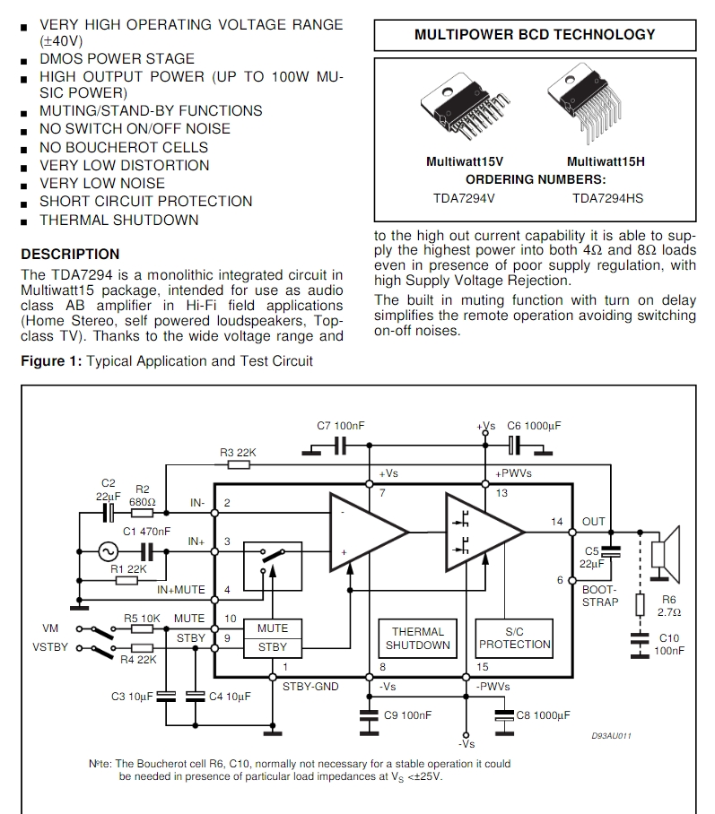
TDA7294 datasheet

TDA7294 datasheet
TDA7294 datasheet

TDA7294 Main Features

Wide supply voltage range: Âą10V ~Âą40V
High output power: 70W (up to 100W)
Standby and mute functions
Noiseless ON/OFF switch
Low noise and low distortion
Short circuit protection and overheat protection

TDA7294

Pin function
Pin 1 is the standby terminal;
Pin 2 is the inverting input terminal;
Pin 3 is the positive input terminal;
Pin 4 is grounded;
Pins 5, 11, and 12 are empty pins;
Pin 6 is the bootstrap terminal;
Pin 7 is +Vs (signal processing part);
Pin 8 is -Vs (signal processing part);
Pin 9 is the standby pin;
Pin 10 is the mute pin;
Pin 13 is +Vs (final stage);
Pin 14 is the output terminal;
Pin 15 is -Vs (final stage)

DIY Production

1) The first step is to get the PCB. Here you can make the PCB yourself by DIY ironing method. Since the PCB is easy to make, the PCB design is kept single layer only, or you can get ready-made quality PCB from best.or custom tda7294 amplifier board.
2) After the PCB is completed, carefully mount all small components like jumpers, resistors, diodes, etc. to the PCB and trim their terminals, then solder them to the PCB first, because there are many components on this board, so it is better to solder them one by one
3) After installing the small components, install the large components like capacitors, fuse holders, rectifiers to the PCB and solder them. (Don’t install the power filter capacitor, 22000uF capacitor for now. Completed in the following steps)
4) After that, it’s time to mount all 7 ICs to the PCB and solder them.
5) Now properly mount the heat sink on the IC using insulating MICA and insulating plastic shoulder washers. Remember to use good quality thermal paste between the heat sink and IC.
6) After mounting the IC on the heat sink. Check the continuity between the heat sink and the IC back plate using a multimeter. There should not be any continuity between them. Please note the heat sink isolation
7) Now mount the cooling fan to the PCB using cable ties or any other suitable method.
The board assembly is now complete. Clean the track side of the board using IPA (Isopropyl Alcohol) or cleaning flux and then power the board using a 20-0-20 VAC transformer or a 24-0-24 VAC transformer.

Which one has better sound quality, TDA7294 or LM3886? Voltage AC 28v

LM3886 has better bass because its maximum current can reach 10A, which means it can drive a 2-ohm box without any problems. From the parameters alone, LM3886 is worse than 7294. And it is true in practice, especially for bass. If the transformer is OK, it feels very powerful. 7294 is not as good as 3886 in bass. The current is large when it comes to bass. 7294 itself has overcurrent protection. When the current reaches a certain level, it starts to limit the output current. However, 7294 is better in treble.

You may also like

How to Make a BOM?
Thursday, July 11th, 2024

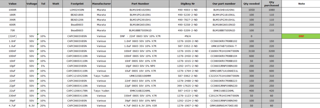
If you are familiar with SMT or PCB assembly process, you may know BOM file. It is an important element in the SMT process. Creating BOM is a crucial step in the manufacturing process, especially for PCBs. A BOM serves as a comprehensive list of all the parts, components, and materials needed to build your product. It ensures that everyone involved in the production process is on the same page, reducing the risk of errors and delays. Today, Best Technology would like to introduce BOM and giving you a guide to create a BOM file step by step.

How to Make a BOM?

What is a Bill of Materials (BOM)?

A Bill of Materials (BOM) is a detailed list of all the parts, components, and materials needed to manufacture a product. In PCB manufacturing, a BOM outlines every item required to assemble a PCB, including quantities, part numbers, and descriptions. It serves as a guide to ensure that the manufacturing process runs smoothly and that no crucial components are missing.

Types of Bill of Materials

There are several types of BOMs used in different stages of production. Each type serves a specific purpose and provides unique details to streamline processes and ensure accuracy. Here are the primary types of BOMs:

  • Engineering BOM

This type of BOM is creating during the design phase. It lists all the parts and components designed by the engineering team, including specifications and relationships as intended in the final product. And of course, it mainly used by design engineers to communicate the product structure and details to manufacturing teams.

  • Manufacturing BOM (Formal)

It is a formal BOM files that used in the assembly phase. Different with engineering BOM, it includes additional details necessary for manufacturing, such as packaging, handling instructions and assembly details. And some special instructions.

  • Sales BOM

Sales BOM is used by sales teams and includes information relevant to the sales process, such as pricing and availability. It helps in providing accurate quotes, managing customer expectations, and handling sales orders efficiently.

What Should Include in an Effective Bill of Materials?

An effective BOM should be detailed, accurate, and easy to understand. It should include all the details of components and indicated revisions. As a 18 years expertise in PCBA production, we summarized the key elements that should be included in the BOM.

  • Component details

It should include all the components and their detailed information, such as names, part numbers (PN), and descriptions for each part.

  • Quantity (QTY)

The exact quantity of each component required for the product. Accurate quantities can prevent shortages and overstocking.

  • Foot print

It is the package of each component, helping to ensure the correction of part.

  • Reference Designators

Unique identifiers that match each component to its specific location on the product layout. These are essential for assembly and troubleshooting.

  • Manufacturer Information

Manufacturer information, including the manufacturer name of components and manufacturer part number. It helps to ensure correct parts are sourced. And convenient for alternative part sourcing if it is shortage.

  • Supplier information (Optional)

It means the name of the supplier or distributor. The part number used by the supplier, which may differ from the manufacturer’s part number.

  • Assembly instructions

Any special notes for assembly such as DNF remark, and version control to track revisions should also be included. Additionally, cost information helps in budgeting, and lifecycle status information helps plan for component availability and avoid discontinued parts.

How to Make a PCB Bill of Materials (BOM)?

Creating a PCB BOM is a systematic process that involves compiling all the necessary information about each component required for the assembly of the PCB. Here’s a detailed guide on how to create a PCB BOM:

  • Open a Blank Spreadsheet

Use software like Microsoft Excel or Google Sheets to start with a blank spreadsheet. They are common to use, offering flexibility and ease of use for creating and managing BOMs.

  • Define Columns

Set up your spreadsheet with appropriate column headers. Common headers include:

  • Part Number
  • Component Name
  • Quantity
  • Reference Designator
  • Manufacturer
  • Manufacturer Part Number
  • Supplier
  • Supplier Part Number
  • Description
  • Package Type
  • Cost
  • Notes
  • Input Data

Enter the required details for each component under the appropriate headers. Please be make sure that all information is accurate and complete. This may involve referencing design files, datasheets, and supplier catalogs. If it is incorrect, then it needs a lot of time to find out and revise the errors, resulting in schedule delay.

  • Use Formulas

Utilize Excel formulas to automate calculations, such as summing total quantities or calculating costs. This helps in reducing manual errors and saves time.

  • Format for Clarity

Use cell formatting options to highlight important information and ensure the spreadsheet is easy to read. For example, you can use bold text for column headers, color coding for different component types, and borders to separate sections.

  • Include Version Control

Add a version control section to your BOM to track revisions and updates. This can be a simple row at the top or bottom of the spreadsheet, indicating the version number, date of revision, and a brief description of changes.

How to Make a BOM?
(BOM file reference)
  • Save and Update

Save your BOM and update it regularly to reflect any changes in the design or component availability. Regular updates ensure that the BOM remains accurate and up-to-date, preventing issues during production.

  • Review and Verify

Have multiple team members review the BOM for accuracy. Cross-check all component details, quantities, and part numbers against the design files. Verification helps catch errors early and ensures the BOM is reliable.

  • Communicate with Suppliers:

Maintain open communication with suppliers to confirm component details and availability. This ensures that you can source the correct parts and avoid delays in the production process.

How Can I Optimize My BOM for PCB Assembly?

Sometimes, a simple BOM is not good to process PCB assembly process, and manufacturers may need to spend a lot of time to optimize it, make into convenient for manufacturing. If you are a layman, here are some steps to help you in optimizing your BOM file.

First, it’s a good idea to standardize components where possible. Using standard parts that are readily available from multiple suppliers can simplify procurement and reduce costs. This approach minimizes the risk of shortages and ensures you can get parts quickly and affordably. Also, make sure all entries in your BOM are clear and concise to avoid confusion during assembly. Double-checking part numbers and quantities against design files is crucial to prevent errors that could lead to rework or delays.

Building strong relationships with your suppliers is another key factor. Good communication with suppliers helps ensure reliable component availability and keeps you informed about any changes in lead times or part availability. Regularly updating your BOM to reflect any design changes or component availability issues is essential. Keeping your BOM current and accurate prevents last-minute surprises during assembly.

How to Make a BOM?

What Common Mistakes Should I Avoid When Creating a PCB BOM?

Avoiding common mistakes in BOM creation can save time and reduce errors. Here are some pitfalls to watch out for:

  • Incomplete information – ensure all necessary details are included for each component.
  • Incorrect quantities – double-check quantities to avoid shortages or excess inventory.
  • Outdated data – keep the BOM updated with the latest design changes and component information.
  • Ambiguous descriptions – provide clear and precise descriptions to prevent confusion.
  • Lack of version information – implement version control to track changes and ensure the correct BOM version is used.

Creating an effective and accurate PCB BOM is essential for smooth manufacturing and assembly. By following best practices and using the right tools, you can ensure your BOM is comprehensive, clear, and up-to-date, ultimately leading to a successful PCB production process.

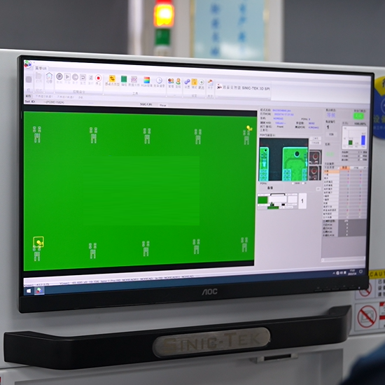
Best Technology is an expert in SMT and PCB assembly, we have more than 18 years in this industry, that can offer you a best experience of PCBA solution. In our facotry, we have advanced equipment like full auto pick and place machine, online dual AOI, X-ray, 3D SPI, nitride reflow oven and three-proof paint machine. So that we can ensure the fast lead time and high quality of your PCBA products. Reach us to get a instant quote!

You may also like

What Are the Differences Between Active and Passive Components?
Wednesday, July 3rd, 2024

In PCB electronics, components are classified into two main categories: active and passive components. Understanding these differences is crucial for anyone working with electronic circuits. Active components control electricity flow and require an external power source. Passive components do not control electricity and do not need an external power source.

What are active and passive components meaning?

Active and passive components, simply say, the device that needs an energy (electrical) source is called an active device, and the device that does not need an energy source is a passive device. Active components, such as transistors and diodes, require external power to function. They can control the flow of electricity. Passive components, like resistors and capacitors, do not need external power. They cannot control electrical flow but can store, resist, or filter energy. Both passive and active components are common useful in PCB assembly and SMT technology.

Active components play a dynamic role in circuits. They can amplify signals, switch currents, and perform various complex functions. These components rely on an external power source to operate and influence the behavior of the circuit. For instance, a transistor can amplify a weak signal, making it stronger and more useful for further processing.

What Are the Differences Between Active and Passive Components?

Passive components, on the other hand, are more static in nature. They cannot amplify signals or control current flow but are essential for other functions like energy storage and signal filtering. Resistors, capacitors, inductors, and transformers are common examples. Each of these components has a specific role in maintaining the stability and functionality of an electronic circuit.

What are the key differences between active and passive components?

The main difference between active and passive components is their ability to control electricity. Active components can amplify signals and perform complex tasks. Passive components can only store, resist, or filter energy. They cannot amplify signals or control current.

Active components are energy-dependent. They require an external source of power to function and can influence the flow of electricity within the circuit. For example, an integrated circuit (IC) can perform multiple functions like amplification, switching, and signal modulation, all of which require external power.

Passive components, in contrast, do not require an external power source. They can only perform their functions passively. For instance, a resistor can limit the current flowing through a circuit without needing additional power. Similarly, a capacitor can store electrical energy and release it when needed, all without external energy input.

Common active components in electronics

Active devices are the main components of electronic circuits. From the physical structure, circuit function and engineering parameters, active devices can be divided into discrete devices and integrated circuits.

1. Discrete devices

  • Bipolar transistor, generally referred to as transistor or BJT
  • Field effective transistor
  • Thyristor
  • Semiconductor resistors and capacitors – resistors and capacitors manufactured by integrated technology are used in integrated circuits.

2. Integrated circuit

Integrated circuit can be divided into analog IC and digital IC. Analog integrated circuits mainly deal with continuous analog signals, such as sound, light, temperature, etc., and retain the continuity and accuracy of the signal through amplification, filtering, mixing and other operations. In contrast, digital integrated circuits are used to process discrete time digital signals, convert the signal into binary digital form, and then perform logical operations and processing.

Basic analog integrated circuit devices generally include:

  • Integrated operational amplifier (operation amplifier)
  • Comparator
  • Logarithmic and exponential amplifiers
  • Multiplier/divider
  • Analog switching circuit (analog switch)
  • Phase lock loop
  • Integrated voltage regulator
  • Reference source
  • Wave-form generator
  • Power amplifier

Digital integrated circuit including:

  • Logic gate circuit
  • Flip-flop
  • Register
  • Decoder
  • Data comparator
  • Driver
  • Counter
  • Shaping circuit
  • Programmable Logic Device (PLD)
  • Microprocessor (MPU)
  • Microcontroller (MCU)
  • Digital signal processor (DSP)

Common passive components in electronics

Passive devices in electronic systems can be divided into circuit components and connection components according to the circuit functions they play. These components are essential for functions like energy storage, filtering, and impedance matching in electronic circuits. The common passive components are including:

Circuit components

  1. Diode
  2. Resistor
  3. Resistor network
  4. Capacitor
  5. Inductor
  6. Transformer
  7. Relay
  8. Key
  9. Speaker
  10. Switch

Connection components

  • Connector
  • Socket
  • Cable
  • PCB (printed circuit board)

Why are active components crucial in modern electronics?

The ability of active components to control and manipulate electrical signals makes them indispensable in a wide range of applications.

In computers, for example, active components such as processors and memory chips perform complex calculations and store large amounts of data. In communication systems, active components amplify weak signals, making long-distance transmission possible. Without these amplifiers, the signal would decay with distance, leading to a decline in communication quality. Power electronics, another key area of modern development, relies heavily on active components. Devices like power converters, inverters, and motor controllers use transistors and integrated circuits to efficiently convert and control electrical energy. This efficiency is crucial for applications ranging from renewable energy systems to electric vehicles.

It’s fair to say that without active components, devices like computers, smartphones, and TVS wouldn’t function the way they do today, and our era of big data wouldn’t be moving as fast as it is today.

How do passive components complement active components?

Both active and passive components are indispensable in a circuit. They depend on each other and complement each other. Without active components, the circuit cannot be activated or perform a specific work. Without passive components, the circuit cannot be controlled and adjusted, nor can it achieve a stable operating state. Such a relationship between the two is like the relationship between the “dynamic” and the “static” of a circuit.

What Are the Differences Between Active and Passive Components?

For example, in an audio amplifier circuit, the power supply and amplifier are the active components, and the load and resistance are the passive components. The power supply provides energy, the amplifier amplifies the signal, and controls and limits it through load and resistance, and finally realizes the amplification and regulation of the audio signal. In signal processing, inductors filter out high-frequency noise and protect sensitive active components from interference. Transformers, on the other hand, enable efficient power transfer between different parts of the circuit, allowing active components to operate within their optimal voltage range.

Comparing the Energy Requirements of Active and Passive Elements

Active components need an external power source to function. They consume energy during operation. Passive components do not need external power and generally do not consume energy, except for minor resistive losses. This difference impacts the design and efficiency of electronic circuits.

Active components, such as transistors and integrated circuits, rely on external power to operate. This power requirement means that active components consume energy during their operation. The amount of energy consumed depends on the specific component and its application. For instance, a power amplifier consumes more energy than a simple transistor switch.

Passive components, in contrast, do not need external power to function. They operate solely based on the electrical energy present in the circuit. Resistors, capacitors, and inductors do not consume significant energy, except for minor resistive losses in resistors. This low energy requirement makes passive components more efficient in certain applications.

What Are the Differences Between Active and Passive Components?

The difference in energy requirements between active and passive components impacts the overall efficiency of electronic circuits. Designers must carefully balance the use of active and passive components to achieve optimal performance and energy efficiency. For example, using passive filters instead of active ones can save energy in low-power applications.

Active and Passive Component Images and Symbols

Recognizing symbols are essential for reading and designing circuit diagrams. They provide a visual representation of the components and their functions, helping designers understand the overall structure and operation of the circuit. Recognizing these symbols is a fundamental skill for anyone involved in electronics. Here is a detailed images and symbols listing of common active and passive components.

Above all is the introduction to passive and active components, hope it is useful for every engineers. Best Technology is a professional PCB and PCBA manufacturer in Asia. We have our own factory in China and Vetnam. Welcome to contact us if you have any questions about components and PCB assembly.

You may also like

Why Solder Paste became Dry and How to Solve This Problem
Thursday, August 18th, 2022

As a One-stop PCBA manufacturer, I believe most of manufacturers have faced a problem of solder paste became dry during SMT process, especially in hot summer, and there will be a large number of defects come out when solder paste was dry, such as poor printing, false solder, components be shifted, cold solder and so on, which will greatly decrease assembly efficiency and PCBA quality.

Do you know why the solder paste became dry?

A serious dried solder paste
Good solder paste

After checking and discussing with our SMT engineers, we found the root cause of solder paste be dry is corrosion, in below images you can see the detailed solder powder morphology of corrosion.

2-a Solder powder from good solder paste
2-b Solder powder from dried solder paste

In generally, the main reason of corrosion is thermodynamic instability of metal, that is metal and its alloy is in a high free energy status than other chemical compound (for example, oxide, hydroxide, salt or others), when this situation occurs, metal will transform to lower energy, which is called corrosion.

Metal corrosion is under the basis of the theory of electrochemical, and it’s required four main elements: anode, cathode, electrolyte and constitute current path.

Now let’s parse the mainly metals in solder paste — Sn, Ag, Cu (or other impurities), then under the action of flux medium, numerous galvanic cells with Sn as the cathode and Ag/Cu as the anode are formed, then below chemical reaction will be happened:

Cathode: Sn – 2e → Sn2+

Anode: O2 + H2O + 4e → 4OH

That is: Sn + H2O + ½O2 â†’ Sn(OH)2

Sn(OH)2 decompose: Sn(OH)2 → SnO + H2O

Then chemical reaction of corrosion of solder powder under the moisture in the air can be described as:

The following figure shows the infrared spectrum of succinic acid liquor before and after soaking the solder powder. It can be clearly seen that the soaked liquor contains carboxyl. Therefore, in the solder paste system, except the oxidation reaction of electrochemical corrosion, salinization chemical reaction will be happened too:

Infrared spectrum of Chemical reaction between succinic acid solution and solder powder succinic acid liquor

So now, do you know why solder paste will be dry? And why it is more seriously in hot summer with high temperature and humidity?

Yes, its root cause is not only high temperature in summer, also the humidity is so high (humidity is 70-85% in the summer of Shenzhen City), flux and solder powder will increase the adsorption of water molecules, and due to water is electrolyte of the galvanic cell reaction, it will aggravate the hydrolysis of flux, stimulate the activity of flux, then finally the reaction on the surface of the solder powder is aggravating, and the vicious cycle eventually changes the physical properties of the solder paste.

Then how to solve this problem?

  1. Warm up solder paste before using

Generally, in order to slow down the reaction of flux and solder powder, as well as extend the storage period, the solder paste needed to be stored in a refrigerator with 2-10oC degree. So before using, it is better to take out solder paste and put in standard room temperature for warming up first. A can of 500g solder paste need to be rewarmed at least 2 hours, to make sure its temperature is the same as rooms’. (Normally that period of warming up time is 4 hours in Best Technology.) Otherwise, insufficient warming up will cause the water vapor in the air to condense and enter the solder paste due to the temperature difference, and result in solder paste be dry finally.

  • Environment temperature and humidity

The best storage temp of solder paste is 2-10oC, but the recommended working environment temp is 20-25oC, relative humidity is 30%-60%. (There’re additional humidifiers in the workshop of Best Technology, to make sure suitable humidity in the dry season such as Winter and Spring, and of course the air conditioner in Summer time to decrease the humidity) Usually, the rate of chemical reaction will approximately double, as the temperature increases by 10℃, so the high temperature will increase the volatilization of the solvent in the solder paste and the reaction speed of flux with powder, so the solder paste is easily to be dry. Meanwhile, low temperature will affect the viscosity and expansion of solder paste, and then will cause the poor soldering. At the same time, high humidity will also greatly increase the water vapor entering the solder paste; However, low humidity also affects the volatilization rate of solvent in solder paste.

  • For those solder paste that became dried already, it is better to dilute with flux provided by manufacturer of solder paste.

In a word, when use and store solder paste, we should pay more attention to its temperature & humidity, to make sure high quality of SMT can be achieved. Pls contact Best Technology if you have any questions or comments on solder paste, or SMT.

You may also like

X-ray Inspection in PCB Assembly
Wednesday, June 15th, 2022

X-Ray Inspection’s Definition

X-ray inspection is a technology used to inspect the hidden features of the target objects or products. As for PCB inspection, X-ray is commonly used in the inspection of PCB assembly in order to test the quality and find the hidden defects, X-ray inspection is one of the most important steps for quality-oriented PCB manufacturers.

X-Ray Machine

X-Ray Inspection’s Working Principle

Generally, there are three elements in the X-ray devices.

  • X-ray tube—to generate the X-ray photons.
  • Operation platform—to move along with the sample so that the sample can be inspected from different angles and magnification.
  • Detector—it can capture the X-ray through the samples and then transfer it into the image so that we can find out whether there are defects on the printed circuit board.

The Hidden Defects that can be Identified by X-Ray

Since PCB has the higher density with the solder joints hidden and holes buried or blind, X-ray enable us to inspect the quality of the PCB and identify various hidden defects. And there are three common hidden defects that can be inspected by X-ray.

PCB’s Image Under X-Ray
  • Solder bridges—it is a common issue that will occur when the solder joints are so close that they create a connection which is not allowed. And usually, the solder bridges will be covered by some components on the PCB. But they can be easily found with the help of the X-ray device.
  • Solder voids—when gas or flux is entrained during welding, solder voids will be produced, which will lower the thermal conductivity at the solder joint and may cause physical defects. And X-ray can help to  identify the solder voids
  • Pin-hole fills—pin-hole fills issue is a common problem occurring in the plug-in components on the  printed circuit boards. The X-ray device can be used to identify these errors, and can even quantify the missing filling amount.

Our X-Ray Inspection Device

The maximum size of the board that can be put in the device’s operation platform is 510*430 mm, while the maximum inspection size of the device is 435*385 mm. So here is the manifestation of the operation platform’s function. When the size of PCB is over 435*385 mm, the operation platform will move along with the board so that the board can be inspected thoroughly.

And here is a video about operation of our X-ray inspection device.

So, this is the end of this article. In case if you have any questions, you are welcome to contact us via email at  sales@bestpcbs.com. We are fully equipped to handle your PCB  manufacturing requirements.

You may also like

The Basics of Printed Circuit Board Assembly(SMT)
Friday, November 1st, 2019

Printed circuit board assembly(SMT), also known as “stuffing” or “populating” the bare printed circuit board, is quite an intricate process which involves many different stages.  Best Technology’ in house printed circuit board assembly service makes ordering your turnkey printed circuit boards a hassle-free experience as you can count on the industry’s largest support team to help you control every step of the process.

Here are some of the basic elements involved in the printed circuit board assembly process:

Solder Paste Ă˘â‚Źâ€œ Solder paste is a combination of flux, a chemical created to assist in the bonding and melting of the metal, and small fragments of metal (solder) so as to apply the electronic components to the printed circuit board. The paste is placed on the board in specific places along the board in exact amounts with the use of a Solder Stencil and a paste application machine, automatically.

Pick and Place Machine – This machine is essential in an automated printed circuit board assembly process.  The machine is programmed to automatically coordinate with complete accuracy the places to precisely mount each electronic component to be soldered to the printed circuit board. These machines are exact and quick.

Infrared Reflow Ă˘â‚Źâ€œ After the precise bonding element (solder paste) is applied to the PCB, the board will be directed to the reflow oven to join the electronic components to the board by melting the solder paste. This “oven” is comprised of many heaters whose main function is to heat the board to a precise temperature and control the level of cooldown as the solder hardens. This process is crucial to the creation of properly functioning electronics. The printed circuit board will run through a series of testing to ensure no issues or short-circuiting nor misalignments have occurred.

You may also like