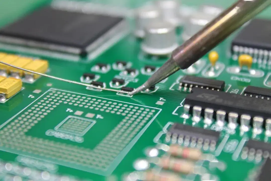
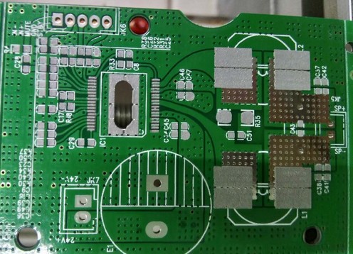
In PCB electronics, components are classified into two main categories: active and passive components. Understanding these differences is crucial for anyone working with electronic circuits. Active components control electricity flow and require an external power source. Passive components do not control electricity and do not need an external power source.
What are active and passive components meaning?
Active and passive components, simply say, the device that needs an energy (electrical) source is called an active device, and the device that does not need an energy source is a passive device. Active components, such as transistors and diodes, require external power to function. They can control the flow of electricity. Passive components, like resistors and capacitors, do not need external power. They cannot control electrical flow but can store, resist, or filter energy. Both passive and active components are common useful in PCB assembly and SMT technology.
Active components play a dynamic role in circuits. They can amplify signals, switch currents, and perform various complex functions. These components rely on an external power source to operate and influence the behavior of the circuit. For instance, a transistor can amplify a weak signal, making it stronger and more useful for further processing.
Passive components, on the other hand, are more static in nature. They cannot amplify signals or control current flow but are essential for other functions like energy storage and signal filtering. Resistors, capacitors, inductors, and transformers are common examples. Each of these components has a specific role in maintaining the stability and functionality of an electronic circuit.
What are the key differences between active and passive components?
The main difference between active and passive components is their ability to control electricity. Active components can amplify signals and perform complex tasks. Passive components can only store, resist, or filter energy. They cannot amplify signals or control current.
Active components are energy-dependent. They require an external source of power to function and can influence the flow of electricity within the circuit. For example, an integrated circuit (IC) can perform multiple functions like amplification, switching, and signal modulation, all of which require external power.
Passive components, in contrast, do not require an external power source. They can only perform their functions passively. For instance, a resistor can limit the current flowing through a circuit without needing additional power. Similarly, a capacitor can store electrical energy and release it when needed, all without external energy input.
Common active components in electronics
Active devices are the main components of electronic circuits. From the physical structure, circuit function and engineering parameters, active devices can be divided into discrete devices and integrated circuits.
1. Discrete devices
- Bipolar transistor, generally referred to as transistor or BJT
- Field effective transistor
- Thyristor
- Semiconductor resistors and capacitors – resistors and capacitors manufactured by integrated technology are used in integrated circuits.
2. Integrated circuit
Integrated circuit can be divided into analog IC and digital IC. Analog integrated circuits mainly deal with continuous analog signals, such as sound, light, temperature, etc., and retain the continuity and accuracy of the signal through amplification, filtering, mixing and other operations. In contrast, digital integrated circuits are used to process discrete time digital signals, convert the signal into binary digital form, and then perform logical operations and processing.
Basic analog integrated circuit devices generally include:
- Integrated operational amplifier (operation amplifier)
- Comparator
- Logarithmic and exponential amplifiers
- Multiplier/divider
- Analog switching circuit (analog switch)
- Phase lock loop
- Integrated voltage regulator
- Reference source
- Wave-form generator
- Power amplifier
Digital integrated circuit including:
- Logic gate circuit
- Flip-flop
- Register
- Decoder
- Data comparator
- Driver
- Counter
- Shaping circuit
- Programmable Logic Device (PLD)
- Microprocessor (MPU)
- Microcontroller (MCU)
- Digital signal processor (DSP)
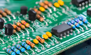
Common passive components in electronics
Passive devices in electronic systems can be divided into circuit components and connection components according to the circuit functions they play. These components are essential for functions like energy storage, filtering, and impedance matching in electronic circuits. The common passive components are including:
Circuit components
- Diode
- Resistor
- Resistor network
- Capacitor
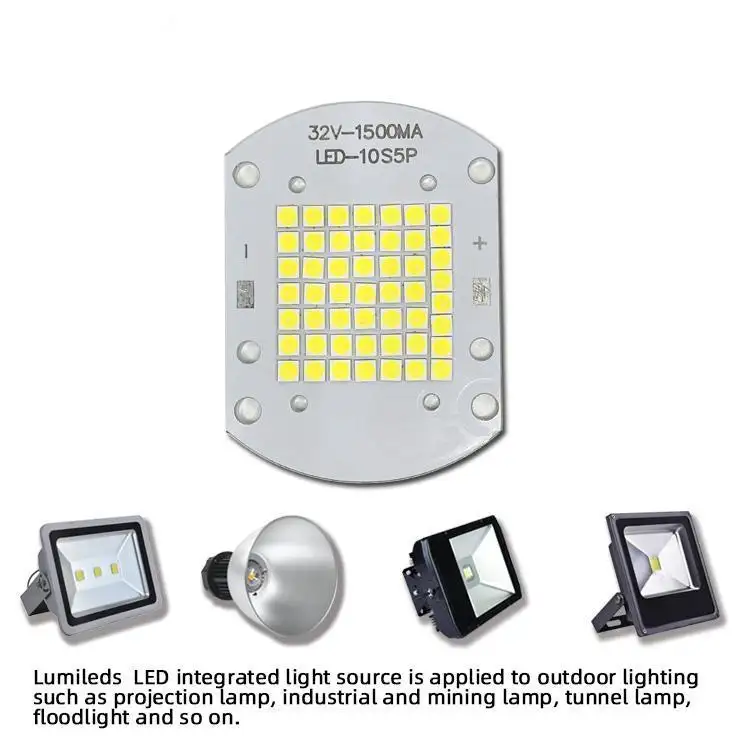
- Inductor
- Transformer
- Relay
- Key
- Speaker
- Switch
Connection components
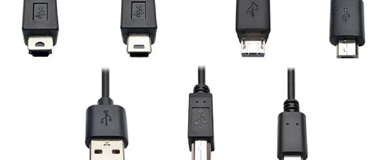
- Connector
- Socket
- Cable
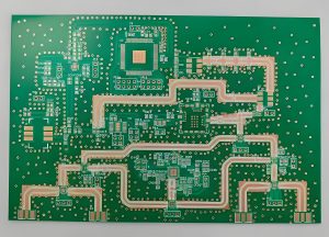
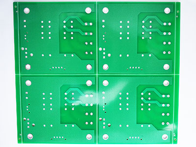
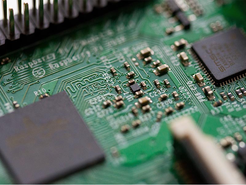
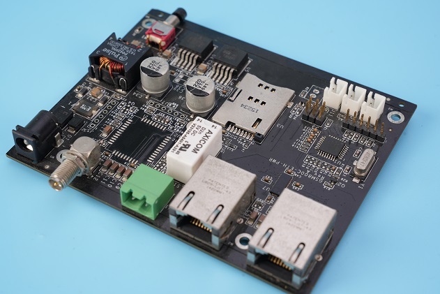
- PCB (printed circuit board)
Why are active components crucial in modern electronics?
The ability of active components to control and manipulate electrical signals makes them indispensable in a wide range of applications.
In computers, for example, active components such as processors and memory chips perform complex calculations and store large amounts of data. In communication systems, active components amplify weak signals, making long-distance transmission possible. Without these amplifiers, the signal would decay with distance, leading to a decline in communication quality. Power electronics, another key area of modern development, relies heavily on active components. Devices like power converters, inverters, and motor controllers use transistors and integrated circuits to efficiently convert and control electrical energy. This efficiency is crucial for applications ranging from renewable energy systems to electric vehicles.
It’s fair to say that without active components, devices like computers, smartphones, and TVS wouldn’t function the way they do today, and our era of big data wouldn’t be moving as fast as it is today.
How do passive components complement active components?
Both active and passive components are indispensable in a circuit. They depend on each other and complement each other. Without active components, the circuit cannot be activated or perform a specific work. Without passive components, the circuit cannot be controlled and adjusted, nor can it achieve a stable operating state. Such a relationship between the two is like the relationship between the “dynamic” and the “static” of a circuit.
For example, in an audio amplifier circuit, the power supply and amplifier are the active components, and the load and resistance are the passive components. The power supply provides energy, the amplifier amplifies the signal, and controls and limits it through load and resistance, and finally realizes the amplification and regulation of the audio signal. In signal processing, inductors filter out high-frequency noise and protect sensitive active components from interference. Transformers, on the other hand, enable efficient power transfer between different parts of the circuit, allowing active components to operate within their optimal voltage range.
Comparing the Energy Requirements of Active and Passive Elements
Active components need an external power source to function. They consume energy during operation. Passive components do not need external power and generally do not consume energy, except for minor resistive losses. This difference impacts the design and efficiency of electronic circuits.
Active components, such as transistors and integrated circuits, rely on external power to operate. This power requirement means that active components consume energy during their operation. The amount of energy consumed depends on the specific component and its application. For instance, a power amplifier consumes more energy than a simple transistor switch.
Passive components, in contrast, do not need external power to function. They operate solely based on the electrical energy present in the circuit. Resistors, capacitors, and inductors do not consume significant energy, except for minor resistive losses in resistors. This low energy requirement makes passive components more efficient in certain applications.

The difference in energy requirements between active and passive components impacts the overall efficiency of electronic circuits. Designers must carefully balance the use of active and passive components to achieve optimal performance and energy efficiency. For example, using passive filters instead of active ones can save energy in low-power applications.
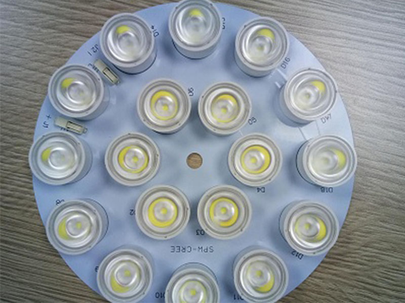
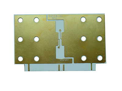
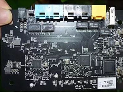
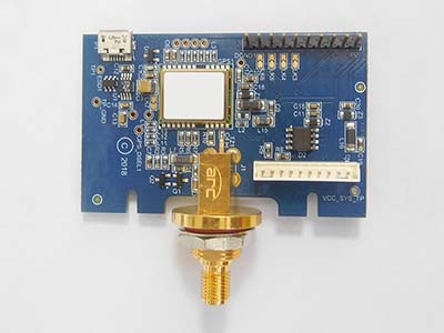
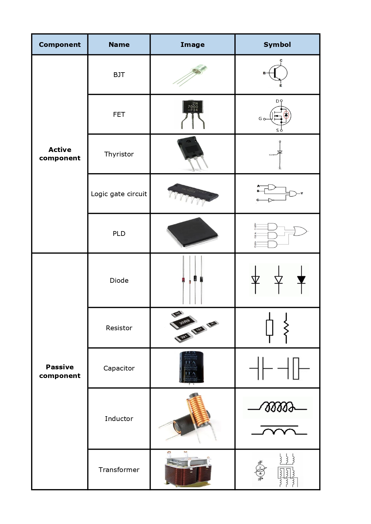
Active and Passive Component Images and Symbols
Recognizing symbols are essential for reading and designing circuit diagrams. They provide a visual representation of the components and their functions, helping designers understand the overall structure and operation of the circuit. Recognizing these symbols is a fundamental skill for anyone involved in electronics. Here is a detailed images and symbols listing of common active and passive components.
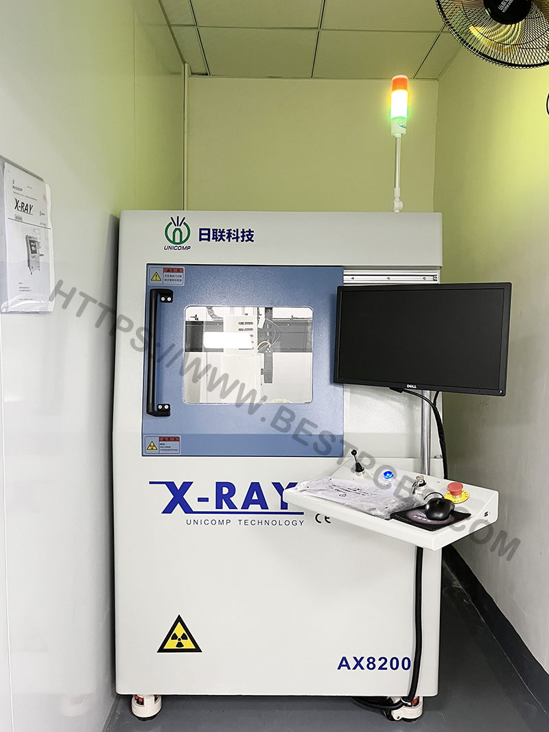
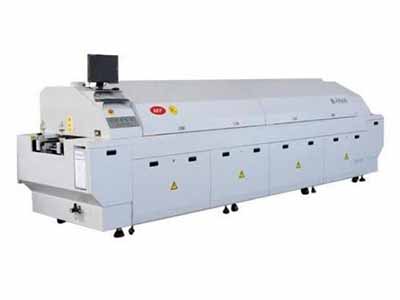
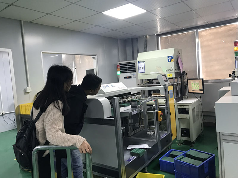
Above all is the introduction to passive and active components, hope it is useful for every engineers. EBest Circuit (Best Technology) is a professional PCB and PCBA manufacturer in Asia. We have our own factory in China and Vetnam. Welcome to contact us if you have any questions about components and PCB assembly.