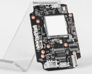
PCB assembly involves mounting electronic components onto bare PCB boards to create semi-finished devices. In this process, soldering is the initial and essential step. Today, we’ll discuss the common soldering issues that arise during PCB assembly and how to prevent them.
Soldering Defects
Soldering defects are issues that arise when joints do not meet the expected quality standards. These defects can impact the functionality, reliability, and longevity of a product.
Some typical issues include software design flaws, overheating, incorrect component placement, and power supply issues. Every manufacturer should be aware of these potential pitfalls to ensure reliable and efficient PCB assembly.
Why Soldering Defects Occur?
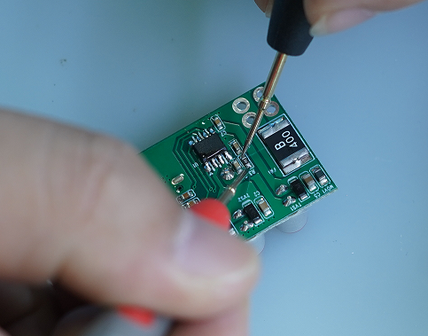
Soldering defects can occur during the assembly process, potentially leading to wasted resources, damaged reputation, product malfunctions, and most critically, loss of time—frustrating both manufacturers and clients. However, by understanding common PCB failure causes, you can address them quickly and effectively.
Poor Solderability of Holes Vias
Poor solderability of holes can lead to soldering defects, affecting the parameters of components in the circuit and causing unstable connections between components and inner layers in multilayer boards. This can result in the failure of the entire circuit.
Soldering Temperature
The soldering temperature, whether too high or too low, and inadequate surface cleanliness can affect the soldering quality. When the temperature is too high, the solder spreads quickly and is prone to oxidation, leading to defects. When the temperature is too low, the solder may not fully melt, resulting in weak joints.
Flux Issues
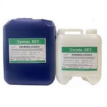
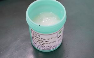
The quality and application of flux also impact soldering quality. Insufficient or poor-quality flux can cause poor wetting, resulting in weak and dull solder joints. Excessive flux may lead to overheating, causing rough joint surfaces.
Solder Issues
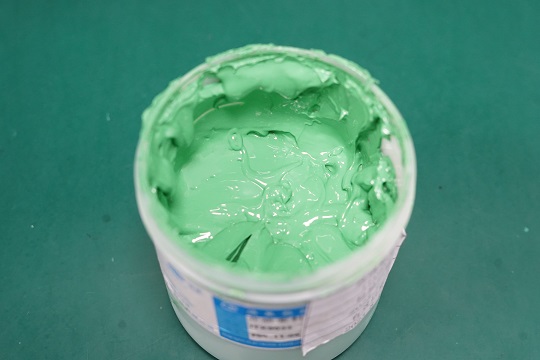
The quality and fluidity of the solder directly affect the soldering outcome. Poor-quality solder or solder with low fluidity can lead to weak and dull joints, or defects where the solder covers less than 80% of the pad.
PCB Design Issues
Poor PCB design can also result in soldering defects. For example, excessively long traces can increase impedance and noise, affecting soldering quality. Components generating heat without proper heat dissipation can also lead to soldering issues.
Operational Issues During Soldering
Problems such as insufficient soldering time, improper temperature control, or loose component leads during soldering can all result in defects.
How many types of soldering defects are there?
There are several types of soldering defects that can occur during the PCB assembly process. Here is a list of common soldering defects:
- Cold Joints
- Bridging
- Insufficient Solder
- Solder Balls
- Voids
- Cracked Joints
- Non-wetting
- Tombstoning
- Pin Holes or Blow Holes
- Oxidation Defects
- De-wetting
- Component Misalignment
- Solder Splashes
- Excessive Solder
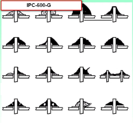
How Do You Troubleshoot Soldering? -One by One
- Cold Joints
Cold joints occur when the solder doesn’t heat properly, resulting in weak, dull, and rough connections. To prevent this, use a soldering iron with adequate power and maintain the correct soldering temperature (typically between 350°C to 400°C for leaded solder). Ensure that both the pad and component lead are evenly heated before applying solder. The solder should flow smoothly around the joint. Using a clean, well-tinned soldering iron tip ensures efficient heat transfer. Additionally, avoid moving the joint before the solder has fully solidified.
- Bridging
Bridging happens when excess solder connects adjacent leads, creating shorts. To avoid this, apply an appropriate amount of solder paste using a stencil with the right thickness. Use a fine-tipped soldering iron or a hot air rework tool to apply heat precisely. If bridging occurs, use a desoldering braid or a vacuum desoldering tool to remove excess solder. Practice steady hand movements when applying solder manually and avoid dragging the soldering tip across pads.
- Insufficient Solder
Insufficient solder leads to weak joints that can easily break. To fix this, ensure that enough solder paste is applied during the assembly process. Check that the soldering tip transfers enough heat to allow solder to flow adequately across the pad and component lead. If needed, reflow the joint by reheating and adding a small amount of solder to improve coverage and strength.
- Solder Balls
Solder balls are tiny spherical particles that can detach and create shorts. To prevent this, maintain a proper reflow profile that allows gradual heating and cooling. Ensure that the solder paste is of high quality and free from contamination. Clean the PCB surface thoroughly to remove dust and oil. Control the application of solder paste to prevent excessive paste that could splatter during heating.
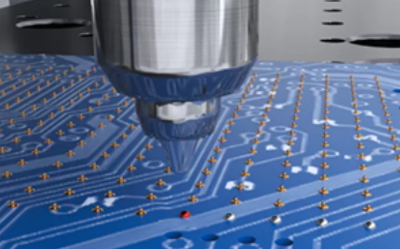
- Voids
Voids are gaps in the solder joint caused by trapped gas or flux residue. To minimize voids, pre-bake PCBs to remove moisture that can turn into steam during soldering. Use high-quality, low-residue flux and ensure even application. Adjust the reflow profile to give enough time for gases to escape before the solder solidifies. This reduces the chances of void formation.
- Cracked Joints
Cracked joints can form due to rapid cooling or mechanical stress. Allow the solder joint to cool naturally without sudden air exposure. Ensure the PCB is not moved or subjected to vibrations while the solder is cooling. Choose solder materials with good thermal expansion properties to withstand temperature changes. For wave soldering, ensure that components are secure on the PCB before the process starts.
- Non-wetting
Non-wetting occurs when the solder does not adhere properly to the pad or lead. This issue is often due to surface contamination or oxidation. Clean the board thoroughly with isopropyl alcohol or a PCB cleaner to remove oils, oxidation, or other contaminants. Use high-quality flux that promotes wetting and re-tin oxidized component leads before soldering. Ensure that the soldering temperature is within the recommended range for proper flow and adhesion.
- Tombstoning
Tombstoning happens when one side of a component lifts off the PCB due to uneven heating. This can be addressed by ensuring an even reflow profile where both sides of the component are heated simultaneously. Verify that the solder paste deposit is balanced on each pad to prevent uneven solder melting. Additionally, using smaller components with balanced thermal mass can help prevent tombstoning.
- Pin Holes or Blow Holes
Solution: Pin holes or blow holes result from gas escaping during soldering. To reduce this, pre-bake PCBs at a low temperature (e.g., 100°C for one hour) to remove moisture. Use flux that contains fewer volatile components. Optimize the reflow profile to allow flux and trapped gases to escape before the solder solidifies. Ensure that the soldering environment has low humidity to further minimize gas formation.
- Oxidation Defects
Oxidation occurs when solder joints are exposed to air for too long before the soldering process. To prevent oxidation, apply flux shortly before soldering to create a barrier against air. Use a nitrogen atmosphere in reflow ovens to reduce oxidation. Regularly clean the soldering tip and apply fresh solder to prevent oxidation on the tip itself.
- De-wetting
De-wetting occurs when the solder initially wets the pad but retracts, leaving an uneven surface. This can be caused by contamination or poor-quality solder. Ensure the soldering surface is free from contaminants and oxides by cleaning it with an appropriate cleaner. Use high-quality solder and maintain an optimal soldering temperature to allow proper wetting without over-stressing the solder.
- Component Misalignment
Misaligned components can lead to poor connections and defects. Use automated pick-and-place machines for accurate component positioning. Check component alignment manually before reflow if placing by hand. During reflow, use alignment aids or fixtures to ensure components stay in place. Verify that the solder paste stencil and reflow settings are precise for even solder distribution.
- Solder Splashes
Solder splashes are small splatters of solder that can lead to shorts or contamination. To prevent this, maintain a consistent reflow profile and avoid sudden movements during the soldering process. Check that solder paste is applied evenly, without excess. Ensure that the soldering environment is stable and free of vibrations.
- Excessive Solder
Excessive solder can create thick joints or bridges between pads. Apply solder paste using a stencil with an appropriate aperture size for precise control. Train operators to apply the right amount of solder during manual soldering. Use a fine-tipped soldering iron for better control and to prevent large, excessive solder deposits.
Best Technology is a professional PCBA manufacturer in Asia, we have a 3000+ working area in our SMT factory, equipped with 4 SMT lines, 1 selective wave soldering line, 10+ pick and place machine, and advanced testing machines like 3D AOI, X-RAY for fine pitch chips, SPI, FAI tester, ICT… No MOQ, no tooling fee, no NRE fee. Contact us to get your 1st PCBA product!


