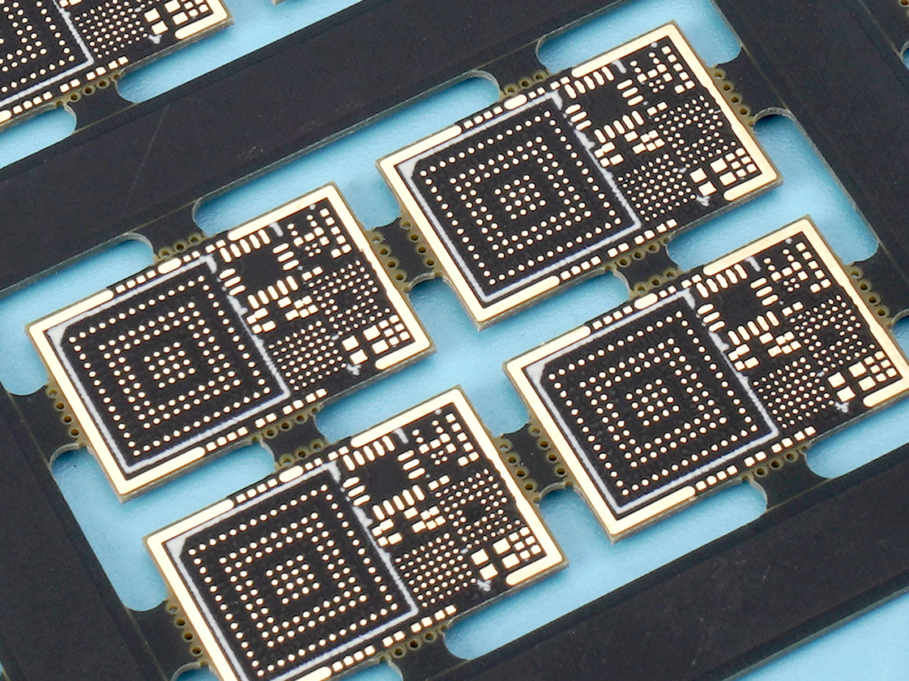
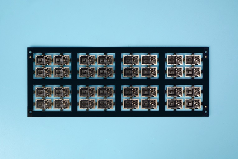
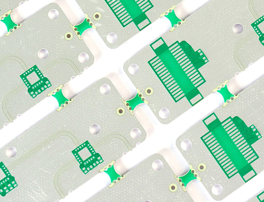
Have you ever seen several small holes on the rails of the PCBs or located at the board edges? They look like trails bites by mouse, do you know what they are? And what’s the function of these? This blog may make you sense about it.
What is Stamp Hole on PCB and its Purpose?
Stamp holes, also sometimes called breakaway holes or mouse bites, are small holes drilled in a row or array along the rails or edges of each circuit board within the panel. They look like the edges of a stamp, so people call it “stamp holes”.
Stamp hole is used primarily in the process of depanelized PCBs. De-paneling is the process of separating individual PCBs from a larger panel, which is a common method in PCB manufacturing to improve production efficiency and reduce costs. The larger panel makes handling and processing multiple PCBs easier during the manufacturing process. In some ways, panel also improves the utilization of the raw materials. Once the manufacturing steps are complete, the individual PCBs need to be separated for use in their corresponding devices. And these holes between the single PCBs can create a weak point along which the boards can be easily broken apart after manufacturing be completed.

Why Use Stamp Holes Expertise In PCBs?
It is possible to use stamp holes if the boards are abnormal shaped or round. The stamp hole is connected between each circuit boards, which mainly plays a supporting role and avoid PCB be scattered. Most commonly, they are used to create PCB stand-alone modules, such as Wi-Fi, Bluetooth, or core board modules, which are then used as stand-alone components placed on another board during PCB assembly.
The use of stamp holes allows for a relatively clean break along the separation line, but it may leave behind rough edges or require additional finishing steps to smooth out the remnants of the perforation points. This method of depaneling is a cost-effective solution and can be used for various types of PCBs, but it might not be suitable for very delicate circuits or when a perfectly smooth edge is required. In addition, V-cut and hollow connection strips also are the common depaneling ways for PCBs.

What are differences between Stamp Hole, V-cut and Hollow strip?
When preparing a panel for the manufacturing of multilayer PCBs, it’s essential to consider a method used to connect individual boards within the panel. As mentioned above, there are three connection methods for PCB technology, each serving different types of PCB designs and requirements. So, which one is the better or how to choose a suitable one for your project? Welcome to keep reading.
V-Cut (V-slot)
V-cut is the most common way to separate the PCBs during the circuit board manufacturing. It mainly utilizes for PCBs with straight edges or straight lines. This method involves cutting a V-shaped groove along the line where two PCBs are connected within the panel. When implemented, V-cuts leave a narrow gap (the width of the V-cut itself) between the boards. V-cut depth is an essential point during the process, make sure it has 1/3 depth on top and bottom side. The V-cut is especially suitable for standard, rectangular PCB designs, allowing for a clean and efficient separation of the boards once all other manufacturing processes have been completed.
Stamp Holes
For PCBs with unique or irregular shapes, stamp holes are often the preferred method of connection. Its process involves drilling multiple small holes in an array at the points where the individual PCBs connect within the panel. These holes create a perforated line that weakens the material enough to facilitate easy separation of the boards by applying minimal force, without compromising the integrity of the circuitry. But this way can only be used if you don’t have strict requirements for burrs on edges. And it is easy to damage the whole board if use improper approach.
Hollow Connecting Strips
Hollow connecting strips are used in scenarios where a very narrow strip of material is left to connect the boards within the panel. This method is particularly useful for PCBs utilizing half-hole (castellated holes) technology. The narrow strips maintain the alignment and integrity of the PCBs during the manufacturing process but can be easily removed or broken away to separate the individual boards. Hollow strip is less common but essential for specific designs and technologies.
Each of these connection methods has its specific applications, advantages, and considerations. The choice between V-cuts, stamp holes, and hollow connecting strips depends on the design of the PCB, the requirements of the manufacturing process, and the desired ease of separation post-manufacturing.
How to Add Stamp Holes on Your Circuit Board?
Designing stamp holes is a critical step in preparing your PCB for the depaneling process. This includes creating a series of small holes along the intended lines of separation between individual boards in a panel. Here’s a step-by-step guide to help you incorporate stamp holes into your PCB design effectively:
1. Understand the Purpose
Recognize that stamp holes are used to facilitate the manual separation of PCBs from a panel after the manufacturing process, minimizing the risk of damage to the board and its components.
2. Plan Your Layout
Placement: Decide where the stamp holes will be located on your PCB layout. They should be placed along the edges where the PCB will be separated from the panel.
Number and Spacing: The number of stamp holes and their spacing can significantly affect the ease of PCB separation. Typically, a distance of 0.5mm between holes and 1.0mm between centers of holes are used, but this may vary based on the PCB material and thickness.
3. Select the Hole Size and Quantity
The diameter of stamp holes usually ranges from 0.6 mm to 1 mm. The size may depend on your specific requirements and the capabilities of your PCB manufacturer. As for quantity, 5-8 holes in an array is good (always 2 arrays/rows), more also is available, it can be adapted based on your specific needs.
4. Arrangement of Stamp Holes
Two rows of stamp holes should be added at the edge of the PCB, extending slightly into the board. This design ensures that any burrs left on the board edge after separation will not affect the PCB’s overall dimensions. If there are traces or other critical components on the edge of the board, ensure that the stamp holes are placed to avoid damaging these elements during separation.
5. Design Using PCB Design Software
Use your PCB design software (such as Altium Designer, Eagle, or KiCad) to add the stamp holes to your design. This can usually be done by placing a series of via or pad holes along the separation lines.
Some software packages may offer tools to automate this process, allowing you to specify the number of holes, their spacing, and diameter, and then automatically place them along a line.
6. Consult with Your Manufacturer
Before finalizing your design, consult with your PCB manufacturer for any specific guidelines or requirements they have for stamp holes. This can include preferred sizes, spacing, and any additional considerations to ensure the depaneling process goes smoothly.
Provide detailed documentation of your stamp hole design to your manufacturer to avoid any confusion during the production process.
7. Review and Adjust
After adding the stamp holes to your design, review the layout to ensure that there is adequate clearance between the holes and any nearby components or traces. This is crucial to avoid damage during the separation process.
Adjust the size, spacing, and number of stamp holes as necessary to meet both your design requirements and the manufacturer’s capabilities.

In the design process, these considerations should be adjusted based on the specific PCB design and manufacturing requirements. Moreover, find a reliable PCB manufacturer to ensure these design details are accurately implemented is key to successfully fabrication.
EBest Circuit (Best Technology) specializes in PCB manufacturing for more than 17 years, offering comprehensive PCB production and design services to over 200 countries worldwide. To ensure the best quality and fast delivery, we set up a strictly quality control system according to ISO9001 and equipped with advanced measured devices such as AOI, X-RAY, 2D, 3D measurement tools in our factory. We provide 24/7 hours service and commitment with a timely reply within 10 hours. We sincerely appreciate your any comments or consults, welcome to contact us at any time.


