pcb
Home > Blog

Posts Tagged ‘surface finishing’

PCB Surface Treatments: A Comprehensive Guide
Tuesday, October 29th, 2024

Printed Circuit Boards (PCBs) are the backbone of modern electronics. To ensure optimal performance and durability, PCBs undergo various surface treatments. These treatments protect the copper traces from corrosion, enhance solderability, and improve the overall reliability of the circuit board. In this article, we’ll explore the most common PCB surface treatments and their applications.

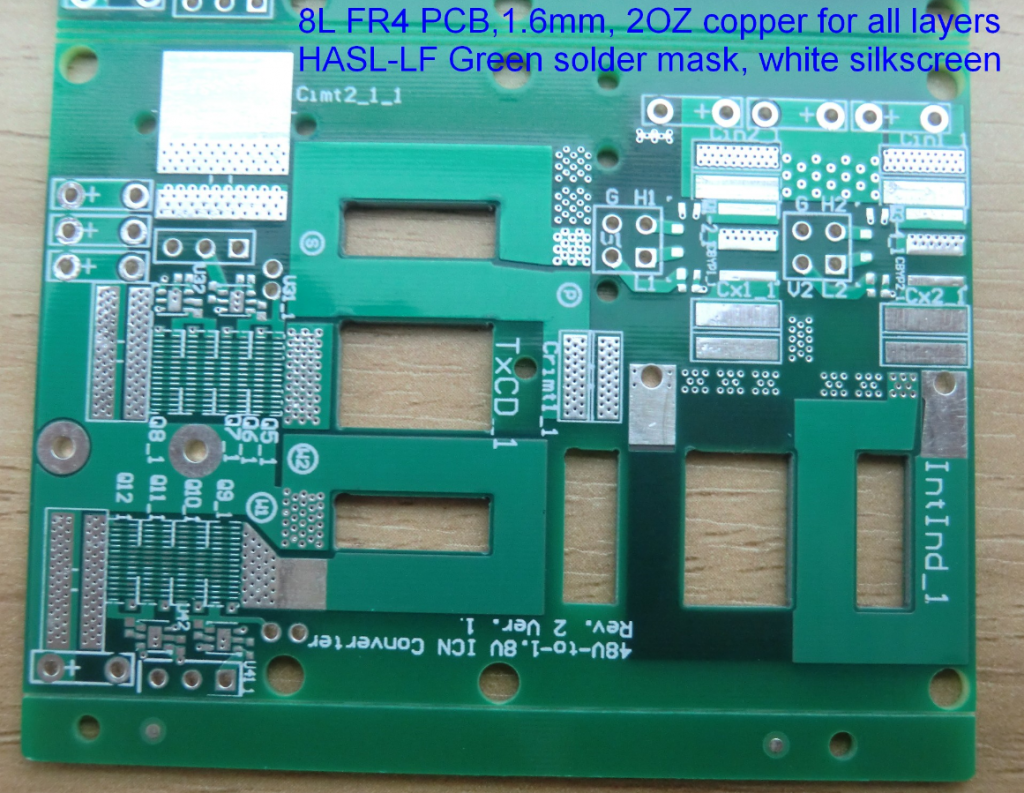
1. HASL (Hot Air Solder Leveling)

    Principle

    HASL is a traditional surface treatment that involves immersing the PCB in a bath of molten solder. After the solder solidifies, hot air is used to level the surface and remove excess solder.

    Features

    •Material: Lead-tin alloy (for traditional HASL) or lead-free solder (for LF HASL).

    •Process: Immersion in molten solder followed by hot air leveling.

    Advantages

    •Excellent solderability.

    •Cost-effective for large volumes.

    •Good mechanical strength.

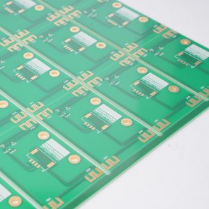
    Picture
    PCB Surface Treatments: A Comprehensive Guide

    2. OSP (Organic Solderability Preservatives)

    Principle

    OSP involves applying a thin layer of organic material (usually a rosin-based compound) to the copper surface, which protects it from oxidation.

    Features

    •Material: Organic preservatives.

    •Process: Application of organic film.

    Advantages

    •Environmentally friendly.

    •Good solderability.

    •Suitable for rework.

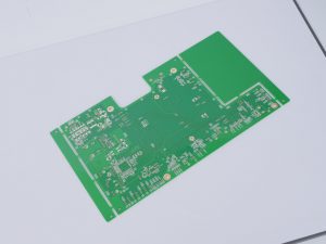
    Picture

    PCB Surface Treatments: A Comprehensive Guide

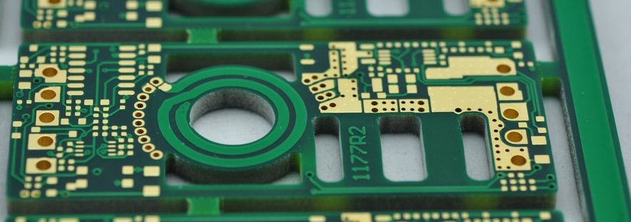
    3. ENIG (Electroless Nickel Immersion Gold)

    Principle

    ENIG involves depositing a layer of nickel followed by a thin layer of gold on the copper surface. This provides a robust barrier against corrosion and ensures good solderability.

    Features

    •Material: Nickel and gold.

    •Process: Electroless nickel deposition followed by immersion gold plating.

    Advantages

    •High reliability.

    •Excellent solderability.

    •Long shelf life.

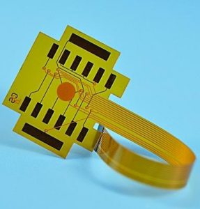
    Picture
    PCB Surface Treatments: A Comprehensive Guide

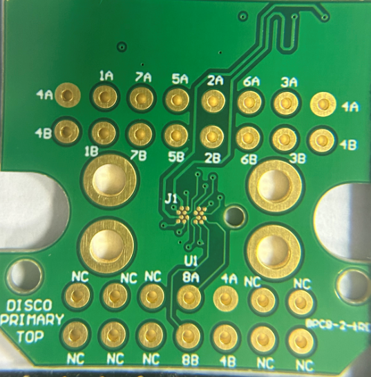
    4. ENEPIG (Electroless Nickel Electroless Palladium Immersion Gold)

    Principle

    ENEPIG is similar to ENIG but adds a palladium layer between the nickel and gold. This improves the resistance to wear and tear.

    Features

    •Material: Nickel, palladium, and gold.

    •Process: Electroless nickel deposition, electroless palladium, and immersion gold plating.

    Advantages

    •Superior wear resistance.

    •Excellent solderability.

    •Long-term reliability.

    Applications

    •High-reliability military and aerospace applications.

    •High-frequency applications.

    •Wire bonding

    Picture
    PCB Surface Treatments: A Comprehensive Guide

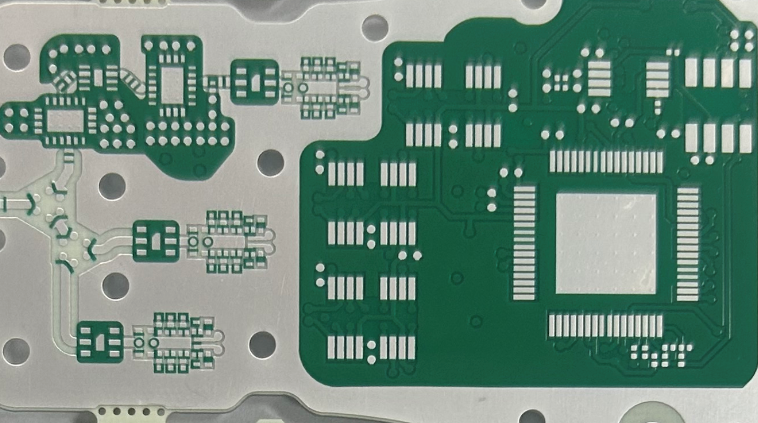
    5. Gold Immersion (Direct Gold Plating)

    Principle

    Gold immersion directly deposits a layer of gold onto the copper surface without a nickel underlayer.

    Features

    •Material: Gold.

    •Process: Direct gold plating.

    Advantages

    •High conductivity.

    •Excellent solderability.

    • Silver Immersion

    Principle

    Silver immersion involves depositing a layer of silver onto the copper surface.

    Features

    •Material: Silver.

    •Process: Immersion silver plating.

    Advantages

    •High conductivity.

    •Low cost compared to gold.

    Picture
    PCB Surface Treatments: A Comprehensive Guide

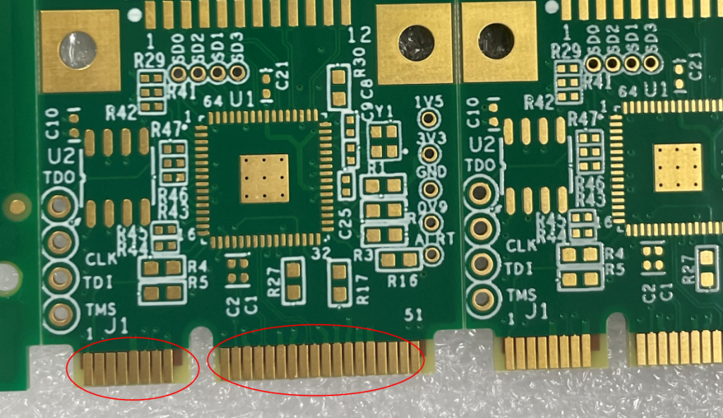
    6. Hard Gold (Selective Gold Plating)

    Principle

    Hard gold is a thicker and harder layer of gold, typically applied selectively to contact areas.

    Features

    •Material: Gold.

    •Process: Selective gold plating.

    Advantages

    •High wear resistance.

    •Good electrical contact properties.

    Picture
    PCB Surface Treatments: A Comprehensive Guide

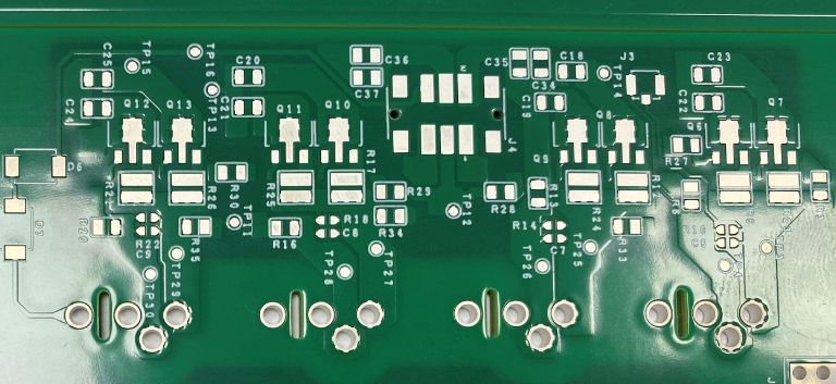
    7. Tin Immersion

    Principle

    Tin immersion deposits a layer of tin onto the copper surface.

    Features

    •Material: Tin.

    •Process: Immersion tin plating.

    Advantages

    •Good solderability.

    •Low cost.

    Applications

    •Cost-sensitive applications.

    •General-purpose electronics.

    Picture
    PCB Surface Treatments: A Comprehensive Guide

    Choosing the right surface treatment for your PCB depends on several factors, including the application environment, cost considerations, and performance requirements. Each treatment has its own set of advantages and limitations. Understanding these treatments will help you make informed decisions that enhance the performance and longevity of your electronic devices.

    I hope this guide helps you understand the different surface treatments used in PCB manufacturing and their applications. If you have any questions or need further clarification, feel free to reach out!

    You may also like

    What Are Differences of ENIG VS ENEPIG in PCB Manufacturing – Series 2
    Tuesday, January 2nd, 2024

    In our last blog, we simply introduced ENIG surface treatment in PCB manufacturing, and this time, we will share more information about the comparison of ENIG and ENEPIG.

    What is ENEPIG Surface Treatment?

    ENEPIG stands for Electroless Nickel Electroless Palladium Immersion Gold. This type of metal coating on the PCB pad surface consists of three layers—nickel, palladium, and gold. Apart from protecting the copper surface from corrosion and oxidation, the ENEPIG surface treatment is also suitable for high-density SMT (Surface Mount Technology) designs.

    For its manufacturing process, manufacturers begin by activating the copper surface, followed by depositing a layer of electroless nickel, then a layer of electroless palladium, and finally, a layer of immersion gold. The process is somewhat similar to the one they follow in the ENIG process, but adding a palladium layer to the ENIG technology. The palladium layer not only improves the surface protection of the PCB, but also prevents nickel from deteriorating and inhibits interactions with the gold layer.

    Pros of ENEPIG Surface Treatment

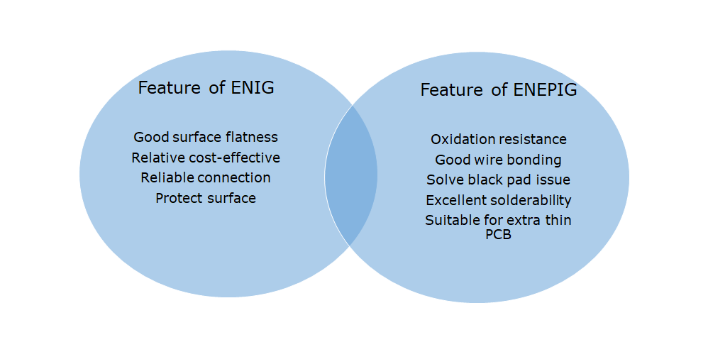
    • Reduce the black pad issues
    • Excellent solderability and high reflow soldering performance
    • Provide high-reliable wire bonding capability
    • High-density design available
    • Meet the miniaturization standards
    • Suitable for extra thin PCBs

    Cons of ENEPIG Surface Treatment

    • Expensive than ENIG process
    • Thicker palladium layer will decrease the effective of SMT soldering
    • Longer wettability time

    What are the Differences Between ENIG and ENEPIG?

    The main difference between ENIG and ENEPIG is the palladium layer. This is the extra layer that added in ENEPIG process, which provides high oxidation resistance, enhance the electrical performance of the surface cleanliness and improve the abrasion resistance of the PCB surface. However, the palladium layer also increases the cost of manufacturing.

    Additionally, the inconsistent surface cleanliness of ENIG, resulting from low solder joint reliability, particularly in gold wire bonding, is a concern. Extra procedures are also required to prevent nickel corrosion in ENIG. When considering it into manufacturing, the ENIG is well-suited for lower-end electronic products.

    (ENIG_VS_ENEPIG)

    The Considerations of Selecting ENIG or ENEPIG Surface Finishing

    Though both two surface treatments offer excellent electrical performance and heat dissipation properties, there are still some conditions that need to consider when choose them.

    • Budget

    Cost is an important factor when choose a suitable surface treatment. As we explain above, ENEPIG is expensive than ENIG, if you are trying to find a relative cost-effective coating, then ENIG is the best choice.

    • End-applications

    The end-applications or finished products also determined the selection of surface finishing. For example, if your PCB will be used in high temperature applications, ENIG would be the better one since it can withstand high temperature.

    • Flatness

    Many traditional surface finishes have poor flatness and smoothness, this brings the big challenge of small-size components mounted. Especially for those fine-pitch components like BGA, an uneven surface can result many problems. However, both ENIG and ENEPIG offer highly smooth surface finishes, forming thin and uniform layers on the solder pads.

    • Bonding demand

    ENEPIG provides the optimal choice for wire bonding due to its highly smooth surface finish, which enhances wire bonding capabilities.

    • Environment-friendly

    Some traditional surface treatments contain hazardous substances, making them non-compliant with RoHS requirements. Both ENIG and ENEPIG made by Best Technology are fully RoHS compliant and lead-free, so you are don’t worry about the environment unfriendly.

    At the end, the choice between ENIG and ENEPIG surface treatments in PCB manufacturing involves a careful consideration of various factors. While both options offer excellent electrical performance, heat dissipation properties, and compliance with environmental standards like RoHS, specific project requirements and priorities will guide the decision-making process. If you are still confuse about the selection of surface treatment, welcome to contact with us, Best Team will give you a best solution that can meet your specific demands and save money for you.

    You may also like

    What Are Differences of ENIG VS ENEPIG in PCB Manufacturing – Series 1
    Tuesday, January 2nd, 2024

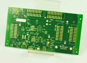
    Surface treatment also called surface finishing, it is a protective layer that through coating a layer of metal organic material on the surface of printing circuit boards (PCBs). Apply a layer of surface treatment enable to protect pads from scratches and oxidation, as well as improve the solderability of components mounting. ENIG and ENEPIG are the two common high-reliable surface finishing types in the circuit board manufacturing, they are not only for FR4-PCB, but also available in ceramic PCB, flex circuits and rigid-flex PCB. Today, Best Team would like to sharing information about ENIG and ENEPIG, and explore the differences between them.

    (Assembled_PCB)

    How to Select the Right Surface Treatment for Your PCB?

    With the rapid development of electronics, there are various of PCB types that can be used in electronic devices, and at the same time, there are also increasingly more surface treatment technics available for selection. Until now, the common surface treatments are OSP, HASL, Immersion Silver, Gold Plating, ENIG and ENEPIG. Each of these surface treatments has its own advantages and disadvantages, so it is necessary to choose the most suitable one for a particular application. The selection of surface finish needs to take into account factors such as cost, application environment, fine-pitch components, the use of leaded or lead-free solder, operating frequency, shelf life, drop and impact resistance, volume and throughput, as well as thermal resistance.

    With PCBs trending towards micro-vias and finer traces, and the drawbacks of HASL and OSP, such as flatness and flux elimination issues, becoming more pronounced, the demand for surface treatments like ENIG continues to grow. In addition, black pad is a major weakness of ENIG while ENEPIG enable to solve it very well, making it a preferred choice for those PCBs need to wire bonding.

    What is the ENIG Surface Treatment?

    ENIG, its full name is Electroless Nickel Immersion Gold, is also known as chemical gold or immersion gold in the electronics industry. This type of surface treatment provides two metal layers—gold and nickel—that manufacturers deposit them on the surface of PCB pads sequentially. This surface finish is a selective surface finish, meaning that certain specific pads may have ENIG surface finish, while others may have different types, such as OSP, HASL, or immersion tin. Here are the main processes of the ENIG coating:

    • Copper activation

    In this step, manufacturers will active the copper layer through cleaning process, this way can help to remove the dust and oxides residual on the surface, but also remove any gases or air trapped in the perforations (holes) of the PCB by wetting the surface. Next, micro-etching the PCB surface using substances like hydrogen peroxide or sulfuric acid.

    • Electroless nickel

    This process is to coat a layer of nickel on the active copper layer by electroplating. The nickel layer serves as a protective layer or inhibitor, which prevent the copper reactive with other elements.

    • Immersion gold

    Immersion gold is the last step of whole ENIG process, immersing the PCB into a mixture, oxidizing the nickel surface, generating nickel ions, and then reducing gold from the mixture. The reduced gold forms a metallic coating to protect the nickel surface. This is the whole process of coating ENIG surface treatment.

    (PCB_with_ENIG_surface_treatment)

    Advantages of ENIG

    • Surface flatness – good for fine-pitch and small size components like BGA.
    • Suitable for press-fit components since it provides a reliable connection for electrical testing.
    • Suitable for wire bonding and gold-fingers connectors.
    • Cost-effective compared with ENEPIG

    Disadvantages of ENIG

    • Black pad issues.
    • Varied coating thickness because of the uncontrolled nickel plated and immersion gold.
    • Poor wettability during PCB assembly.

    All in all, ENIG is a good option if you want to mount fine-pitch components on the PCB surface or if you are considering its use in plug-and-pull devices such as WIFI interfaces. In our next blog, we will introduce ENEPIG surface treatment, including its pros & cons and the differences between ENIG and ENEPIG. Pay attention to our news or contact us directly if you want to know more.

    You may also like