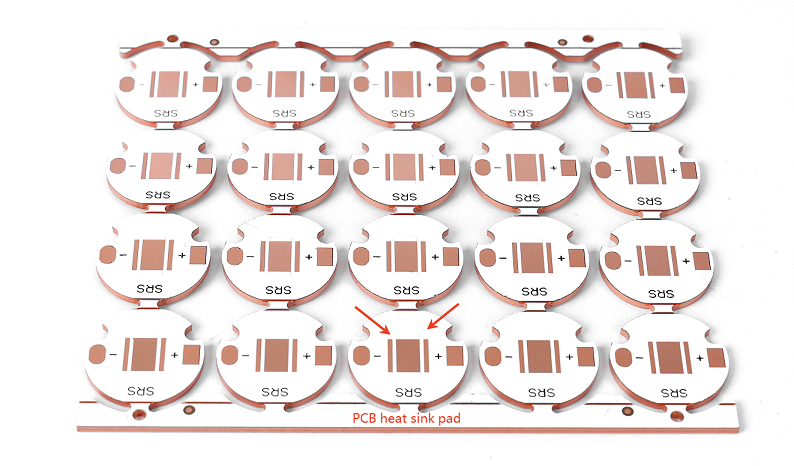
What is PCB Heat Sink Pad?
In high-power electronics, heat is a persistent issue. When left unmanaged, it leads to failure, reduced life span, or poor performance. One of the smart ways to address this is by using a PCB heat sink pad. Sometimes referred to as thermal relief pads, these are conductive areas on a printed circuit board that channel heat away from components. They play a critical role in thermal management, especially in compact and high-density board layouts.
These pads are often seen near power components, processors, or any part prone to heat buildup. By connecting to thermal vias or copper pours, they guide excess heat to ground or large copper areas. Thermal pads improve overall stability without the need for bulky external coolers. A well-designed thermal pad saves cost, space, and ensures better thermal cycling performance.
Importance of PCB Heat Sink Pad
The importance of a PCB heat sink pad lies in its ability to support both thermal and electrical performance. As devices get smaller and more complex, the demand for thermal balance grows. Traditional cooling methods, like fans or heatsinks, aren’t always viable in a tight layout. That’s where these pads step in.
They serve as an internal heat escape path. By reducing the junction temperature of critical parts, the heat sink pad ensures devices function at optimal levels. Without it, hot spots develop, possibly leading to delamination or component drift. In automotive, aerospace, or industrial environments, this can’t be ignored.
Another key advantage is manufacturing. During reflow soldering, thermal pads help maintain consistent heating. This improves solder joint quality, avoiding cold joints or solder bridges.
What Is the Function of a PCB Heat Sink Pad?
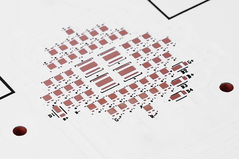
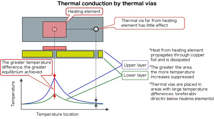
The core function of a PCB heat sink pad is to pull heat away from the component body. This prevents overheating and promotes reliability. A pad usually sits beneath a hot-running device and connects to a ground or power plane through thermal vias. These vias act like vertical pipes that carry heat down to larger copper surfaces.
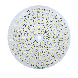
Besides thermal performance, the pad also serves mechanical purposes. It supports the component body, helps with proper alignment during placement, and aids in reflow stability. In power ICs, LEDs, and RF modules, such a pad is more than a convenience—it’s a necessity.
Often placed under QFNs, D-Pak, or Power MOSFETs, thermal pads are essential for packages where direct contact to the PCB is required for heat dissipation.
PCB Thermal Pad vs Heatsink
Understanding the thermal pad vs heatsink comparison helps in design decisions. A thermal pad (on PCB) is a built-in copper area, often plated and connected via thermal vias. It is internal and does not add extra height to the device. It’s subtle, efficient, and passive.
A heatsink, on the other hand, is a physical attachment—usually a metal block or finned structure—mounted on top of the component. It dissipates heat through air convection. While highly effective, heatsinks increase weight and require space. They may also need fasteners or thermal paste for better performance.
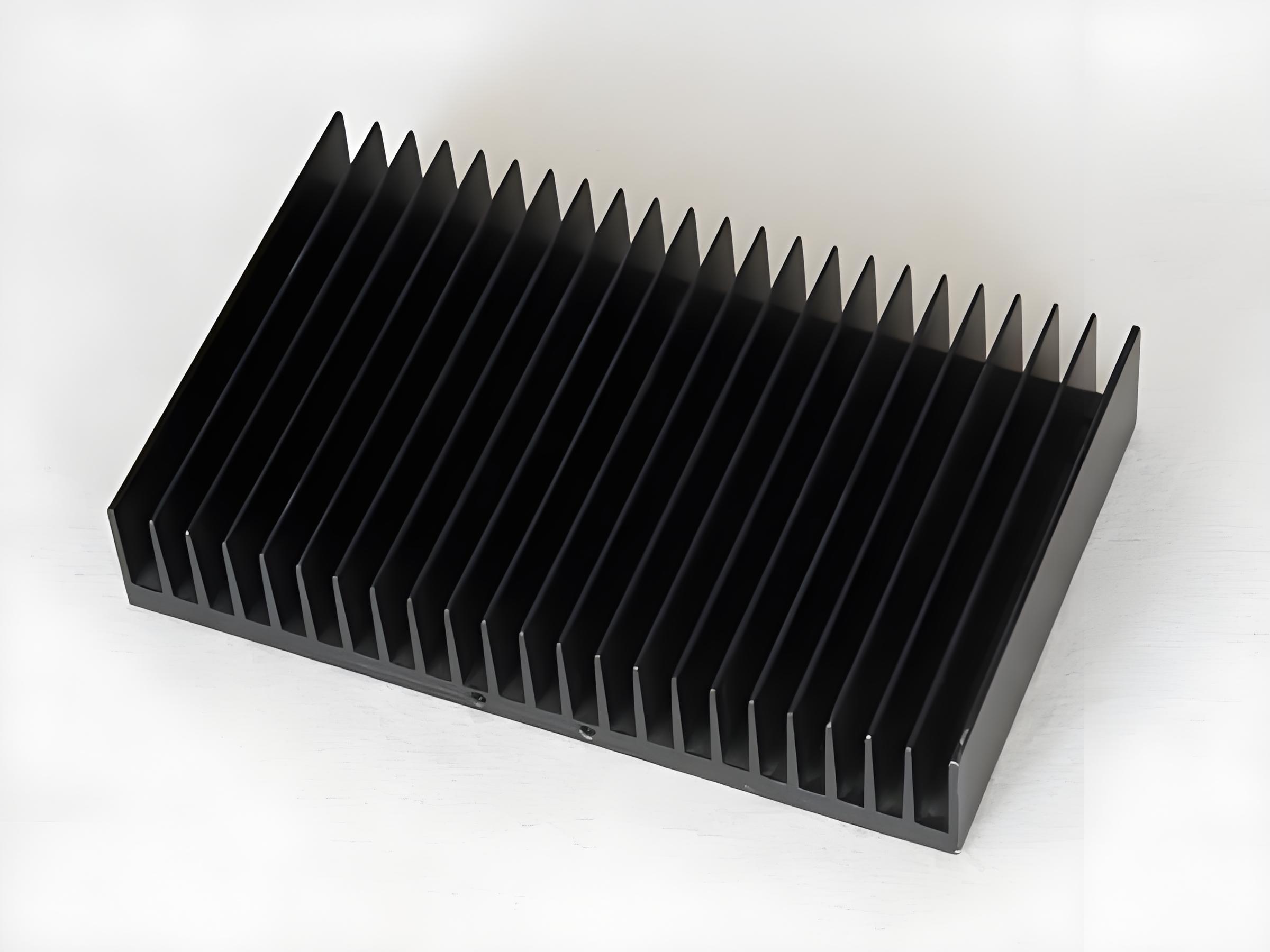
In low to medium-power circuits, thermal pads do the job silently. When current levels increase or the ambient conditions are harsh, heatsinks may be added. However, both solutions often work together. A pad draws the heat from the chip, and the heatsink then transfers it to the air.
Why Do We Need Thermal Pad on PCB?
We need thermal pads on PCBs to manage heat efficiently within confined board layouts. As chips grow more powerful and boards become smaller, heat density rises. Left unchecked, this can stress the materials, warp the PCB, or trigger thermal shutdowns in sensitive ICs.
Thermal pads provide a compact and cost-effective solution. Unlike external cooling systems, these pads are part of the board design. They reduce the thermal resistance between the component and the ground plane, making heat transfer faster and more efficient.
In LEDs, they stop lumen drop due to temperature spikes. In CPUs or RF amplifiers, they prevent drift in performance. Across industries, from smartphones to satellites, thermal pads are silent protectors against damage caused by thermal fatigue.
Design Consideration of Thermal Relief Pads on PCB
The design of thermal relief pads is not just about placing a copper square under a part. It demands precision. Several factors shape the design.
1. Pad Size: The area should match the component’s thermal tab. Oversized pads can cause solder wicking; undersized ones fail to transfer heat efficiently.
2. Vias Count and Diameter: Vias enhance heat transfer. Placing multiple small vias (0.3mm diameter with 6+holes) within the pad connects it to inner or bottom layers. These must be filled or tented to avoid solder leakage.
3. Copper Weight: Thicker copper layers enhance thermal conduction. A 2oz or 3oz copper layer works better than standard 1oz in high-heat zones.
4. Solder Mask Clearance: The pad must be free from mask to allow full thermal contact.
5. Connection to Planes: The pad should tie to ground or power plane, depending on the circuit. Use thermal relief spokes when needed to balance heat dissipation and solderability.
6. Component Package Type: Each package, whether QFN or TO-263, demands unique pad sizing and via patterns. Manufacturer datasheets offer recommended layouts—follow them closely.
When to Use Thermal Relief PCB?
Using a thermal relief PCB becomes necessary in several scenarios. One key use is in multilayer boards where copper planes absorb too much heat. Without thermal relief, soldering becomes difficult as heat spreads too quickly. This leads to cold joints or poor wetting.
Thermal reliefs help balance the heat flow. They allow soldering while still ensuring strong thermal performance. Another situation arises with through-hole components connected to large copper areas. Thermal relief spokes prevent the pad from acting like a heat sink during soldering.
Power applications like inverters, motor controllers, and regulators benefit from thermal relief PCBs. So do high-brightness LED arrays. In RF boards, where impedance matters, thermal pads also stabilize the electrical response by providing consistent grounding.
Use them when heat buildup could impair function or reduce board life. Proper relief design improves both manufacturing and operational performance.
What Does Best Technology Offer?
At Best Technology, we provide high-performance thermal solutions that elevate your product’s efficiency and reliability. With over 18 years of industry leadership, our expertise in PCB heat sink pads and thermal relief pads ensures your devices stay cooler, last longer, and perform better under pressure. Whether you’re in aerospace, automotive, or consumer electronics, we deliver custom-designed metal core PCB solutions that meet your most demanding thermal management needs.
In additional to design thermal pads on PCB to achieve high heat dissipation, we also offer ceramic PCB and metal core PCB (including aluminum PCB, copper core PCB, sinkpad PCB), which have very good thermal conductivity to dissipate the heat fastly. If you want to know more about metal core PCB, ceramic PCB or thermal pads design guide, you are welcome to leave your comments below or contact us at sales@bestpcbs.com.