

Ceramic PCBs are a special breed of printed circuit boards known for their exceptional thermal resistance and durability. These PCBs are used in industries where high performance is critical, such as aerospace, automotive, medical devices, and power electronics. Nowadays, the most common types of ceramic PCB are thick film, DCB, DPC, AMB, HTCC, LTCC and thin film. In this article, we will introduce each of them in details.

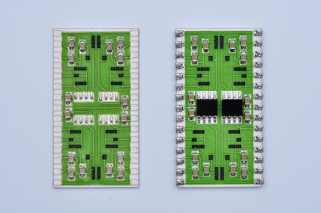
Thick Film Ceramic PCB
Thick film technology is a process by using screen printing conductor paste and directly deposit slurry (conductor) on the ceramic substrate. Then sintering it under high temperature to form conductive circuit traces and electrodes, which is suitable for most ceramic substrates.
After the material is sintered at high temperature, a strong adhesion film will be formed on the ceramic circuit board, repeat this step for many times, a multi-layer circuit is generated.
You can print resistor or capacitor on the surface to get a interconnected structure. At Best Technology, we can make all the resistors with the same value, or different value for different resistor on the same board.
Thick film ceramic PCB has advantages on the simple manufacturing process, but it has some drawbacks that can’t be ignored:
- Limited by the conductive paste and screen size
- Line width less than 100um is difficult to achieved
- Three-dimensional patterns are not available
- Not suitable for fine-trace project
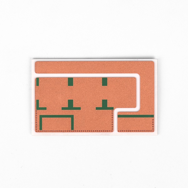
DBC / DCB Ceramic PCB
Direct Bonded Copper (DBC) or Direct Copper Bonded (DCB) ceramic PCBs are known for their excellent thermal conductivity. They are made by bonding a layer of copper directly onto a ceramic substrate, typically aluminum oxide or aluminum nitride. Due to the DBC technology is directly bond copper on the ceramic substrate, it can achieve thicker copper thickness to 300um. So, it is very suitable for high power applications.
The basic chemistry principle is to introduce an appropriate amount of oxygen between copper and ceramics before or during the application process. Copper and oxygen will form Cu-O eutectic liquid under 1065℃~1083℃. This is an important element in the manufacturing. DBC ceramic circuit board uses this eutectic solution to chemically react with the ceramic substrate to form CuAlO2 or CuAl2O4, achieving the combination between substrate and copper foil.
However, it is easy to generate micro-porosity between Al2O3 and Copper during the copper bonded process, and it doesn’t have a good solution by far. That is why the yield of DBC ceramic PCB is not good than DPC.
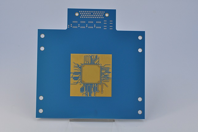
DPC (Direct Plated Copper Ceramic PCB)
DPC ceramic PCB utilizes direct copper plating technology, deposit copper foil on the alumina oxide (Al2O3) substrate. It is the most commonly used ceramic PCB in recent years. The circuit generated process is: pre-treatment – sputtering – exposure – develop – etch – strip – electroplating.
AMB (Active Metal Brazed Ceramic PCB)
AMB ceramic copper clad plate adopts the active brazing process, and the copper layer bonding force is higher than that of DPC, which is around 18n/mm – 21n/mm. AMB ceramic copper clad plate usually has a high binding force, usually makes thicker copper, between 100um and 800um. The AMB ceramic PCB generally rarely design traces or holes, even if there is a trace is very simple, the spacing is relatively wide.
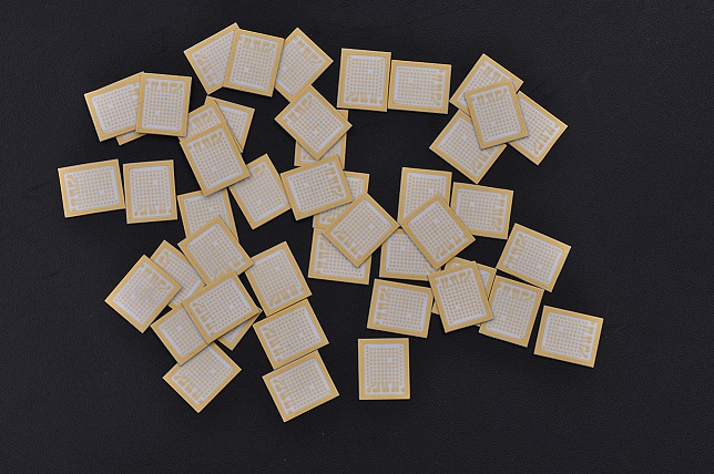
HTCC (High Temperature Co-fired Ceramic PCB)
HTCC is a relatively early development technology, but due to the high sintering temperature (1300~1600℃), the choice of electrode materials is limited. Meanwhile, its cost is more expensive, these promotes the development of HTCC is relatively slow.
LTCC (Low Temperature Co-fired Ceramic PCB)
Although LTCC reduces the co-firing temperature to about 850 ° C, the disadvantage is that the dimensional accuracy and product strength are not easy to control.
Thin Film Ceramic Circuit Board
The thin film ceramic PCB is to deposit a metal layer directly on the surface of substrate by sputtering process. Through lithography, development, etching and other processes, the metal layer can also be graphed into a circuit pattern. Due to the low deposition speed of sputtering coating (generally less than 1μm/h), thin film substrate surface metal layer thickness is small and can prepare high pattern accuracy (line width/line space less than 10μm).
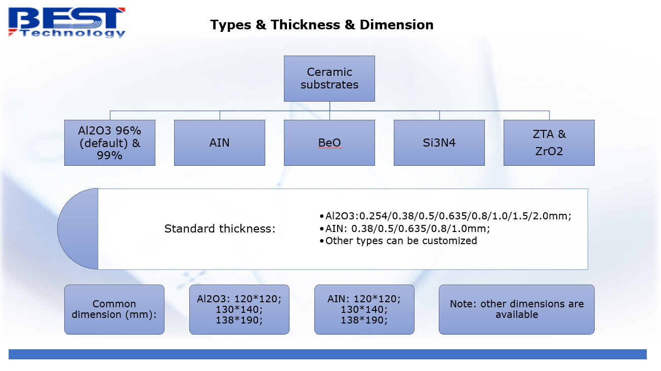
Common Ceramic Substrates
Best Technology is a leading ceramic PCB manufacturer in Asia, our core members has over 20 years manufacturing experience in ceramic PCB fabricating. “High mixed, low volume, high quality, fast delivery” is our advantages and we always try our best to do that, make ourselves better and better. If you are interested in it, feel free to contact us, we are always online.