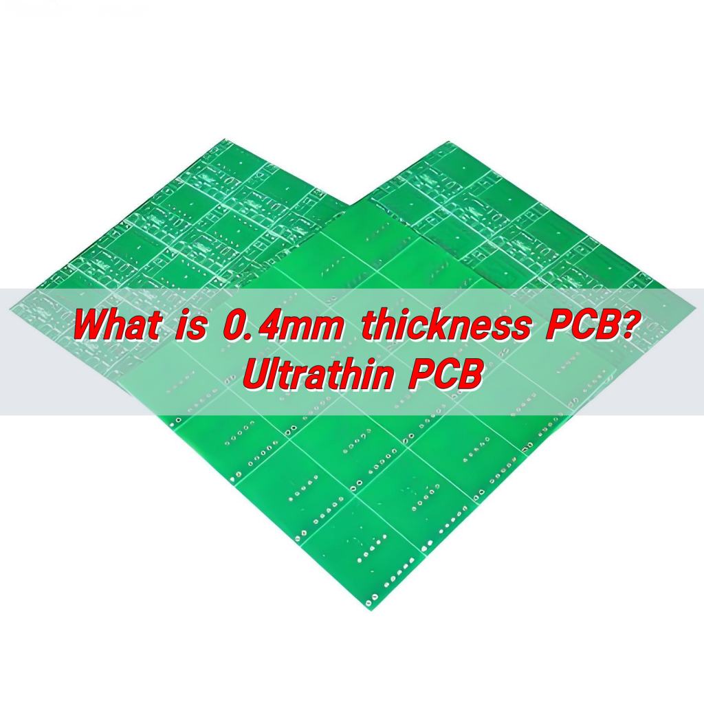
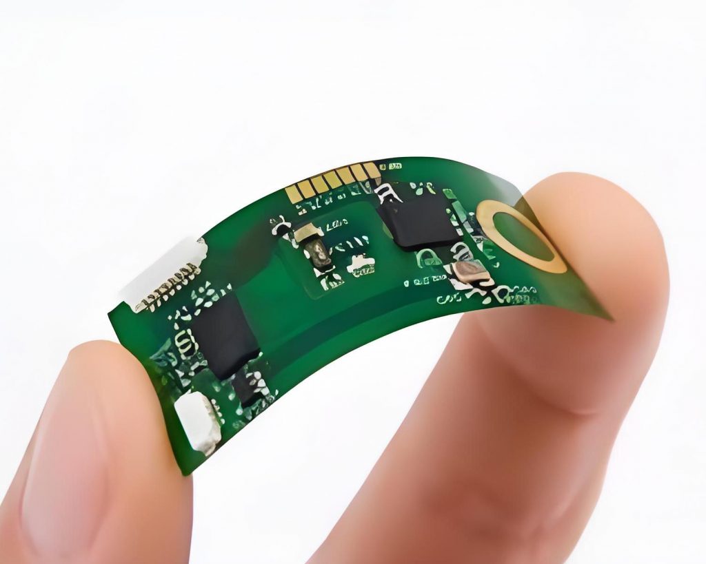
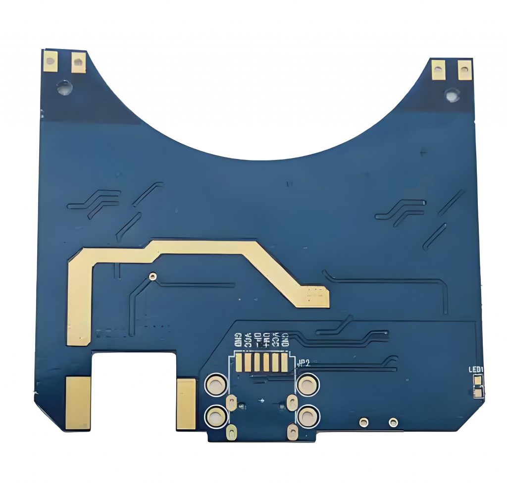
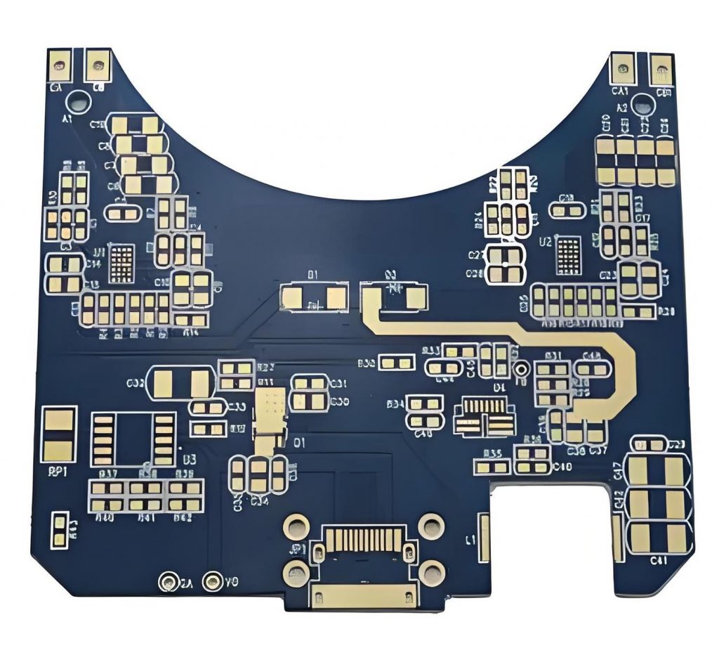
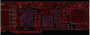
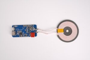
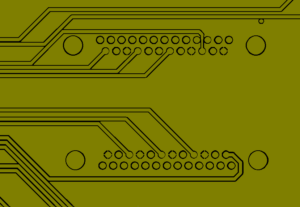
What is 0.4mm thickness PCB? 0.4mm thickness PCB is an ultra-thin printed circuit board with a thickness of only 0.4 mm. This type of PCB has high requirements in design and manufacturing, because its thinness makes it easy to cause problems such as warping and deformation during processing. 0.4mm thickness PCB is usually used in electronic devices with strict requirements on space and weight. It can meet the development trend of miniaturization and thinness of modern electronic products.
What is a 0.4mm Thickness PCB?
A 0.4mm thickness PCB refers to a printed circuit board with a thickness of 0.4 mm. This thickness of PCB is generally considered to be the minimum thickness starting point for multi-layer PCB design, suitable for application scenarios that require highly integrated and compact design.
0.4mm PCB has the following characteristics:
- Thin design: Suitable for electronic products that require highly integrated and compact design, such as smartphones, tablets and other portable devices.
- High reliability: Due to its thin design, 0.4mm PCB performs well in complex wiring and fine design, and can provide stable electrical performance and mechanical strength.
- Cost-effectiveness: Although the manufacturing process is more complicated, the overall cost is relatively low because it uses less material.
0.4mm PCB is mainly used in the following fields:
- Portable devices: Such as smartphones, tablets, wearable devices, etc., which require lightweight and powerful circuit boards.
- High-density interconnect applications: In occasions where high integration and complex wiring are required, 0.4mm PCB provides a better solution.
- Radio frequency identification (RFID) and smart cards: Such as RFID tags, IC cards, SIM cards, etc., these applications require circuit boards that are both thin and reliable.
What are the advantages of 0.4mm thickness PCB?
0.4mm thickness PCB has the following advantages:
- Reduced material cost: Due to the use of less expensive materials such as copper, the material cost of 0.4mm thickness PCB is lower.
- Compatibility with advanced technologies: PCBs of this thickness are compatible with advanced technologies such as laser direct imaging and can be used without damaging flexible circuits.
- High reliability: Ultra-thin PCBs can host custom repeatable routing paths, reduce rework, and have higher reliability.
- Strong protection: The conductors on these PCBs have a polyimide cover layer to protect against a range of potentially harsh conditions, such as vibration and acceleration on the joints.
- High durability: 0.4mm thick PCBs can withstand millions of bending cycles and are suitable for applications that require frequent bending.
In addition, 0.4mm thick PCBs are suitable for a variety of application scenarios, including RFID smart cards, IC cards, SIM cards, electronic tags, mobile phone charging modules, wearable devices, etc.
What are the disadvantages of 0.4mm thickness PCB?
The disadvantages of 0.4mm thickness PCB mainly include the following aspects:
- Difficulty in manufacturing: Due to the thinness of 0.4mm thickness PCBs, they are easily affected by external factors during the manufacturing process, which increases the difficulty and cost of manufacturing.
- Lower mechanical strength: Thinner PCBs are more likely to deform or be damaged when subjected to external forces, especially in environments with high-frequency vibration or mechanical shock, which may affect their stability and reliability.
- Poor heat dissipation: Thinner PCBs have a relatively small heat dissipation area, which is not conducive to the rapid dissipation of heat, and may cause local overtemperature, affecting the stable operation of electronic components.
- Increased welding difficulty: During the welding process, thinner PCBs are easily affected by the welding temperature, which may cause loose welding points or welding defects.
- Signal transmission problems: Thinner PCBs may affect the integrity and transmission speed of signals due to the shorter signal path when transmitting high-frequency signals.
How to make 0.4mm thickness PCB?
There are many aspects to consider when making 0.4mm thickness PCBs.
1. Material selection
- Substrate: Select a substrate suitable for 0.4mm thickness. Generally, 0.3mm raw materials are used to make 0.4mm PCB boards. The type of substrate is usually FR-4 or other materials suitable for thin boards.
- Copper foil thickness: The thickness of the copper foil affects the conductivity and strength of the PCB. Common copper foil thicknesses include 1 ounce (about 35 microns), 2 ounces (about 70 microns), etc.
2. Production process
- Cutting: Cutting large-sized copper foil boards into small pieces suitable for production.
- Drilling: Drilling is the first process for the formal production of circuit boards, including electrical holes, mechanical holes, vias, etc. For 0.4mm thick PCBs, laser drilling may be required to achieve smaller apertures.
- Lamination: By combining different core thicknesses and prepreg sheets, a finished PCB thickness of 0.4mm can be achieved.
- Electroplated: Electroplated after drilling to ensure good conductivity in the hole.
- Solder mask: Add a solder mask to the surface of the PCB to protect the copper wire from oxidation and prevent short circuits during welding.
- Surface treatment: Common surface treatment methods include immersion gold, tin spraying, etc. to improve the conductivity and oxidation resistance of the PCB.
What are the difficulties in making a 0.4mm thick PCB?
The main difficulties in making a 0.4mm thick PCB include the following aspects:
- Lamination difficulties: As the copper thickness increases, the line gap is deeper, and more resin filling is required, which increases the complexity and cost of processing.
- Drilling difficulties: As the board thickness increases, the drilling difficulty increases. Thick copper boards are usually thicker than 2.0mm, and new knives and segmented drilling techniques are required to reduce the difficulty when drilling.
- Thermal management: Due to the increase in power consumption of electronic devices, thermal management has become a key challenge. When designing, it is necessary to consider appropriate heat dissipation structures and heat dissipation component layouts to ensure that components work properly and avoid thermal damage.
- Signal integrity: High-frequency signals and high-speed digital signal transmission need to consider issues such as signal loss, impedance matching, and interlayer crosstalk.
- Electromagnetic compatibility (EMC) and electromagnetic interference (EMI): Measures need to be taken to reduce electromagnetic radiation and improve anti-interference capabilities.
- Process and material selection: Choose the appropriate printing method and substrate material to ensure that the circuit board that meets the requirements is manufactured.
How to deal with the warping problem of 0.4mm thick PCB?
There are several ways to deal with the warping problem of 0.4mm thick PCB:
- Choose high Tg board: Boards with higher Tg can withstand higher temperatures and reduce warping caused by temperature changes. Although the cost is higher, it can effectively resist high temperature deformation.
- Reduce via restrictions: The via design in multilayer boards should be reasonable to avoid excessive restrictions on the cold expansion and contraction of the board and reduce warping.
- Control temperature changes: Appropriately reduce the reflow temperature or slow down the heating and cooling speed to reduce the expansion and contraction of materials caused by temperature changes.
- Use laser drilling technology: Laser drilling can reduce stress during processing and reduce the risk of warping.
- Mechanical leveling: Use a flattening machine to mechanically level the PCB, which is suitable for PCBs with moderate warping.
The following aspects can be used to deal with the warping problem of 0.4mm thickness PCB:
What should I pay attention to when using 0.4mm thickness PCB?
The following points should be noted when using 0.4mm thickness PCB:
- Trace spacing and width: On 0.4mm thickness PCB, the trace spacing is usually recommended to be no less than 0.2mm to ensure stable signal transmission and reduce interference. The trace width should be designed according to the current carried. Usually the width of the power line should be between 1.2~2.5mm, and the width of the signal line should be between 0.2~0.3mm.
- Wiring rules: In high-density and high-precision PCB design, the line width and spacing are generally set to 0.3mm. If solder mask defined (SMD) pads are used, the thickness of the traces between the pads should be appropriately reduced to avoid the problem of pad lifting during soldering or desoldering.
- Heat dissipation and mechanical support: For devices with high power consumption, 0.4mm thick PCBs may not be enough to provide sufficient mechanical support and heat dissipation performance. For such devices, it is recommended to choose a thicker PCB to provide better mechanical support and heat dissipation performance.
- Design details: When designing the PCB, it should be noted that the spacing between components should be greater than 0.5mm, and the spacing between the chip pins and peripheral devices should be greater than 1.0mm. In addition, the width of the ground line should be greater than the power line to ensure a stable current supply.
0.4mm thick PCB has become an ideal choice for modern electronic products such as smartphones and wearable devices due to its ultra-thin characteristics, meeting the development needs of miniaturization and thinness. However, problems such as warping are prone to occur during production. As a professional PCB manufacturer, BEST Technology has strong manufacturing strength to ensure that each 0.4mm thick PCB effectively reduces the occurrence of warping. If you have corresponding needs, please feel free to contact us at sales@bestpcbs.com!


