Vias Plugged PCB has become a common technique to improve the integrity and functionality of a board in the world of PCB (Printed Circuit Board) manufacturing. This process involves filling or sealing the holes, known as vias, which are used to create electrical connections between different layers of a PCB. But why is via plugging so important, and what does it involve? In this blog, we’ll dive into what via plugging is, the different types of vias, and its role in PCB design and performance. Let’s explore the various aspects of this technique and its significance in the world of PCB production.

What is Via Plugging in PCB?
Via plugging is the process of filling or sealing vias, which are holes drilled into a PCB to establish electrical connections between different layers. These vias can be plugged for various reasons, such as preventing unwanted signals from traveling through the vias or ensuring better protection against environmental factors like moisture. The plugging material used may vary, but most commonly, it’s a resin, green oil, or solder mask. The plugged vias add structural integrity to the PCB and enhance its electrical performance.
What Are the Different Types of Vias in PCB?
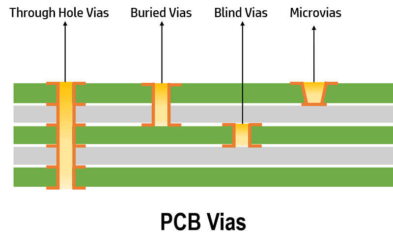
PCBs can have several types of vias, each designed for specific purposes. The main types include:

Through-hole Vias: These are the most common vias, which pass through the entire board and connect all the layers.
Blind Vias: These connect an outer layer to one or more inner layers but do not pass through the whole PCB.
Buried Vias: These are located entirely within the PCB and do not reach the outer layers, offering a more compact design.
Micro Vias: Smaller than standard vias, they are used in high-density interconnects (HDI) PCBs to create intricate circuits.
Each type of via has its own purpose and is selected based on the design requirements of the PCB.
What’s the Purpose of Vias in PCB?
Vias serve several critical functions in PCB design. Their primary purpose is to provide electrical connections between different layers of the board. This allows signals to travel between top, bottom, and inner layers, creating complex and multi-layer circuits. Vias are also essential for thermal management, helping to dissipate heat across the PCB, ensuring it operates efficiently and remains within temperature limits.
What is the Difference Between Via Plug and Via Fill?
While both processes involve filling vias, they are slightly different in their application. Via plugging refers to sealing the via to prevent signal interference or to fill the via with a non-conductive material, such as resin or solder mask. Via filling, on the other hand, is typically done with a conductive material to ensure that the via still maintains an electrical connection, especially in high-frequency or high-performance PCBs.
What is the Difference Between Tented Via and Untented Via?
A tented via is a via that is sealed with a solder mask over the hole to protect it from environmental damage. This method is often used to prevent moisture or contaminants from entering the via. On the other hand, an untented via remains open and unsealed. Tented vias are commonly used in consumer electronics where the environment is relatively controlled, while untented vias may be seen in applications where electrical continuity is more critical than protection.
What is the Difference Between a PCB Hole and a Via?
The primary difference between a PCB hole and a via lies in their function. A PCB hole is simply a hole in the board, often used for mechanical purposes, such as mounting or securing components. A via, however, is specifically designed for electrical connections between the different layers of the PCB. While holes can be part of a PCB design, vias play a much more specific and functional role in the overall circuit design.
Do Vias Increase PCB Cost?
Yes, vias can increase the cost of manufacturing a PCB. The more complex the via design (e.g., blind or buried vias), the higher the cost due to the additional drilling and processing required. Moreover, the use of via plugging materials, such as resins or green oil, also adds to the cost. However, despite the cost increase, vias are often necessary for high-performance PCBs, especially those used in complex electronics, where the design requirements outweigh the cost considerations.
When to Use Vias in PCB?
Vias are used in PCBs when there’s a need for multi-layered designs or when connecting different electrical components across multiple layers is required. They are often used in high-density and high-frequency PCBs, such as those found in smartphones, computers, and medical devices. If you are designing a PCB that needs to be compact but complex, vias will be essential for providing the necessary electrical connections without compromising space.

Via plugging is an essential process in PCB manufacturing that contributes to both the functionality and durability of the board. Whether you’re working with through-hole, blind, buried, or micro vias, plugging them at the right time and with the right materials ensures that your PCB will perform optimally. By understanding the different types of vias and how they contribute to the overall design, you can make more informed decisions about when and how to use them in your PCB projects.
At EBest Circuit (Best Technology), we specialize in high-quality PCB manufacturing, offering a range of solutions for your project needs. From via plugging to precision design, we ensure that every PCB we produce meets the highest standards of performance and reliability. If you’re looking for a trusted partner for your PCB needs, reach out to us today at sales@bestpcbs.com!


