What is Ceramic PCB
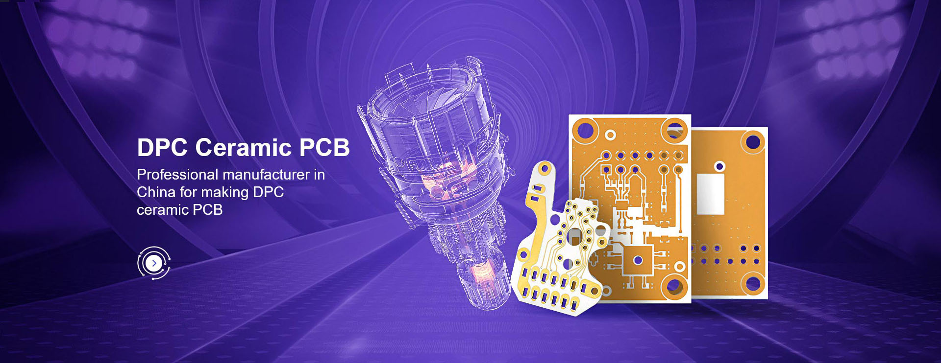
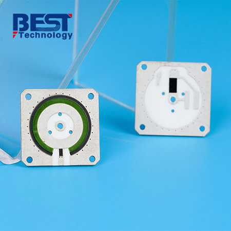
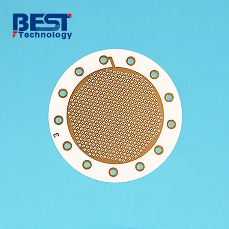
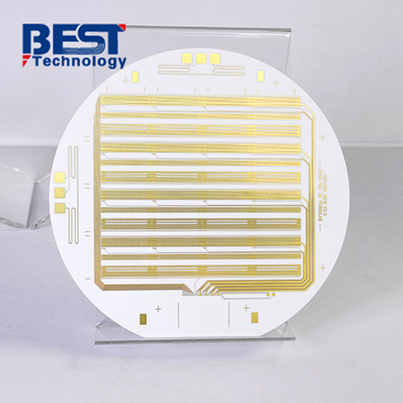
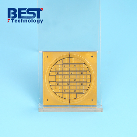
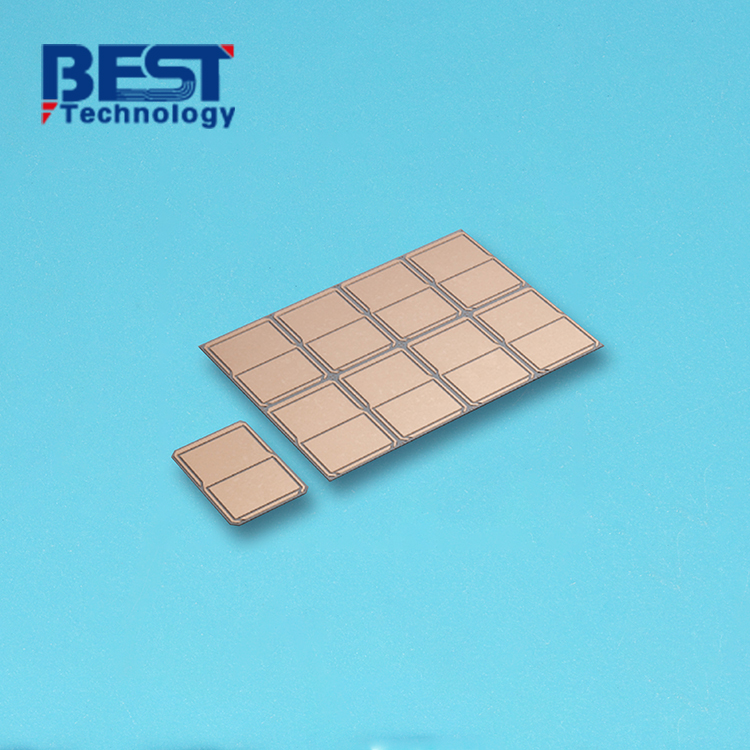
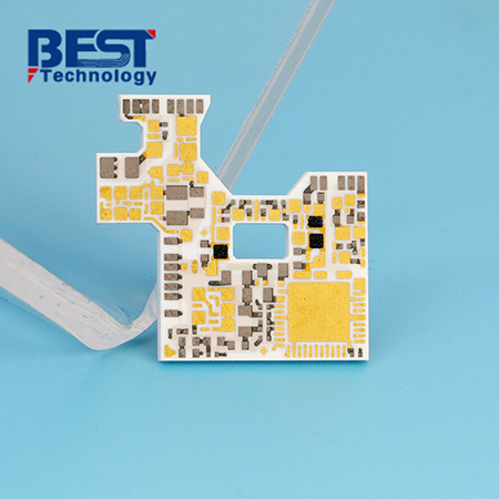
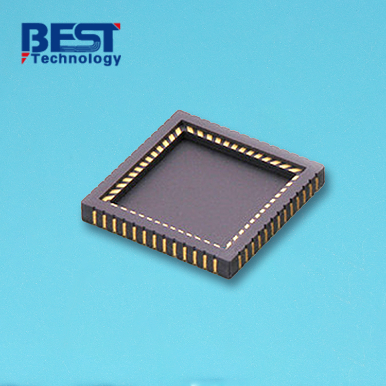
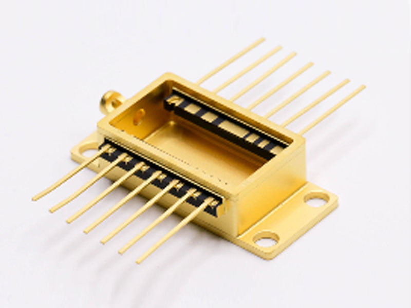
ceramic substrate pcb,ceramic pcb boar,Ceramic PCB is an advanced circuit board that is manufactured using ceramic materials, unlike traditional circuit boards made of organic materials such as fiberglass or epoxy resin.
Ceramic PCBs have excellent performance and reliability, especially in demanding high-performance electronic applications. These boards are designed to excel in situations where high thermal conductivity, excellent electrical performance at high frequencies, and robustness in harsh environments are critical.
The manufacture of ceramic PCBs utilizes thermally conductive organic ceramic powders and organic adhesives, prepared at less than 250°C, with a thermal conductivity of 9-20W/m.k. In addition, ceramic PCBs are bonded together by bonding copper foil and ceramic substrate, which has strong bonding and the copper foil will not fall off, so the performance is stable and the reliability is high in high temperature and high humidity environments.
What is the maximum temperature for a ceramic PCB?
Traditional PCB boards can usually only withstand high temperatures of 100-200°C. Ceramic PCB boards are resistant to high temperatures. The boards are generally made of alumina ceramic base or aluminum nitride ceramic base and can withstand 800-2200°C.
Alumina ceramic PCB boards can withstand high temperatures of 800°C,
Aluminum nitride ceramic PCB boards can withstand high temperatures of 2200°C.
How thick is ceramic PCB?
The thickness of ceramic PCB ranges from 0.25mm to 3.0mm.
The thickness of ceramic PCB mainly depends on its application field and design requirements. Conventional board thicknesses include 0.25mm, 0.38mm, 0.635mm, 0.8mm, 1.0mm, 2.0mm and 3.0mm, etc. These thicknesses include the thickness of the board itself and the additional thickness of the process layer (such as circuit, solder mask, copper thickness, surface treatment, etc.) Therefore, the finished thickness of ceramic PCB is the thickness of the board plus the thickness of the process layer.
ceramic pcb material
Ceramic PCBs have different types of substrates, such as alumina, aluminum nitride, silicon nitride and silicon carbide, each with its own characteristics of thermal conductivity, strength, insulation, etc. When choosing a ceramic PCB, you need to consider power, temperature, cost and manufacturing difficulty.
Alumina PCBs are commonly used, with good thermal conductivity and low cost;
Aluminum nitride PCBs have high thermal conductivity and are suitable for high-power devices;
Silicon nitride PCBs have high strength and are suitable for high temperature and vibration environments;
Silicon carbide PCBs are resistant to high temperatures and are used in the laser field.
ceramic pcb manufacturing process
- Design and Layout: The process starts with the design of the circuit layout using computer-aided design (CAD) software. Components, traces, vias, and other elements are placed and routed on the layout, taking into account factors such as thermal management and signal integrity.
- Substrate Preparation:
Ceramic substrates are selected based on the requirements of the application, such as thermal conductivity and electrical properties. Ceramic substrates are prepared by cutting, forming, and polishing to the required size and surface finish.
- Layer Preparation (for multi-layer PCBs):
For multi-layer ceramic PCBs, individual ceramic layers are prepared and manufactured. These layers will eventually be stacked and interconnected. Each layer can go through processes such as screen printing, where conductive and insulating pastes are applied to create circuit traces and insulating layers.
- Conductive Layer Deposition:
Conductor material, usually a metal paste containing silver or gold particles, is applied to the substrate using techniques such as screen printing or inkjet printing. These conductive traces will carry electrical signals between components.
- Via Drilling and Filling:
Via holes are small holes that connect different layers of a PCB and are drilled using laser or mechanical drilling techniques. The vias are then filled with conductive or non-conductive materials to establish connections between layers.
- Firing or Sintering:
The ceramic substrate coated with conductive material is fired in a high-temperature furnace. The process sinters the ceramic and fuses the conductive material to form a strong and durable circuit structure.
- Additional Layering (for Multilayer PCBs):
The process of applying conductive traces, insulating layers, and vias is repeated for each layer in the multilayer stack.
- Component Attachment:
Components such as surface mount devices (SMDs) are attached to ceramic PCBs using solder or specialized adhesives. Due to the high thermal conductivity of ceramics, specific soldering techniques may be required to ensure proper bonding.
- Testing and Inspection:
Assembled ceramic PCBs undergo a variety of tests, including continuity checks, electrical tests, and potential environmental tests. The inspection process helps identify defects and ensure the functionality and reliability of the PCB.
- Finishing and Coating:
- Final Testing:
The finished ceramic circuit board undergoes final functional testing to ensure that it meets the specified requirements and operates correctly.
- Packaging and Delivery:
After the ceramic PCB passes all tests and inspections, it will be packaged and ready for delivery to customers or further integration into electronic devices.
What is a ceramic PCB used for?
Aerospace: The high performance characteristics of ceramic PCB make it an indispensable electronic component in the aerospace field, ensuring the reliable operation of avionics equipment under extreme conditions.
Military: In military applications, the durability and stability of ceramic PCB are essential to ensure the long-term reliable operation of equipment, especially in environments that require high reliability.
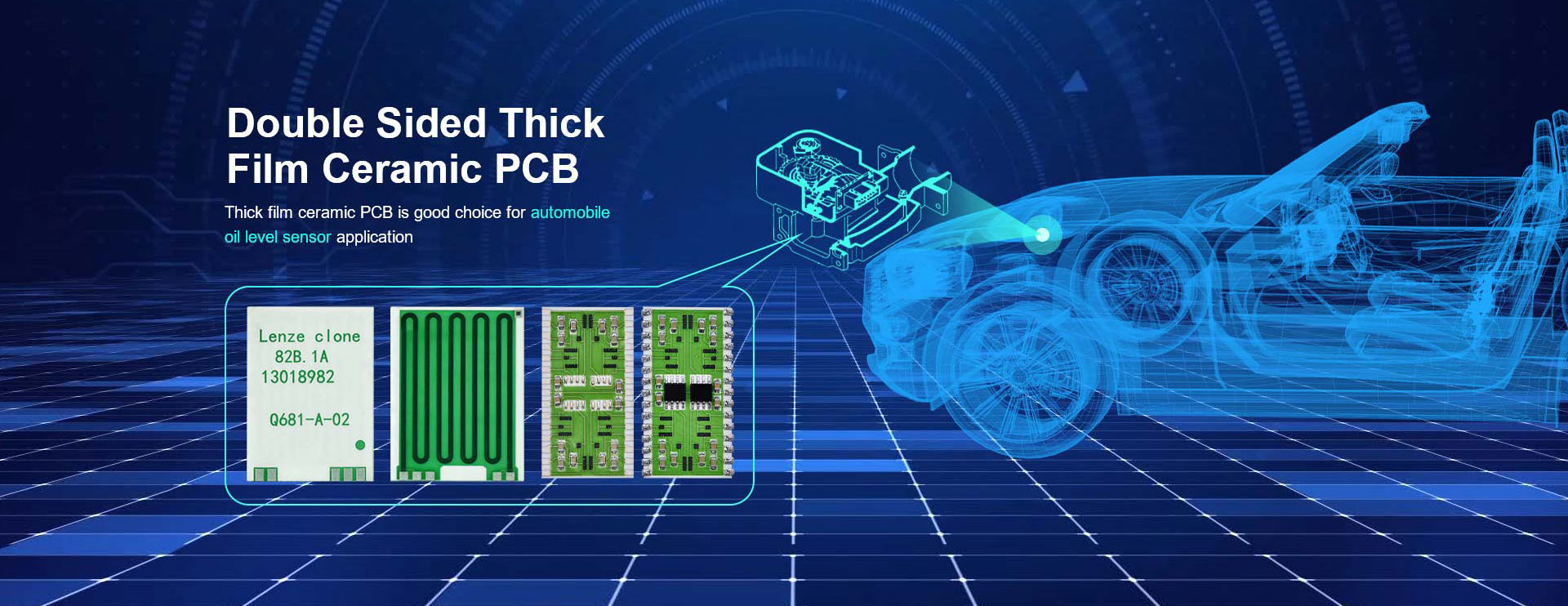
Automotive electronics: With the continuous improvement of automotive electronics, ceramic PCBs meet the high performance and high reliability requirements of automotive electronic equipment with their excellent electrical properties and high temperature resistance.
Telecommunications: In the telecommunications field, the excellent electrical properties and signal integrity of ceramic PCBs ensure the stable operation of high-frequency communication systems, and are an important support for the development of modern communication technology.
LED lighting, semiconductor coolers, high-power semiconductor modules, power control circuits, electronic heaters, intelligent power devices, power hybrid circuits, high-frequency switching power supplies, solid-state relays: In these fields, ceramic PCBs provide guarantees for the stable operation of equipment with their high thermal conductivity, chemical resistance and reliability.
ceramic pcb manufacturer
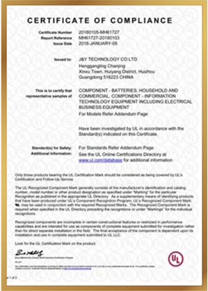
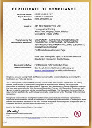
With years of experience in Ceramic PCB R&D, design, and manufacturing, BEST Ceramic Substrates Board is the top three ceramic substrate source factories in Shenzhen, China. Obtained ISO9001, IATF16494, UL, RoHS certification, a one-stop service provider from material procurement, design guidance to production.
Is FR4 ceramic?
Is FR4 ceramic? FR4 is not ceramic. FR4 is a glass fiber reinforced plastic, which is a commonly used electronic industry material, mainly used to make printed circuit boards (PCBs). FR4 material has good electrical insulation and mechanical properties, low cost, and is therefore widely used in situations where electronic connections are required. Ceramics are an inorganic non-metallic material, usually based on aluminum oxide, aluminum nitride or beryllium oxide, with extremely high thermal conductivity and dielectric properties, and are usually used in high temperature, high frequency and high power circuit applications, such as LED lights, power amplifiers, semiconductor lasers, etc.
ceramic pcb vs fr4
FR4 circuit boards are widely used in the manufacture of electronic devices, including but not limited to LED lights, power modules, electric vehicle motor drivers, etc. It is a low-cost and widely used printed circuit board material. Ceramic substrates are mostly used in high thermal conductivity fields due to their excellent physical and chemical properties, such as chip testing and production of IC substrates.
- Material: Ceramic circuit boards are usually made of high-purity ceramic materials, such as alumina, aluminum nitride, etc. FR-4 circuit boards are made of glass fiber cloth and epoxy resin.
- Thermal conductivity: Ceramic circuit boards have high thermal conductivity and can effectively conduct and dissipate heat. FR-4 circuit boards have poor thermal conductivity and weak heat conduction effect.
- Temperature stability: Ceramic circuit boards have good stability in high temperature environments and can withstand high operating temperatures. FR-4 circuit boards have poor temperature stability and are not suitable for working in high temperature environments.
- Flame retardancy: Ceramic circuit boards have good flame retardant properties and can effectively prevent the spread of fire. FR-4 circuit boards have average flame retardant properties and require additional flame retardant treatment.

