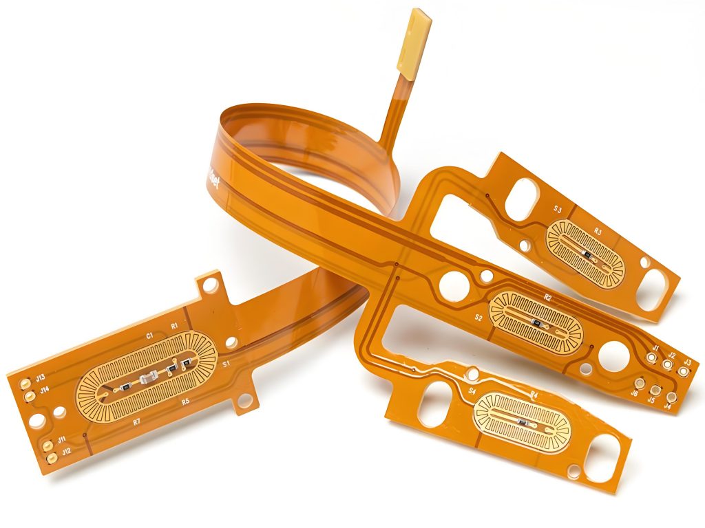
PCB design and fabrication are key steps in producing functional circuit boards for various applications. From simple gadgets to advanced industrial systems, well-designed PCBs ensure performance and reliability. But how does the process work? What factors should designers and manufacturers consider? Let’s dive into the details and uncover the essentials of PCB design and fabrication.
What is the basic rule of PCB design?
Designing a PCB requires precision and adherence to industry best practices. The fundamental rules include:
- Component Placement: Place components logically to ensure minimal signal interference and easy routing. Keep high-speed signals short and direct to reduce noise and improve signal integrity. Group related components together to form functional modules for better organization and easier troubleshooting.
- Trace Routing: Avoid sharp 90-degree angles to minimize signal reflection and interference; use smooth curves or 45-degree angles instead. Keep trace lengths as short as possible, especially for high-speed signals, to reduce signal degradation. Maintain consistent trace widths to ensure even current distribution and minimize impedance variations.
- Power and Ground Planes: Maintain a solid ground plane to improve signal integrity and reduce electromagnetic interference (EMI). Use power planes to provide a stable voltage supply and reduce power distribution impedance. Ensure proper decoupling of power supplies to minimize noise and improve circuit performance.
- Thermal Management: Distribute heat-sensitive components wisely to avoid overheating. Incorporate thermal vias and heat sinks as needed to improve heat dissipation.
- Spacing and Clearance: Ensure proper spacing between traces to avoid short circuits and maintain electrical performance. Adhere to manufacturer-recommended clearances for components and traces to ensure manufacturability.
- Layer Stackup: Choose an appropriate stack-up structure based on the board’s complexity and signal requirements. Properly arrange power planes, ground planes, and signal layers to minimize cross-talk and improve signal integrity.
- Impedance Matching: For high-speed signals, ensure transmission lines match the load impedance to reduce signal reflection and loss. Use controlled impedance traces and terminations as needed to maintain signal integrity.
- Manufacturability and Testability: Design with ease of manufacturing and testing in mind, such as incorporating test points and following the fabricator’s process requirements. Use standard component packages and footprints to ensure compatibility with automated assembly equipment.
In summary, following these basic rules can help designers create PCBs that are functionally optimized, reliable, and manufacturable. At the same time, designers should also flexibly adjust and optimize their design strategies based on specific application requirements and manufacturing process requirements.
Which tool is used to design PCB?
Several PCB design software tools are available, each offering unique features tailored to different needs. Some of the most widely used tools include:
- Altium Designer – Offers an extensive feature set for complex PCB designs and simulation.
- Eagle – A popular choice among both beginners and professionals for its intuitive interface.
- KiCad – An open-source software that provides flexibility and customization.
- OrCAD – Suitable for high-speed and multilayer PCB designs.
- Pads PCB – A professional tool ideal for production-oriented PCB layouts.
Choosing the right tool depends on factors such as project complexity, budget, and ease of use.
How do you draw a PCB design?
Creating a PCB design involves multiple stages, each requiring attention to detail:
- Schematic Capture: The first step is drawing the schematic diagram, defining electrical connections between components.
- Component Selection: Choosing appropriate components based on electrical and thermal requirements.
- PCB Layout: Placing components in a way that minimizes signal interference and optimizes performance.
- Routing Traces: Connecting components using copper traces while following design rules to maintain proper spacing.
- Layer Stackup Design: Defining the number of layers required for signal, power, and ground planes.
- DRC (Design Rule Check): Running automated checks to ensure compliance with spacing, trace width, and clearance guidelines.
- Gerber File Generation: Preparing files for manufacturing, including drill files, solder mask layers, and assembly instructions.
Following these steps helps achieve a design that is manufacturable and meets performance expectations.
What is the difference between PCB layout and design?
PCB design is the entire process, from conceptualizing the circuit to generating manufacturing files. PCB layout, on the other hand, is a specific step within the design process that focuses on placing components and routing traces. Simply put, design includes planning and simulation, while layout is more about the physical arrangement of components and interconnections.
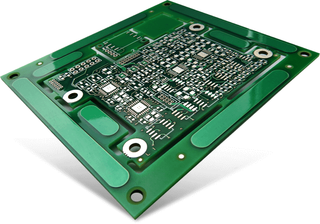
What is PCB design process?
What is PCB design process? The PCB design process follows a structured approach:
- Concept and Requirements: Define the application, specifications, and constraints.
- Schematic Design: Draw the circuit diagram, specifying how components connect.
- PCB Layout Design: Place components and route traces while considering signal integrity and thermal management.
- Simulation and Testing: Validate the design using software simulations to detect potential issues.
- Prototype Fabrication: Manufacture a prototype PCB for testing.
- Design Iteration: Make necessary modifications based on testing results.
- Final Design Approval: Ensure all aspects meet industry standards before mass production.
A well-planned design process minimizes errors and improves efficiency.
What is the difference between PCB fabrication and manufacturing?
PCB fabrication refers to the process of creating the bare board, which includes etching copper layers, drilling holes, and applying solder masks. PCB manufacturing is a broader term that encompasses fabrication as well as component assembly, soldering, and final testing. In simple terms, fabrication makes the board, while manufacturing completes the final product with all components attached.
What is the difference between PCB fabrication and assembly?
PCB fabrication is the process of building the physical board, while PCB assembly involves placing and soldering components onto the board. Fabrication deals with raw materials and structure, whereas assembly turns the fabricated board into a fully functional circuit.
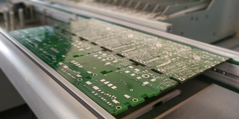
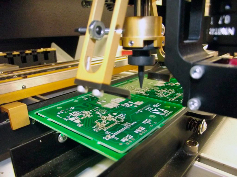
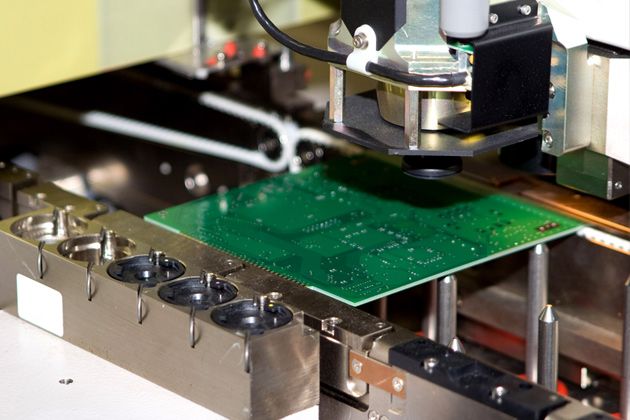
What is the fabrication process in PCB?
The PCB fabrication process consists of multiple steps:
- Design Transfer: Convert PCB design files into a format suitable for manufacturing.
- Substrate Preparation: Choose materials like FR4, ceramic, or metal-core for the PCB.
- Layer Stacking: Arrange multiple layers for multilayer PCB designs.
- Drilling: Create holes for vias and component leads using high-precision drilling machines.
- Copper Deposition: Apply copper layers through electroplating or other techniques.
- Etching: Remove excess copper to form conductive traces.
- Solder Mask Application: Apply a protective layer to prevent oxidation and short circuits.
- Silkscreen Printing: Add component labels and markings for easy identification.
- Surface Finish Application: Enhance solderability with finishes like HASL, ENIG, or OSP.
- Final Inspection: Perform electrical testing and visual inspections to ensure quality.
Each step plays a crucial role in producing a high-performance PCB.
PCB Design and Fabrication Manufacturer
Why choose Best Technology as your PCB design and fabrication manufacturer? Choosing the right partner for PCB design and fabrication is essential for achieving high-quality, reliable, and cost-effective circuit boards. At Best Technology, we take pride in delivering top-tier PCB solutions backed by 18 years of expertise, advanced manufacturing capabilities, and customer-centric service. Here’s why we stand out as the ideal choice for your PCB needs.
1. Over 18 Years of PCB Manufacturing Excellence
With nearly two decades in the PCB industry, we understand the intricacies of pcb design and fabrication. Our skilled engineers specialize in layout optimization, signal integrity management, and material selection to enhance PCB performance and durability. Our vast experience allows us to handle everything from designing to large-scale fabrication effortlessly.
2. No Minimum Order Quantity (MOQ)
We cater to all project sizes, whether you need a single prototype for testing or bulk fabrication for mass production. Our flexible approach enables startups and enterprises alike to scale production without compromising quality or efficiency.
3. Fast Turnaround with Reliable Delivery
We recognize the importance of quick time-to-market. Our streamlined production processes ensure PCB delivery within 2-3 weeks, and we offer expedited fabrication options for urgent projects. Our efficient logistics and supply chain management guarantee on-time delivery every time.
3. Cutting-Edge Manufacturing Technology
Best Technology invests in state-of-the-art production facilities and advanced engineering techniques to manufacture high-precision PCBs. Our capabilities include:
- High-Density Interconnect (HDI) technology for compact and complex designs.
- Laser drilling and fine-line etching for superior accuracy.
- Automated Optical Inspection (AOI) and X-ray inspection for defect detection.
- Selective wave soldering and precision reflow soldering for robust assemblies.
4. Strict Quality Control and Testing Standards
Quality and reliability are at the core of our PCB fabrication process. We implement rigorous testing procedures to ensure defect-free and high-performance circuit boards. Our quality control measures include:
- Electrical Testing (E-Test) to verify circuit continuity.
- Impedance Control Analysis for high-frequency applications.
- Thermal Stress Testing to evaluate durability under extreme conditions.
- Automated and Manual Inspections to maintain consistency and accuracy.
5. Certified PCB Fabrication Facilities
We adhere to global industry standards, ensuring that our PCBs meet the highest levels of quality and compliance. Our certifications include:
- ISO 9001 – Quality Management System
- ISO 13485 – Medical Device Manufacturing Standard
- IATF 16949 – Automotive Industry Standard
- AS9100D – Aerospace Industry Certification
- RoHS & REACH Compliance – Environmentally Friendly Manufacturing
6. Expert Technical Support and Engineering Consultation
At Best Technology, customer satisfaction is our priority. Our experienced engineers provide end-to-end support, from design consultation and material selection to performance optimization and troubleshooting. If you need assistance with complex PCB design and fabrication, our technical team is available 24/7 to help you achieve the best results.
Best Technology is committed to delivering high-quality PCB design and fabrication services that meet the evolving needs of modern electronics. Our experience, advanced capabilities, and customer-focused approach make us the trusted choice for businesses seeking superior PCB solutions. Whether you’re developing a new product or improving an existing design, we are here to provide expert guidance and manufacturing excellence every step of the way.
In conclusion, understanding PCB design and fabrication is essential for creating durable and efficient circuit boards. By following best practices, using the right tools, and ensuring proper fabrication processes, high-quality PCBs can be produced. If you’re looking for a trusted partner in PCB design, fabrication, and assembly, Best Technology offers over 18 years of expertise in delivering top-notch PCBs. Feel free to contact us at sales@bestpcbs.com for any doubts or queries you might have.