
PCB Via Current Calculator
| PCB Vias current flow calculator | ||
|---|---|---|
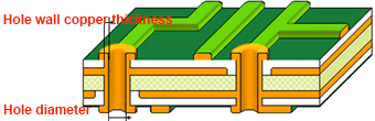
| Hole diameter: | ||
| Hole wall copper thickness: | ||
| Temperature rise: | ||
| Current: | Amps | |
 |
||
| Note: Follow IPC-2221 standard, calculator results are only for reference.
|
||
PCB Via Current Calculator
When laying out, not only the wire's ability to withstand large currents and voltage drop losses should be considered.
Similarly, the size of the via should also be considered for its ability to withstand currents.
If the via diameter is too small and the current is large, it is easy to cause the copper foil on the hole wall to burn out.
Possible phenomena:
The initial performance of the product is good, but after a period of use, a fault suddenly occurs and is difficult to find.
How to Calculate Current Carrying Capacity in PCB Via
The calculation of the overcurrent capacity of PCB (printed circuit board) vias is usually based on the following key parameters:
Via diameter (D): The diameter of the via determines its effective conductive cross-sectional area, which in turn affects the current carrying capacity.
Copper thickness (t): The thickness of the inner or outer copper foil has a direct impact on the resistance of the via.
Material resistivity (ρ): The resistivity of copper is about 1.72×10^-8 Ω·m at room temperature.
Via length (L): That is, the thickness of the PCB board, which is an important factor in the calculation of via resistance.
Allowable temperature rise (ΔT): According to application requirements and material properties, a maximum allowable temperature rise is specified to ensure the safe operation of components.
Heat dissipation conditions: including the thermal conductivity of the PCB material, the ambient temperature, and whether there are heat dissipation measures.
The resistance of the via can be estimated by the following formula:
Math
1R_via = ρ * L / (π * (D/2)^2)
Then, the heat generated by the via is calculated using Joule's law:
Math
1P = I^2 * R_via
Where P is the power loss and I is the current through the via.
In order to ensure that the via is not damaged due to excessive heat, its temperature rise needs to be limited. Therefore, combined with the heat dissipation conditions, a maximum allowable power loss can be set. Through this limit value, the maximum continuous operating current that the via can withstand is inferred.
Example to Illustrate Via Size Calculation Method
Example: A PCB design project requires that the temperature rise does not exceed 20℃, the via wall copper thickness is 1OZ (1.38mil), and the via current carrying capacity is 1A. Calculate the via inner diameter size.
- 1) Check the IPC-2152 Conservative Chart (Figure D). It can be seen that when the temperature rise is 20℃ and the current carrying capacity is 1A, the cross-sectional area corresponding to the intersection is about 28mil2. According to formula 5, the equation can be obtained: π (D.D - d.d)/4=28mil2.
- 2) Knowing that the via wall copper thickness is 1OZ (1.38mil), the equation can be obtained: D-d=1.38mil.
- 3) According to the equation and the equation, we can get: d=7.28mil (0.185mm).
Answer: When the temperature rise is 20℃, the current is 1A, and the copper thickness is 1OZ, the inner diameter of the via is set to 0.185mm to meet the requirements, and the margin is large, which is very safe to use.
Note: The relationship between the thickness of the outer copper skin and the thickness of the electroplated layer on the via hole wall: Assuming that the surface finished copper thickness is required to be 1OZ, when producing PCB, first paste about 1/3OZ of copper skin on the surface, then drill holes, and then use chemical methods to deposit nickel on the hole wall for about 1/3OZ. Finally, when electroplating, electroplate 2/3OZ of copper on the surface and the hole wall, so that the total thickness of the surface copper skin and the via nickel copper is equal, but in actual production, the total thickness of the via nickel copper (also called electroplating layer) is equal to or slightly less than the total thickness of the surface copper foil.