LED Ring PCB is very important to many modern lighting applications. Because these specialized printed circuit boards allow LEDs to be arranged in a circular configuration, offering uniform lighting with efficient power use. In this blog, we’ll explore together everything you need to know about LED ring PCBs, from their design and materials to the advantages they offer and the best manufacturers to work with.
What Is LED Ring PCB?
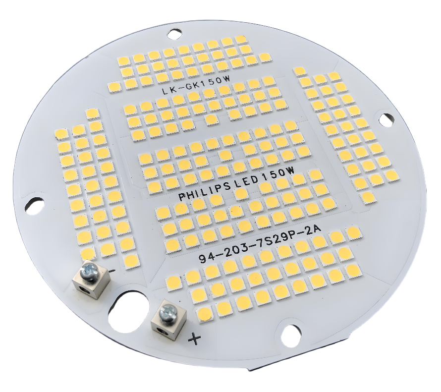
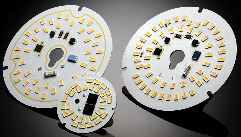
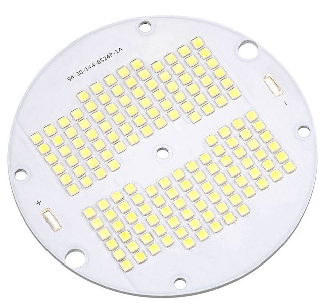
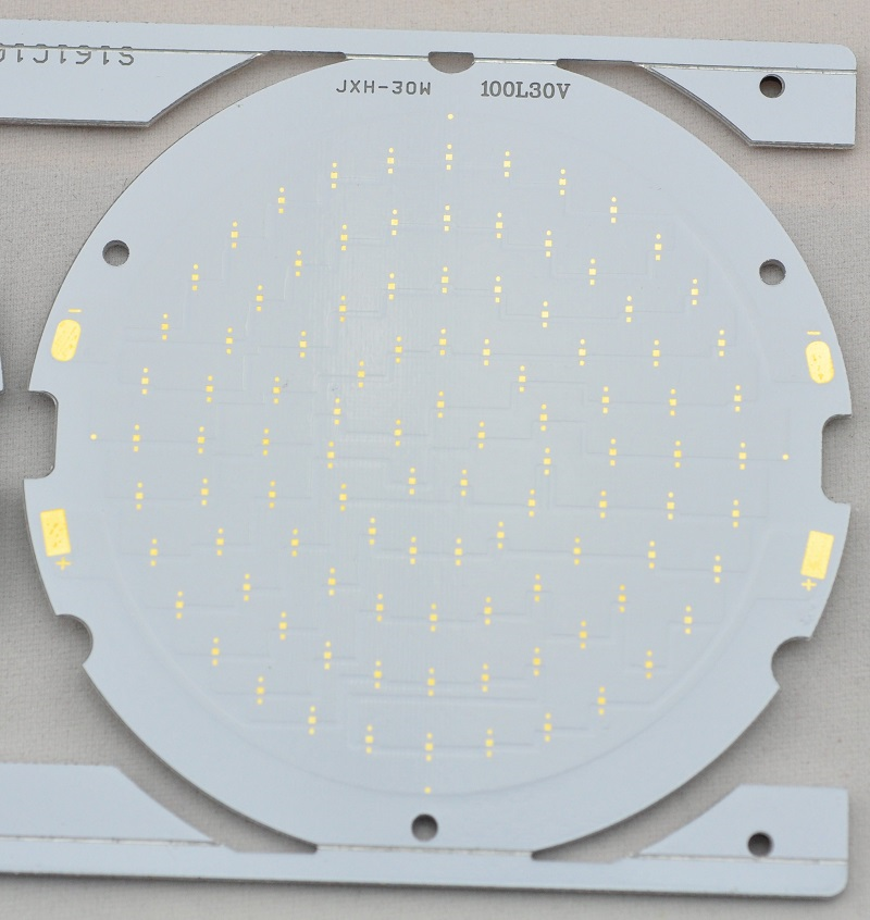
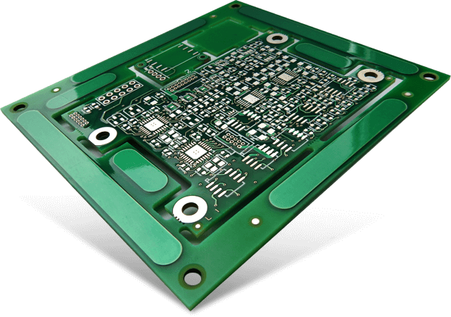
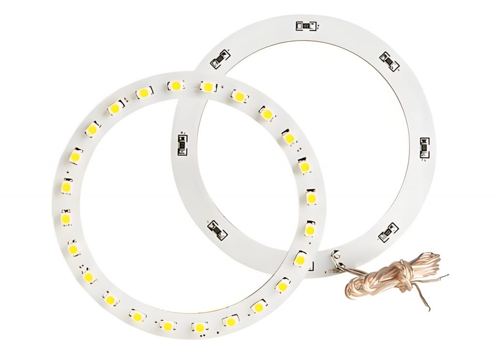
A LED ring PCB is a circular printed circuit board that houses multiple LEDs. These boards are engineered to efficiently manage the distribution of electrical current to each LED, ensuring consistent lighting. The design of the PCB allows LEDs to be placed in a circular pattern, optimizing light output and creating a uniform glow. Whether you’re designing a lighting solution for commercial use, automotive applications, or decorative purposes, LED ring PCBs boards are versatile and customizable, making them a popular choice for a wide range of industries.
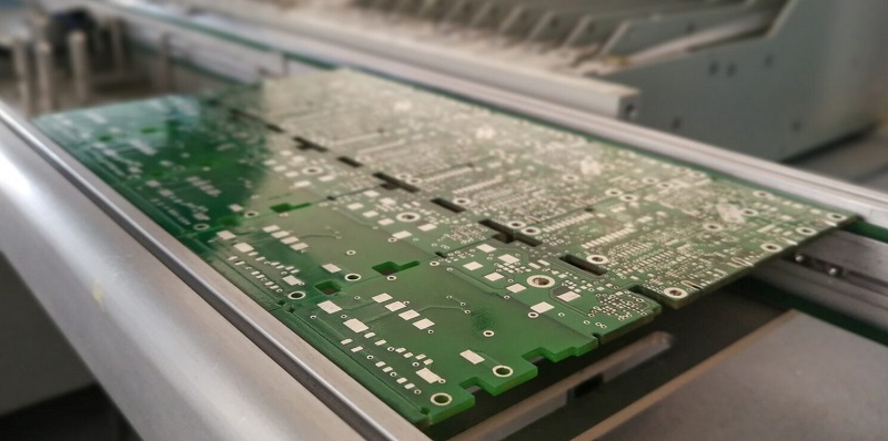
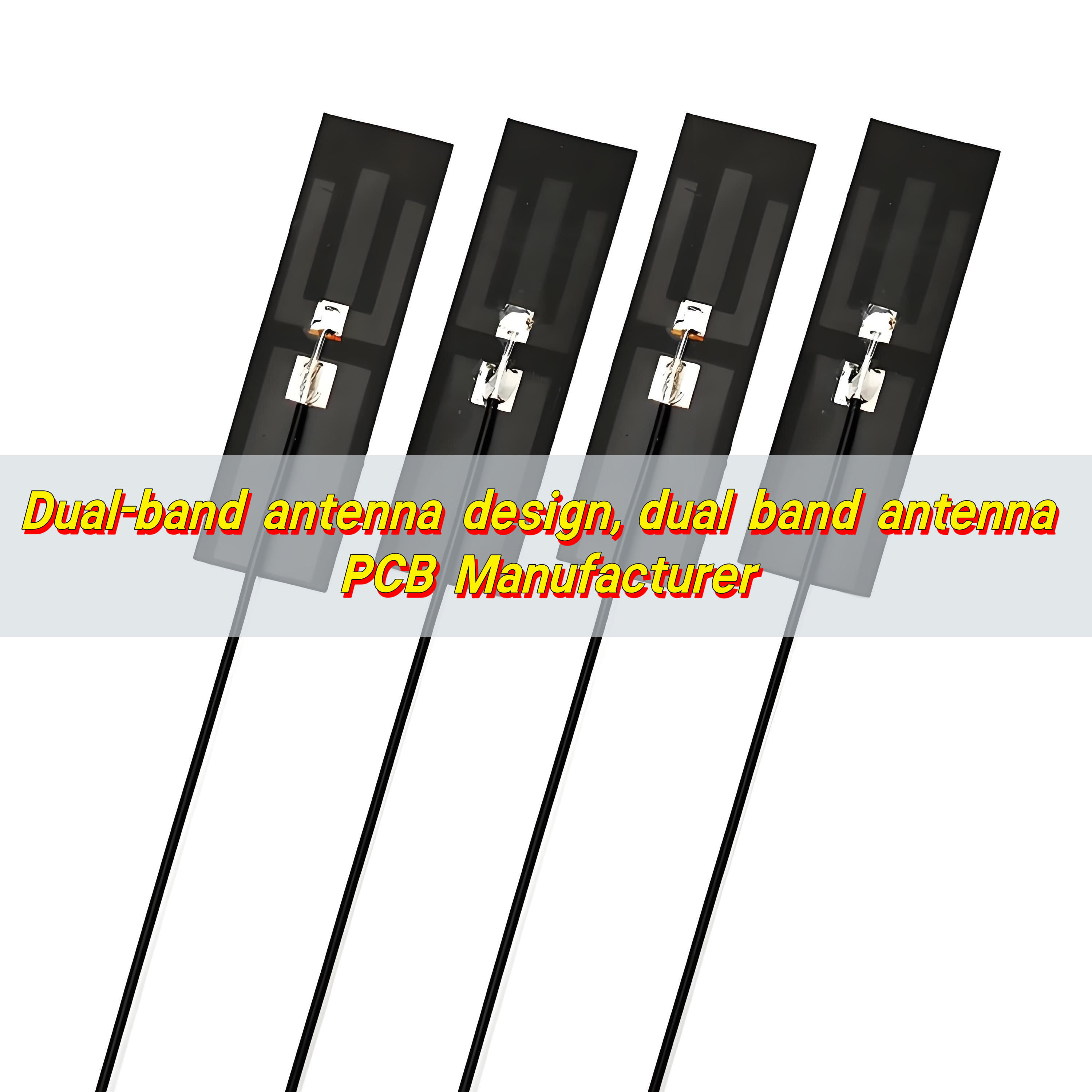
Best technology specialize in high quality LED ring PCB design, prototype and manufacturing and PCBA services over 18 years. In order to strictly control every step of production from raw material procurement to finished product delivery, we have established a strict quality system and worked hard to obtain ISO certification. And we adopted automatic optical inspection (AOI) and X-ray, it ensures that each printed circuit board (PCB) meets or even exceeds industry standards. Then we have our own LED PCB manufacturing industry chain and experienced production teams, So we are able to provide you with high quality LED PCB products and fast delivery. Welcome to contact us at sales@bestpcbs.com if you’re interested in us.
Advantages of LED Ring PCB
Here are some of the most significant advantages of LED Ring PCB Board:
- Uniform Light Distribution: It ensures that the emitted light is even, without bright spots or shadows. It’s ideal for applications like decorative lighting or photography where consistent lighting is crucial.
- Energy Efficiency: LEDs are known for their energy-saving capabilities, and when placed on a ring PCB, they offer even greater energy efficiency. LED ring PCBs provide high brightness while consuming less power, making them cost-effective in the long run.
- Compact and Flexible Design: LED ring PCBs come in compact sizes that allow them to fit into tight spaces, such as around cameras, mirrors, or small appliances. Flexible variants allow you to bend and shape the board to suit your needs, which is ideal for automotive or wearable devices.
- Durability and Longevity: LED ring PCBs are made from high-quality materials that are resistant to wear and tear. Many manufacturers use aluminum or copper substrates, which offer better heat dissipation and contribute to the longevity of the LEDs.
- Versatility in Applications: From decorative lighting to automotive headlights, LED ring PCBs can be used in many different settings. Their adaptability and efficiency make them an excellent choice for a variety of lighting applications.
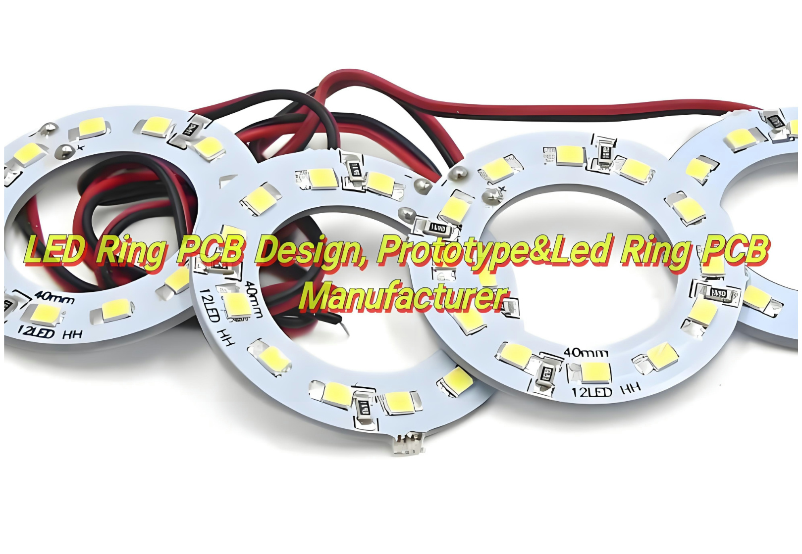
Advantages of LED Ring PCB
Application of LED Ring PCB
LED ring PCBs have a wide range of applications. Here are some of the most popular uses:
- Decorative and Ambient Lighting: Used in interior lighting. Their ability to emit a soft, even light makes them ideal for home decor, accent lighting, and signage. You’ll find them in everything from lighted mirrors to wall sconces.
- Automotive Lighting: Used in headlamps, taillights, and interior lighting. The circular shape allows for efficient distribution of light, enhancing visibility while also providing a modern aesthetic.
- Photography and Videography: Use LED ring PCBs to create soft, flattering light for their subjects. These ring lights provide even lighting, minimizing shadows and giving photos a polished look. They’re also popular in video production for creating clean, bright lighting around the camera.
- Wearables and Devices: Used in wearable technology. For example, they may be incorporated into smartwatches or fitness trackers, where the compact design can be integrated without sacrificing performance.
- Signage and Advertising: LED ring PCB are used in outdoor signage and advertising displays. Their ability to produce bright, consistent light ensures that these signs are visible even in low-light environments.
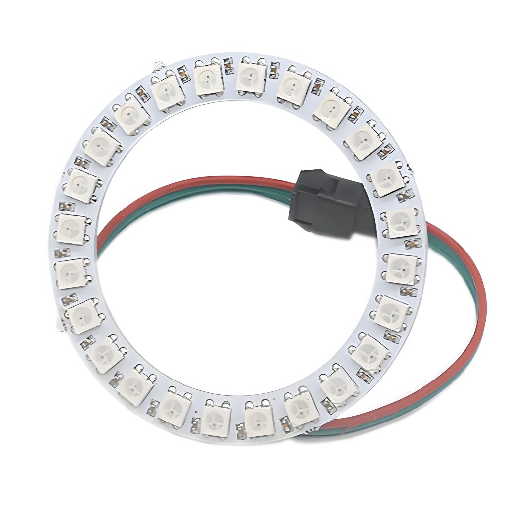
Application of LED Ring PCB
Types of LED Ring Light PCB
The classification of LED Ring Light PCB can be detailed from three aspects: materials, number of layers, and structure.
Material Classification
Organic Materials:
- Phenolic resin: it has the characteristics of weak acid and weak alkali resistance, but not strong acid and strong alkali resistance, insoluble in water but soluble in organic solvents such as acetone and alcohol.
- Glass fiber: an inorganic non-metallic material with good insulation, heat resistance, corrosion resistance and high mechanical strength, but brittle and poor wear resistance.
- Polyimide (PI): a high-performance polymer with a variety of forms and molding methods, widely used in aerospace and biomedical fields.
- Epoxy resin and BT: also organic materials with specific application scenarios.
Inorganic Materials:
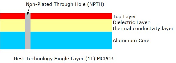
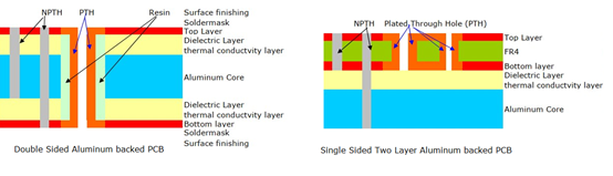
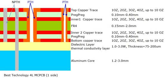
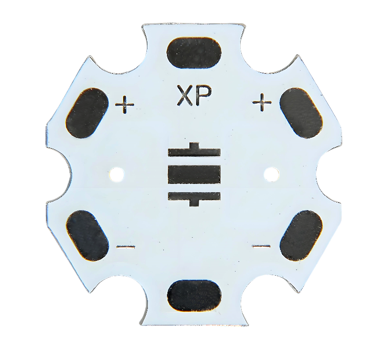
- Aluminum substrate: a metal-based copper-clad laminate with good heat dissipation function, commonly used in LED lighting products, usually composed of a circuit layer (copper foil), an insulating layer and a metal base layer.
- Copper substrate: better thermal conductivity than aluminum substrate and iron substrate , suitable for high-frequency circuits and environments with large changes in high and low temperatures.
- Ceramic substrate: Using its heat dissipation function, it is suitable for specific application scenarios.
Number of Layers Classification
- Single-sided board: Parts are concentrated on one side, and wires are on the other side, suitable for simple circuit requirements.
- Double-sided board: A printed circuit board with conductive patterns printed on both sides, and the conductive patterns on both sides are connected by metallized holes, suitable for more complex circuit requirements.
- Multilayer board: It has three or more layers of conductive patterns, the inner layer is made of conductive patterns and insulating semi-cured sheets laminated and pressed, and the outer layer is copper foil, suitable for circuit design with high density and high performance requirements.
Structural Classification
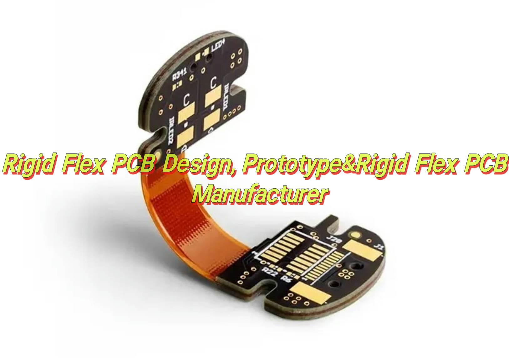
- Rigid board: It has excellent bending resistance and support, suitable for circuit design that requires stable support.
- Flexible board: It can be bent and folded, suitable for application scenarios with limited space.
LED PCB Manufacturers
Choosing the right LED ring PCB manufacturer is crucial to ensuring that you receive high-quality products that meet your design specifications. Best Technology, with over 18 years of experience in the industry, is a leading manufacturer of LED ring PCBs. Here’s why you should consider partnering with us:
- Customization Options: We offer a range of customizable LED ring PCB designs. Whether you need specific sizes, shapes, or materials, our team can work with you to create the perfect solution.
- High-Quality Materials: At Best Technology, we use top-tier materials like aluminum, copper, and polyimide to ensure the durability and performance of our LED ring PCBs. Our products are designed to withstand wear and provide long-lasting performance.
- Competitive Pricing: We offer competitive prices without compromising on quality. Our goal is to provide cost-effective solutions that help bring your designs to life.
- Global Reach: With a broad customer base and international shipping, Best Technology is equipped to handle projects of any size, whether you’re based locally or internationally.
What Materials Are Used in LED PCB?
The materials used in LED ring PCBs play a significant role in their performance and durability. Here are some of the most common materials:
- FR4: This is the most commonly used material for LED ring PCBs. It’s a durable and cost-effective substrate that works well for general applications.
- Aluminum: For high-power applications, aluminum is used as a substrate material. It has excellent heat dissipation properties, making it ideal for high-performance LED ring PCBs.
- Copper: Copper is often used for high-conductivity applications. It helps to enhance the performance of LED ring PCBs by improving heat transfer and reducing electrical resistance.
- Polyimide(PI): For flexible designs, polyimide is a popular choice. It’s durable, flexible, and resistant to high temperatures, making it suitable for bending and shaping applications.
How To Design LED Ring PCB?
The process of LED ring PCB design involves several steps:
1. Define Your Requirements and Specifications
The first step in any PCB design is to define your needs and specifications. For LED ring PCBs, this includes determining several key factors:
- Size and Shape: The size of the LED ring PCB will be dictated by the physical space available in your project. Are you creating a large display, a compact wearable device, or a decorative lighting solution? This will determine the diameter of your PCB and the number of LEDs to be used.
- LED Configuration: Decide on how many LEDs you want to arrange in the circle. The number of LEDs will influence the brightness and uniformity of the light emitted by the ring. Be sure to space the LEDs evenly for consistent light distribution.
- Power Requirements: LEDs require a specific amount of voltage and current. Determine the power requirements of the LEDs you plan to use. Ensure the PCB is capable of supplying the necessary power to each LED without overheating or causing circuit instability.
- Type of LED: LED ring PCBs can house different types of LEDs, such as standard SMD (Surface-Mount Device) LEDs, high-power LEDs, or flexible LEDs. Your choice of LED type will affect the overall design of the PCB.
- Voltage and Current Considerations: Ensure the voltage and current ratings match the specifications for both your LED ring and the power supply. Consider using a constant current driver to regulate the current supplied to the LEDs, preventing power fluctuations.
2. Select the Right Materials for Your PCB
The materials you choose for your LED ring PCB will significantly affect the performance of the final product. Here are the most commonly used materials:
- FR4 (Glass-Fiber Epoxy): This is the most common material used in PCB manufacturing. It’s affordable, durable, and suitable for general lighting applications. FR4 is ideal for low to medium power LEDs.
- Aluminum (Metal Core PCB): For high-power LEDs, aluminum is often used as the base material for the PCB. Aluminum offers superior heat dissipation, preventing the LEDs from overheating and ensuring they operate at peak efficiency. Aluminum-based LED PCBs are commonly used in industrial or automotive applications.
- Copper: Copper is another material used in LED ring PCBs for its excellent thermal conductivity. Copper-based designs help to quickly dissipate heat generated by high-power LEDs, keeping the system stable and extending its lifespan.
- Polyimide: For flexible LED ring PCBs, polyimide is a preferred material. It is flexible, durable, and resistant to high temperatures, which makes it ideal for applications that require bending or shaping, such as wearable devices or automotive lighting.
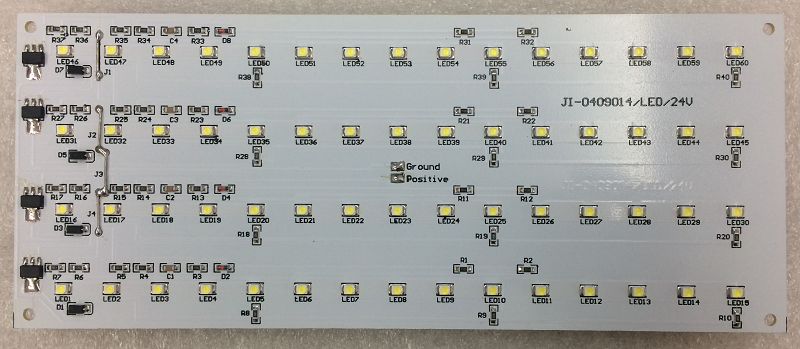
3. Create the Circuit Design and Layout
Once you’ve defined your specifications and chosen the materials, it’s time to create the circuit layout. This is where the technical aspects of your LED ring PCB come into play:
LED Placement: The most important aspect of your design is the placement of the LEDs in a circular configuration. Ensure that the LEDs are evenly spaced to ensure uniform light output. If you’re using high-density LEDs, make sure to account for the necessary spacing to prevent heat buildup.
- Power Distribution: Plan the power distribution for your LED ring. You must ensure that each LED gets the correct amount of power. For larger designs, consider creating multiple power supply points around the ring to avoid voltage drops and ensure each LED is supplied with stable power.
- Current Control: In most LED applications, a constant current driver is used to regulate the current flowing through the LEDs. This helps maintain consistent brightness and prevents damage to the LEDs. Design the circuit to include appropriate resistors or constant current drivers to manage power flow effectively.
- Heat Dissipation: LEDs generate heat, so effective heat management is a crucial part of the design. Ensure that your PCB layout includes a clear path for heat dissipation. If you’re using metal-core PCBs, the aluminum or copper material will help carry away heat, but proper trace widths and vias are essential to enhance the thermal conductivity.
- Trace Widths and Via Sizes: Calculating the correct trace width and via size is critical for ensuring that the PCB can handle the required current without overheating. Use PCB design software that can help you calculate trace widths based on the current requirements for your LEDs.
4. Consider Power Supply and Drivers
The power supply is a key consideration in LED PCB design. LED rings require a regulated power supply to provide a consistent voltage and current to the LEDs. Here’s what you need to think about:
- Power Supply Type: Depending on the voltage and current requirements of your LED ring, you’ll need to select an appropriate power supply. A common solution is using a constant current driver, which adjusts the current flowing to the LEDs to ensure that they don’t receive too much power, which could lead to burnout.
- Voltage Regulation: Ensure that the power supply can deliver a constant voltage that matches the voltage requirement of your LEDs. Many LEDs operate on low voltage, and using a higher voltage power supply without regulation could cause instability.
- Efficiency Considerations: LED drivers and power supplies should be as efficient as possible to minimize energy loss. Look for energy-efficient drivers that can help you reduce power consumption, which is especially important in battery-powered or low-power applications.
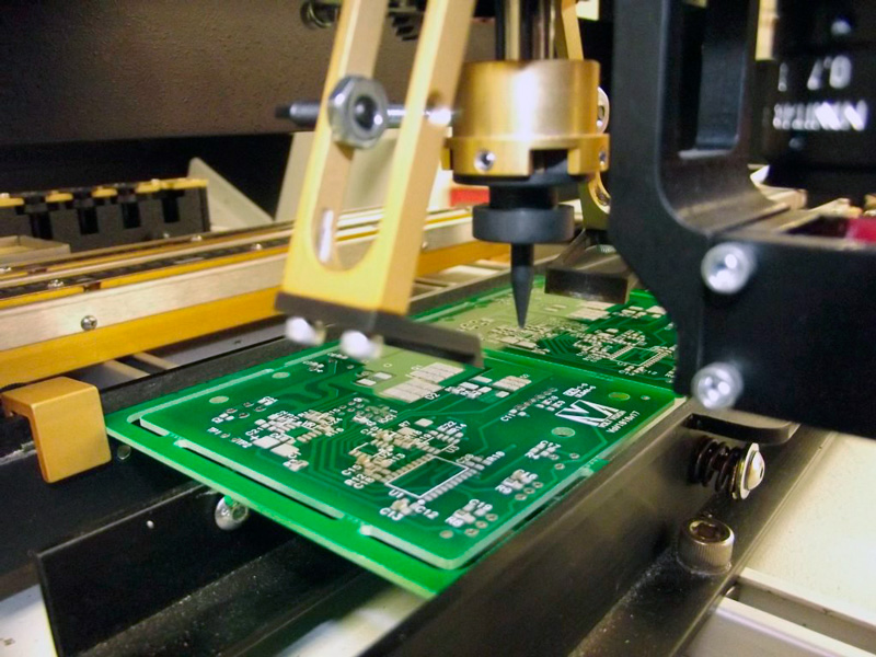
5. Prototype and Test Your LED Ring PCB
Once your design is complete, the next step is to prototype your LED ring PCB. This stage involves manufacturing a small batch or a single unit of your design for testing. LED Ring PCB Prototyping is essential for checking the functionality of the circuit, ensuring the LED ring lights up correctly, and verifying that the power distribution is stable.
Here’s how to proceed:
- Manufacturing the Prototype: After designing the PCB, the next step is to send the design files to a PCB manufacturer for production. The manufacturer will produce the prototype based on the materials, size, and specifications you’ve provided.
- Testing the Prototype: Once you receive your prototype, it’s time to test it. Check that all LEDs light up as expected, and that there are no issues with flickering or uneven light. Verify that the power distribution works well and that the PCB doesn’t overheat.
- Thermal Testing: For high-power designs, thermal testing is crucial. Monitor the temperature of the LEDs during operation to ensure that the heat dissipation is working correctly. If the PCB gets too hot, you may need to make adjustments to the trace widths, vias, or use a more efficient heat sink material.
- Adjustments and Iterations: Based on the results of your testing, you may need to make design adjustments. This might involve tweaking the power distribution, changing materials, or adjusting the size of certain components.
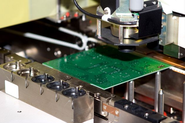
6. Move to Mass Production
Once the prototype has been successfully tested and approved, you can move on to mass production. Working with a reliable LED PCB manufacturer is key at this stage to ensure that the final product meets all of your quality and design specifications.
If you’re looking for a trusted LED PCB manufacturer, Best Technology offers exceptional LED PCB solutions, with extensive experience in designing, prototyping, and mass producing LED ring PCBs.
Conclusion
To sum up, LED ring PCB are essential components for creating efficient, durable, and high-quality lighting systems. Whether you’re designing for decorative lighting, automotive applications, or commercial displays, understanding the key aspects of LED ring PCBs is critical. Best Technology’s expertise in manufacturing LED PCBs ensures that you get top-notch products tailored to your needs. With the right design, materials, and manufacturer, you can create lighting solutions that are both visually appealing and performance-driven.